HAL Id: hal-01922765
https://hal.archives-ouvertes.fr/hal-01922765
Submitted on 14 Nov 2018
HAL is a multi-disciplinary open access
archive for the deposit and dissemination of
sci-entific research documents, whether they are
pub-lished or not. The documents may come from
teaching and research institutions in France or
abroad, or from public or private research centers.
L’archive ouverte pluridisciplinaire HAL, est
destinée au dépôt et à la diffusion de documents
scientifiques de niveau recherche, publiés ou non,
émanant des établissements d’enseignement et de
recherche français ou étrangers, des laboratoires
publics ou privés.
Accurate Channel Models for Realistic Design Space
Exploration of Future Wireless NoCs
Ihsan El Masri, Pierre-Marie Martin, Hemanta Mondal, Rozenn Allanic,
Thierry Le Gouguec, Cédric Quendo, Christian Roland, Jean-Philippe Diguet
To cite this version:
Ihsan El Masri, Pierre-Marie Martin, Hemanta Mondal, Rozenn Allanic, Thierry Le Gouguec, et al..
Accurate Channel Models for Realistic Design Space Exploration of Future Wireless NoCs. 2018
Twelfth IEEE/ACM International Symposium on Networks-on-Chip (NOCS), Oct 2018, Turin, Italy.
�hal-01922765�
Accurate Channel Models for Realistic Design Space
Exploration of Future Wireless NoCs
Special Session Paper Ihsan El Masri Lab-STICC UBO Brest, France [email protected] Pierre-Marie Martin Lab-STICC UBO Brest, France [email protected]
Hemanta Kumar Mondal Lab-STICC UBS Lorient, France [email protected] Rozenn Allanic Lab-STICC UBO Brest, France [email protected] Thierry Le Gouguec Lab-STICC UBO Brest, France [email protected] Cédric Quendo Lab-STICC UBO Brest, France [email protected] Christian Roland Lab-STICC UBS Lorient, France [email protected] Jean-Philippe Diguet Lab-STICC CNRS Lorient, France [email protected]
Abstract— Wireless Networks-on-Chip (WiNoC) are being
explored for parallel applications to improve the performances by reducing the long distance/critical path communications. However, WiNoC still require precise propagation models to go beyond proof of concept and to demonstrate it can be considered as a realistic efficient alternative to wired NoC. In this paper, we present accurate 3D models based on measurements in Ka band and Electromagnetic (EM) simulations of transmission on silicon substrate in the V band and the Sub-THz band. Using these EM results, a time-domain simulation is performed using an On-Off Keying (OOK) modulation based transmission with different PA/LNA configurations. Our results highlight the type of performances and tradeoffs to be considered according to different parameters such as power output and amplifier’s gain. By improving the knowledge about the signal propagation, one can conduct precise design space exploration for parallel applications. We discuss the realistic channel modeling and we present also hybrid solutions and associated limitations of WiNoC architectures. We conclude the paper with research directions to be explored to make WiNoC a reality.
Keywords—Dipole antennas, electromagnetic propagation, network-on-chip, parallel application, wireless channel modeling
I. INTRODUCTION
The emergence of the High-Power Computing (HPC) applications, leads to manycore architectures, which necessitates the use of efficient network-on-chip. However, the future manycore architectures will require large NoC that can lead to prohibitive latencies due to long multi-hop paths. Parallel computing relies on cache coherency protocols and synchronization mechanisms (locks, barriers, conditions). The efficiency of cache coherence protocols and synchronization is strongly penalized by multi-hop paths and by sequential messages. There is a great need of alternative solutions to avoid this penalization in parallel computing.
Wireless Networks-on-Chip (WiNoC) is considered as a promising solution in the context of manycore architectures to replace the multi-hop communications [1]. The use of wireless links allows single-hop long distance communication between distant nodes. WiNoC also allows taking benefit of real
broadcast capabilities. Most existing WiNoC architectures are based on On-Off Keying (OOK) modulation technique as it is power and area efficient. Currently, CMOS-compatible NoC with millimeter-wave (mm-wave) wireless links proves reasonable bandwidth and energy efficiency. With technology advances, mm-wave transceiver can also provide high bandwidth to fulfill the application needs.[2]
However, WiNoC still suffer from important limitations. The first one is the power consumption of the analog part of the transceivers with its order of magnitude (tens of mW) larger than the power consumption of digital components. Apart from the transceiver component in WiNoC, channel modeling is one of the major concerns. The multiple important radio parameters with strong impacts on communication quality and efficiency are not considered or based on simple and non-meaningful models. Accurate models are complex but signal propagation in air or silicon layers must be taken into account with its physical phenomena implications such as multipath interferences, metal interference structures and time-domain dispersion [3]. Thus, there is a need of a detailed investigation on channel modeling and antenna models before proceeding to a complete realization of the wireless links at a network level.
The BBC project (on-chip wireless Broadcast-Based parallel Computing) [4] has as an objective the realization of wireless interconnects for parallel computing application. A complete study is entailed from the radio and physical layer (i.e. the design and study of an integrated antenna /transceiver and of the propagation channel) through the MAC layer to the digital layer (broadcast protocol/architecture).
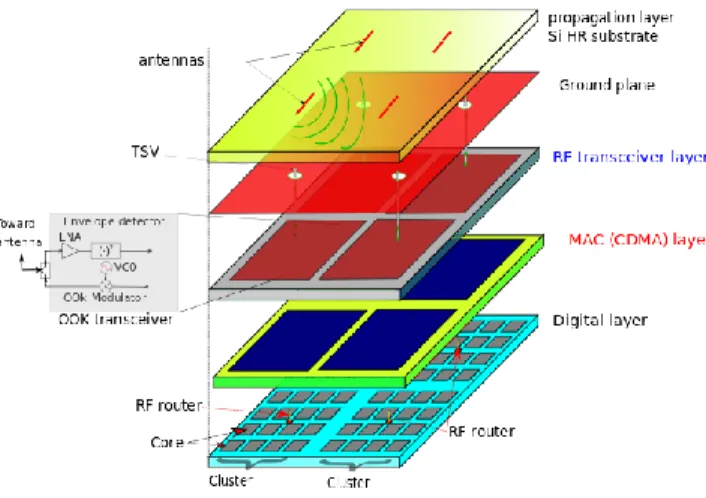
In this article, we present in the context of BBC an accurate model based on measurements and electromagnetic (EM) simulations of transmission on silicon substrate, in order to facilitate the efficient design of on-chip wireless communication infrastructure. After validating the problems caused by the silicon substrate by measurement, we propose a solution and test its feasibility by EM simulation on 2 different simulation tools and deduce its implications and benefits on the overall system. The retained multilayer architecture for BBC project is illustrated in Fig. 1.
Fig. 1 : The different layers of a Wireless network on Chip
The remainder of the paper is organized as follows: a brief overview of existing channel modeling works is presented in Section II. Section III describes the propagation channel measurement and analysis in frequency domain. The time domain analysis of propagation channel is illustrated in Section IV. Overall summary of this work including feasibility, scalability and overheads is discussed in Section V. We conclude our work in Section VI.
II. RELATED WORKS
Emerging interconnect architectures tend to reduce performance limitations of multi-hop communication in conventional wired NoCs. Four emerging interconnects are explored to address the long-range multi-hop communication bottleneck [5]: three-dimensional (3D) [6], photonic [7], RF/wireless NoC [8]. The mm-wave based WiNoCs have emerged as one of the promising solutions for scalable, energy-efficient CMOS compatible technology. Another alternative to wireless interconnects is an inductive/capacitive-coupled 3D integration technology [9], [10], however it produces electromagnetic interferences through the unwanted coupling. Thus, we choose to use mm-wave interconnects as it is the most adequate for broadcast application.
The WiNoC system has two main components on the physical layer: an antenna and a transceiver. The OOK modulation is generally envisaged for WiNoC as associated low power transceivers are easily implementable in CMOS technology [11], [12], [13], [14]. The OOK modulation is the simplest amplitude-shift keying modulation with a data rate up to half of the available bandwidth. It is convenient for many high-speed applications and short-distance systems as in WiNoC case.
The on-chip integrated antennas for WiNoC operating in the GHz-range have been implemented in [15], [16], [17],[18], [19], [20]. Though several works highlight the advantages of WiNoC architectures, however, it is also important to note that some existing analyses are not based on physical implementations of on-chip wireless links and some analyses make the fundamental assumption that signal propagation is through the free space. Apart from these, few works have analyzed the behavior of signal propagation in intra-chip
wireless channel [21]. In [3], propagation mechanisms in intra-chip channels is explored and shows the variation of path loss factor and propagation delay in free space transmission. In [22] the WiNoC propagation problems involved with channel model on Silicon is addressed. However, no effective solutions were provided without modifying the CMOS structure.
None of the existing works thoroughly examine the effects of the complex intra chip geometries on wireless channel and signal propagation characteristics that can have significant impact on circuit design, network and system performance notably when the carrier frequencies increase. Thus, we provide an initial deep EM analysis of the channel, to be followed later by the effects of the metal interferences structures.
III. PROPAGATION CHANNEL MEASUREMENT AND ANALYSIS IN
FREQUENCY DOMAIN
A first study concerns the design and the electromagnetic analysis of the antenna and of the propagation channel. Usually, in frequency domain, the channel is characterized through the scattering parameters (S-parameters) representation (S12 and S21 are the transmission coefficients and S11 and S22
are the reflection coefficients). Such parameters are computed by using EM field solver simulation tools or by direct measurement from realized prototypes. In this paper, S-parameters are used to investigate and estimate the channel behavior in several configurations of carrier frequencies. First of all, we validate the numerical electromagnetic model by comparison with measurements in Ka band and then we highlight the problem of multipath reflection of the EM wave on the boundary between air and silicon.
A. Propagation Channel Measurements in Ka Band
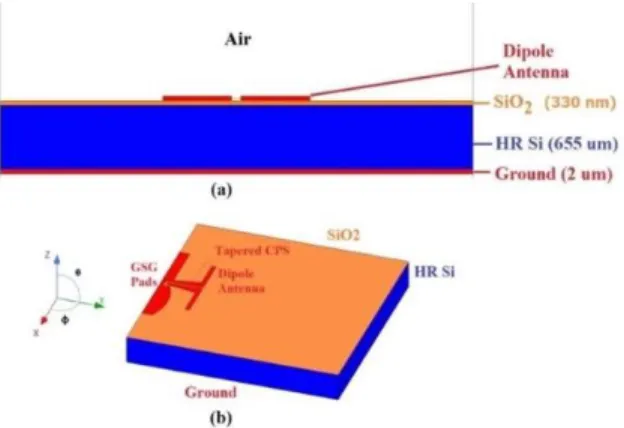
To be able to satisfy high data rate and small dimension antennas, the use of Extremely High Frequency (EHF) band (30-300 GHz) as the frequency range for propagation is investigated in this work. This choice leads to high data rates due to the high bandwidths expected. It is also interesting for the reduction of the size of the antenna due to the wavelength decrease. In order to validate the EM-Simulation, we have realized antennas in Ka band (26-40 GHz).
Based on the architecture retained (Fig. 2) and to limit the complexity of the environment, we have studied the simplest propagation channel model on a simplified CMOS structure. It consists of printed dipole antennas as they are adequate to the WiNoC in broadcast applications (omnidirectional radiation pattern and simple design). The antennas were designed based on CMOS-like Structure with grounded High Resistivity silicon (HR-Si) with: a relative permittivity εr = 11.9, a resistivity of ρ = 2.5 kΩ.cm and a thickness:
Hsub = 655 μm. A small layer of 330 nm of SiO2 (εr = 4) is
placed on the top level as an isolation. The dipole’s length is close to Ld = λg/2, with λg is the guided wavelength. The
layer and the design of dipole antenna are presented in Fig. 2. In order to facilitate the probe measurements a transition between GSG (Ground Signal Ground) pads and the dipole antenna has been designed.
Fig. 2: Design of dipole antenna: (a) stack layer; (b) 3D view of dipole antenna with feeding transition
The test structures have been realized at the Laboratory of GREMAN in Tours – France, based on the procedure explained in [23]. The measurements have been done at the Lab-STICC laboratory in Brest – France using a probe station.
The results presented in Fig. 3 and Fig. 4 show a good agreement between the simulations (on the EM simulation Software HFSSTM) and the measurement results which validate the EM-simulation tools and modeling.
The matching of the antennas is presented Fig. 3. In both cases measurement and simulation, a minimum of S11= -37 dB is obtained at 37 GHz. The presence of multiple
resonance frequencies on the reflection parameter S11 is
observed. The difference between the -10 dB matching bandwidth in simulation Fh1-Fl1 = 6.3 GHz (17.4%) and in
measurement Fh2-Fl2 = 11.1 GHz (30.8%) is due to the
uncertainty on silicon losses, the antenna environment and the measurement conditions. [24]
A good agreement between the simulated and measured S12 transmission parameter is shown in Fig. 4. With a
separation between the 2 antennas of 7.5 mm, the maximum of S12 is -12.5 dB which is similar to other measurements
found in literature [2]. If we consider a variation of -3 dB in comparison of the maximum of S12 parameter, a 4 GHz
bandwidth is obtained. Notice that this band is clearly smaller than the -10 dB matching criterion previously presented.
Fig. 3: Comparison between measurement and simulation of the reflection parameter S11 of the structure
Fig. 4: Comparison between measurement and simulation of the transmission parameter S12 of the structure
Similarly to the resonances observed in adaptation case, we notice the presence of the transmission dips in the transmission parameter S12. The dips limit the -3 dB
bandwidth. They are due to a cavity effect caused by the difference of relative permittivity between the silicon and the surrounding air (11.9 vs. 1).
This interface silicon/air behaves like magnetic walls around the silicon; associated with finite dimensions, it implies destructive interferences [22]. The difference between rays traveling through different paths, mainly the path that goes directly in the air and the path that goes in the silicon also implies transmission dips.
B. EM Simulations in V band
To really highlight this phenomenon of cavity effect and multiple paths which induced dips in transmission we have conducted several EM simulations with different scenarios as depicted in Fig. 7. To clearly highlight the cavity effect, two simulation cases are compared in this section in the V band (40-75 GHz). At the end of this paragraph, a solution to overcome the negative behavior of the cavity is proposed.
As already was seen in measurement, the problem resides in the cavity formed along the silicon substrate and due to the reflections on the dielectric/air interface, the ideal case would be to consider the lateral dimensions of the dielectric substrate as infinite (i.e. radiation boundaries on the air box surrounding the substrate). In reality, the substrate will have finite dimensions and surrounded by air.
So, the 2 cases simulated and compared are:
1. Ideal scenario: Antenna on HR-Si with infinite lateral dimensions simulated using radiation boundary on the silicon substrate edges Fig. 7 1).
2. Real scenario: Antenna on HR-Si with finite lateral dimensions simulated using an air box surrounding the silicon substrate Fig. 7 2).
We have studied these scenarios considering 4 clusters of cores on a chip, and therefore 4 antennas are placed on the silicon substrate as per the Fig. 5. The distance of separation between 2 adjacent antennas is set to 10 mm (the distance between diagonal antennas is of 14.1 mm). The characteristics of the substrate were kept the same as those used in measurements in Ka band.
Fig. 5: Scenario used for the 4 antennas
The comparison between the 2 cases has been conducted on the EM SW CST Microwave Studio© (Similar results were validated on HFSS as well) and the Scattering S-parameters are presented in Fig. 6.
The reflection parameters S11 (≈Sii) (Fig. 6-a) shows a very
different behavior between the two cases. In the case (1) with infinite dimensions a single resonance corresponding to the dipole resonance is observed as well as a large matching bandwidth (BW) that extends from 42 to 74 GHz (>50%). In case of finite dimensions, multiple resonances are present and it is difficult to identify the resonance due to the dipole.
The transmission parameter between diagonal antennas S21
looks stable on a large BW in the case (1) and we can note a -3 dB BW over 30 GHz. While the chaotic parameter obtained in the case of a finite substrate dimension (2) will make the transmission impossible.
Fig. 6: S-parameters comparison for the ideal (1) and real (2) cases: (a) S11;
(b) S21; (c) S31
For the transmission parameter between adjacent antennas S31 (and its equivalents S41), the same remarks can be said as
for the diagonal transmission. Nevertheless, in the case (1), more fluctuations are observed which may limit the transmission bandwidth (multiple bands of 4 GHz around multiple frequencies are discernible). In the next section, we present a solution to avoid the cavity behavior.
C. Proposed Solution Simulations in V band
As the ideal case (1) is practically not realizable because of the limited dimensions of the chips, and to get back to this case we suggest surrounding the Silicon layer by an absorbing material layer. In this absorbing layer, the waves will be evanescent before reaching the air and thus the reflections would be reduced significantly. This proposed solution is called thereafter case (3) and is illustrated in Fig. 7-3. We can see in the literature propositions for absorbent materials like graphene as an example [25].
A comparison between the cases (1) and (3) have been made using EM-simulation and the S-parameters results are presented in Fig. 8. The use of an absorbing layer permits to limit the number of resonances and to obtain a smooth variation like the infinite dimensions case. The contribution of the EM-absorbent can also be shown on the electric field distribution as depicted in Fig. 9. The fields’ cartography in the case (2) seems chaotic, a huge number of modes interfere which is typical of an oversized cavity while in the case (3) fields distribution can be compared to the propagation in an infinite environment.
Lower levels of transmission are observed between adjacent antennas than between the diagonal antennas despite that the separation distance is higher for the diagonal antennas than for the adjacent ones. This is due to the radiation pattern of the grounded dipole antenna which presents lower gain in the adjacent antenna’s direction than in the diagonal antenna’s direction. Nevertheless, the proposed solution helps to bypass the silicon substrate problems. To avoid this directivity problem, a solution is to use monopole antennas placed inside the silicon substrate.
D. EM Simulations for Monopole Antennas in Sub-THz band
As can be seen in the above paragraph, the antenna directivity and placement plays an important role in improving the transmission for the WiNoC channel. This hypothesis was studied in [17], [26], [27]. But in each of these publications no deep EM analysis was provided.
Fig. 8: S-parameters comparison for the ideal (1) and the solution (3) cases: (a) S11; (b) S21; (c) S31
Fig. 9: Fields distribution in the cases (2) and (3) in V band
As broadcast applications are addressed, omnidirectional vertical monopoles are good candidates [28]. In order to have a reasonable height compared to the substrate height, these monopoles have been designed in the Sub-THz band (at 200 GHz on silicon the wavelength is of ≈435μm, so a quarter-wavelength monopole would be after optimization of ≈143μm height excited by a coaxial cable conform with their dimensions) as it is presented Fig. 10. These monopoles could be metallic if the technology permits, otherwise carbon nanotubes could be integrated [29], [30], [31].
Fig. 10: Monopole geometry for 200 GHz
EM simulation has been done considering a Silicon substrate surrounded by an absorbing layer as explained previously. The distance of separation between 2 adjacent antennas is set to 10 mm and between the diagonal antennas would be 14.1 mm.
The simulations have been conducted on HFSSTM and the results of S-parameter are shown in Fig. 11 for the reflection parameter and in Fig. 12 for the transmission parameters.
A good matching (S11<-20db) is obtained and the -10 dB
bandwidth is extended to 62 GHz which represents a relative band of 31%.
As for the transmission parameters S21 & S31, we can see
fluctuations that stay in a level between -25 and -35 dB. This behavior may be explained by the multiple reflections vertically through the layers [32] [33] than by the horizontal reflections on the edges and borders of the substrate interfaces. The use of omnidirectional antennas implies higher transmission between the adjacent antennas than the diagonal antennas as the adjacent antennas are closer.
However, using high carrier frequency implies lower transmission levels for a same distance. This is due to the FRIIS equation who expresses the ratio of received power Pr to
transmitted power Pt in 3D space as:
(1) Where Gt and Gr represent the antenna gains, D is the
separating distance between the two elements and is the wavelength and is the channel attenuation. So, the greater the frequency, the lower is this ratio.
Fig. 11: S11 parameter for the monopole antenna
To evaluate the channel behavior in time domain, the S parameters obtained by measurements or EM simulations have been used in a very simple circuit modeling to obtain the eye diagram characteristics. This part is presented in the next section.
IV. TIME DOMAIN ANALYSIS OF THE PROPAGATION CHANNEL
A. Transceiver Design and Time Domain Simulations in Ka Band
To assess the channel performances, we have used the block diagram of a simple OOK transceiver shown in Fig. 13. The transmitter consists of a binary sequence generator and a sine wave generator multiplexed in an OOK modulator. The channel is formed by the touchstone file (.sNp) extracted from the measurements or the EM simulation between 2 or more antennas. The receiver includes a Low Noise Amplifier (LNA) of variable gain G and an envelope detector to recover the signal. Eye diagrams help us to check the state of the signal after each step and precisely at the receiver side.
The specific advantage of this transceiver is besides its simple design, the absence of a power amplifier at the transmitter side which will help us later to decrease the power consumption.
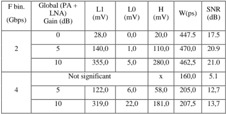
Based on the above design, the performances of the measured Ka band channel have been evaluated using ADS© circuit simulator. The aim of this simple study is to estimate the Signal to Noise Ratio (SNR) in several configurations of binary rate and amplifier gain. The noise figure of the LNA have been set arbitrarily at 10 dB and the filter of the envelop detector is simply modeled by RC cells. The simulation results are summarized in the Table 1. The representation of the 1V level: L1, the 0V level: L0, the height H and the width
W are presented in Fig. 14. The SNR is estimated using:
(2) Where d1 and d0 are the noise levels for L1 and L0
respectively (also illustrated on Fig. 14).
The SNR depends both on the binary rate Fbin and on the
global gain G of the transmission chain. The higher the data rate Fbin is, the higher the global gain G should be and thus
the higher the power consumption.
Fig. 13: Electric circuit for OOK simulation and eye diagram modeling
Fig. 14: Basic parameters obtained on ADS for the channel evaluation Table 1: Main parameters of the Eye Diagram of the measured channel in Ka band F bin. (Gbps) Global (PA + LNA) Gain (dB) L1 (mV) L0 (mV) H (mV) W(ps) SNR (dB) 2 0 28,0 0,0 20,0 447.5 17.5 5 140,0 1,0 110,0 470,0 20.9 10 355,0 5,0 280,0 462,5 21.0 4 Not significant x 160,0 5.1 5 122,0 6,0 58,0 205,0 12,7 10 319,0 22,0 181,0 207,5 13,7
In Ka band, based on the channel measurements results, we set the carrier frequency to 35 GHz, for a data rate of 2 Gbps, no global gain implies an SNR of around 17 dB which seems sufficient for WiNoC applications [5].For a data rate of 4 Gbps, the global gain needed to obtain an SNR greater than 12 dB is around 5 dB. In both binary rate cases, the use of 10 dB global gain ensures a good level of SNR implying a bit error rate lower than 10-12 which is adequate for WiNoC applications.
B. Time Domain Simulations in the mm Wave Band
Based on the EM simulations, we use here the same transceiver design used earlier for the measurement in Ka band, to realize the time domain simulations for the case (3) in mm Wave band for the monopole antennas designed with a surrounding absorbing layer and a carrier frequency of 200 GHz.
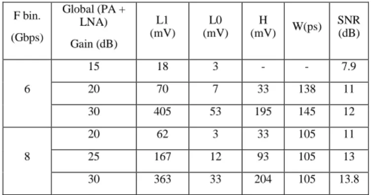
The results of the eye diagram simulations are resumed in the Table 2 and Table 3 corresponding respectively to the adjacent antennas transmission case (10 mm distance) and the diagonal antennas transmission case (14.1 mm distance). The noise figure of the different amplifiers is set to 10 dB.
Due to the Friis relation, using higher frequencies implies the need of a greater amplifier gain. This is why to achieve a data rate greater than 4 Gbps, it is necessary to use at least a global gain of 15 dB; the greater the data rate, the higher the gain needed. As an example, if 8 Gbps is needed, a global gain of 25 dB minimum is required to achieve a SNR > 9dB.
The ripple of the S-parameters limits the band, while if the response is flat, higher data rates are possible. This drawback can be compensated by using a numerical equalizer as it has a limited power consumption compared to the analog part. The lower the transmission parameters level, the higher the global gain in the chain must be.
Table 2: Eye diagram characteristics for adjacent antenna transmissions in the mm Wave band F bin. (Gbps) Global (PA + LNA) Gain (dB) L1 (mV) L0 (mV) H (mV) W(ps) SNR (dB) 6 15 18 3 - - 7.9 20 70 7 33 138 11 30 405 53 195 145 12 8 20 62 3 33 105 11 25 167 12 93 105 13 30 363 33 204 105 13.8
Table 3: Eye diagram characteristics for diagonal antenna transmissions in the mm Wave band F bin. (Gbps) Global (PA + LNA) Gain (dB) L1 (mV) L0 (mV) H (mV) W(ps) SNR (dB) 6 15 7 1 - - 7 20 50 5 7 110 8.6 30 330 37 140 130 11,5 8 20 Not significant 25 124 10 36 100 9.5 30 283 32 108 101 9,1 V. DISCUSSIONS
In this study we first observe that reflections and cavity effects must be considered to build a realistic WiNoC. We show that an absorption layer is required to get a workable solution and to avoid intractable placement constraints. Moreover considering technology constraints and cost, it is crucial that this layer is CMOS compliant. Another well identified issue is the channel uniformity with horizontal dipole antenna. We show that vertical quarter-wavelength monopole is a possible solution in the Sub-THz Band that can be integrated in a 200μm silicon layer.
The second point is related to power consumption, which is one of the main impediments to WiNoC implementation. PA and LNA are of the most significant sources of power consumption. PA efficiency is extremely low (17% in [34]) and worse than LNA. Recent work in 45nm show very impressive power gain for PA [34] and LNA[35], namely 3.9 and 1.3mw respectively, and the LNA efficiency is three times better (0.08 vs 0.24pJ/bit). So, we explore the possibility to get rid of the PA. Our simulations show that a 25dB gain provides 8 Gbps data rate for a 9.5dB SNR, which is enough to retrieve the information with a simple transmission scheme. If we assume a classic linear power model with respect to the gain, we can perform rough estimations. Let’s consider a solution without a PA and with an LNA only from [34]. We must increase the gain of the LNA from 16 to 25dB, which means a power consumption of about 2mW. This estimation must be compared to 5.2mW that is required for the LNA and PA case and a global gain of 32dB. On the contrary, note that if we consider a solution with a single PA from [34], we must
increase the gain of the PA from 16 to 25dB and obtain a power consumption of about 6mW. So, it seems to be possible to use an LNA only, this is a promising perspective since significantly lower power consumption means possible implementation and scalability. In other words, we can expect WiNoC with a significant number of routers.
Thirdly, let’s consider the frequency Band. 200GHz allows designing vertical antennas but the drawback is the energy efficiency that decreases proportionally with the frequency. Compared to 60GHz, we get a loss of about 6dB, however it is already included in our simulation scheme and in our results. Moreover digital communications methods can additionally be applied to reduce power with lower SNR. This option is motivated by the power consumption of the digital part, which is an order of magnitude lower than the analog part. Basically, we can expect to introduce Direct Sequence Spread-Spectrum
(DSSS) [36] with low spread factor and Error-Correcting
Codes (ECC) [37] techniques with high code ratio in order to maintain high data rates. Finally, digital equalization [36] can also be used to improve the bandwidth and so the data rate.
VI. CONCLUSION
Our study highlights the crucial need for realistic channel models that consider cavity effects and multi-paths. However, it also shows that WiNoC remains a promising alternative to prohibitive wired multi-hops paths and to provide efficient broadcast capabilities if appropriate design, frequency band, absorbing layer, antenna design and digital processing techniques are applied.
The immediate perspectives are firstly an analytical accurate channel model, thus we are currently running time-consuming simulations. Then we intend to provide the details and the experimental results of the CMOS-compliant absorbing layer that was briefly introduced in this paper. Finally, we intend to combine accurate RF models and digital techniques to evaluate the consistency of the complete proposed solution.
ACKNOWLEDGMENT
The authors would like to thank the "Laboratoires d'Excellence" COMINLABS and the TECHYP (the High Performance Computing Cluster of the Lab-STICC).
REFERENCES
[1] A. Mineo, M. Palesi, G. Ascia, and V. Catania, “An adaptive transmitting power technique for energy efficient mm-wave wireless NoCs,” in 2014 Design, Automation & Test in Europe Conference & Exhibition (DATE), 2014, pp. 1–6.
[2] S. Deb, A. Ganguly, P. P. Pande, B. Belzer, and D. Heo, “Wireless NoC as Interconnection Backbone for Multicore Chips: Promises and Challenges,” IEEE Journal on Emerging and Selected Topics in Circuits and Systems, vol. 2, no. 2, pp. 228–239, Jun. 2012.
[3] Y. P. Zhang, Z. M. Chen, and M. Sun, “Propagation Mechanisms of Radio Waves Over Intra-Chip Channels With Integrated Antennas: Frequency-Domain Measurements and Time-Domain Analysis,” IEEE Transactions on Antennas and Propagation, vol. 55, no. 10, pp. 2900– 2906, Oct. 2007.
[4] “Présentation - CominLabs.” [Online]. Available: https://bbc.cominlabs.u-bretagneloire.fr/.
[5] A. Karkar, T. Mak, K.-F. Tong, and A. Yakovlev, “A Survey of Emerging Interconnects for On-Chip Efficient Multicast and Broadcast in Many-Cores,” IEEE Circuits and Systems Magazine, vol. 16, no. 1, pp. 58–72, 2016.
[6] W. Hwang et al., “3D nanosystems enable embedded abundant-data computing: special session paper,” presented at the ESWEEK 2017, Seoul, South Korea, 2017, pp. 1–2.
[7] K. Ohashi et al., “On-Chip Optical Interconnect,” Proceedings of the IEEE, vol. 97, no. 7, pp. 1186–1198, Jul. 2009.
[8] Y. C. M. Boussougou, T. le Gouguec, Y. Quere, D. le Berre, P. M. Martin, and F. Huret, “Electromagnetic analysis of RF interconnect,” presented at the SPI 2008, Dublin City University, Ireland, 2008, pp. 1– 4.
[9] T. Kikkawa, “Wireless inter-chip interconnects,” Microelectronic Engineering, vol. 88, no. 5, pp. 767–774, May 2011.
[10] N. Miura, D. Mizoguchi, M. Inoue, T. Sakurai, and T. Kuroda, “A 195-Gb/s 1.2-W Inductive Inter-Chip Wireless Superconnect With Transmit Power Control Scheme for 3-D-Stacked System in a Package,” IEEE Journal of Solid-State Circuits, vol. 41, no. 1, pp. 23–34, Jan. 2006. [11] J. Lee, Y. Chen, and Y. Huang, “A Low-Power Low-Cost
Fully-Integrated 60-GHz Transceiver System With OOK Modulation and On-Board Antenna Assembly,” IEEE Journal of Solid-State Circuits, vol. 45, no. 2, pp. 264–275, Feb. 2010.
[12] F. Zhu et al., “A Low-Power Low-Cost 45-GHz OOK Transceiver System in 90-nm CMOS for Multi-Gb/s Transmission,” IEEE Transactions on Microwave Theory and Techniques, vol. 62, no. 9, pp. 2105–2117, Sep. 2014.
[13] S. Moghadami, F. Hajilou, P. Agrawal, and S. Ardalan, “A 210 GHz Fully-Integrated OOK Transceiver for Short-Range Wireless Chip-to-Chip Communication in 40 nm CMOS Technology,” IEEE Transactions on Terahertz Science and Technology, vol. 5, no. 5, pp. 737–741, Sep. 2015.
[14] C. W. Byeon, C. H. Yoon, and C. S. Park, “A 67-mW 10.7-Gb/s 60-GHz OOK CMOS Transceiver for Short-Range Wireless Communications,” IEEE Transactions on Microwave Theory and Techniques, vol. 61, no. 9, pp. 3391–3401, Sep. 2013.
[15] A. Triantafyllou et al., “High transmission performance integrated antennas on SOI substrate for VLSI wireless interconnects,” in Proceedings of the IEEE 2005 International Interconnect Technology Conference, 2005., 2005, pp. 80–82.
[16] K. Kim and others, “Characteristics of integrated dipole antennas on bulk, SOI, and SOS substrates for wireless communication,” in Interconnect Technology Conference, 1998. Proceedings of the IEEE 1998 International, 1998, pp. 21–23.
[17] E. Tavakoli, M. Tabandeh, and S. Kaffash, “An optimized phased-array antenna for intra-chip communications,” in 2011 Loughborough Antennas Propagation Conference, 2011, pp. 1–4.
[18] M. Sun, Y. P. Zhang, G. X. Zheng, and W. Y. Yin, “Performance of Intra-Chip Wireless Interconnect Using On-Chip Antennas and UWB Radios,” IEEE Transactions on Antennas and Propagation, vol. 57, no. 9, pp. 2756–2762, Sep. 2009.
[19] P. Benech, F. Ndagijimana, A. Triantafyllou, A. Farcy, and J. Torres, “Design and performance of integrated antennas for wireless intra chip interconnections,” in IECON 2006 - 32nd Annual Conference on IEEE Industrial Electronics, 2006, pp. 2953–2957.
[20] M. Bialkowski and A. Abbosh, “Investigations into intrachip wireless interconnection for ultra large scale integration technology,” in 2009 IEEE Antennas and Propagation Society International Symposium, 2009, pp. 1–4.
[21] Y. Liu, V. Pano, D. Patron, K. Dandekar, and B. Taskin, “Innovative propagation mechanism for inter-chip and intra-chip communication,” in
2015 IEEE 16th Annual Wireless and Microwave Technology Conference (WAMICON), 2015, pp. 1–6.
[22] H. M. Cheema and A. Shamim, “The last barrier: on-chip antennas,” IEEE Microwave Magazine, vol. 14, no. 1, pp. 79–91, Jan. 2013. [23] R. Allanic et al., “Three-state Microwave Tunable Resonator Integrating
Several Active Elements on Silicon Technology in a Global Design,” IEEE Microw. Wirel. Components Lett, 2018.
[24] I. E. Masri, T. L. Gouguec, P. M. Martin, R. Allanic, and C. Quendo, “Integrated dipole antennas and propagation channel on silicon in Ka band for WiNoC applications,” in 2018 IEEE 22nd Workshop on Signal and Power Integrity (SPI), 2018, pp. 1–4.
[25] B. Wu et al., “Experimental demonstration of a transparent graphene millimetre wave absorber with 28% fractional bandwidth at 140 GHz,” Scientific Reports, vol. 4, no. 1, May 2015.
[26] H. K. Mondal, S. H. Gade, M. S. Shamim, S. Deb, and A. Ganguly, “Interference-Aware Wireless Network-on-Chip Architecture Using Directional Antennas,” IEEE Transactions on Multi-Scale Computing Systems, vol. 3, no. 3, pp. 193–205, Jul. 2017.
[27] A. Mineo, M. Palesi, G. Ascia, and V. Catania, “Exploiting antenna directivity in wireless NoC architectures,” Microprocessors and Microsystems, vol. 43, pp. 59–66, Jun. 2016.
[28] W. Rayess, D. W. Matolak, S. Kaya, and A. K. Kodi, “Antennas and Channel Characteristics for Wireless Networks on Chips,” Wireless Personal Communications, vol. 95, no. 4, pp. 5039–5056, Aug. 2017. [29] S. Demoustier, E. Minoux, M. Le Baillif, M. Charles, and A. Ziaei,
“Review of two microwave applications of carbon nanotubes: nano-antennas and nano-switches,” Comptes Rendus Physique, vol. 9, no. 1, pp. 53–66, Jan. 2008.
[30] Yi Huang, Wen-Yan Yin, and Qing Huo Liu, “Performance Prediction of Carbon Nanotube Bundle Dipole Antennas,” IEEE Transactions on Nanotechnology, vol. 7, no. 3, pp. 331–337, May 2008.
[31] S. Abadal, E. Alarcón, A. Cabellos-Aparicio, M. Lemme, and M. Nemirovsky, “Graphene-enabled wireless communication for massive multicore architectures,” IEEE Communications Magazine, vol. 51, no. 11, pp. 137–143, Nov. 2013.
[32] V. Pano, I. Yilmaz, Y. Liu, B. Taskin, and K. Dandekar, “Wireless Network-on-Chip analysis of propagation technique for on-chip communication,” in 2016 IEEE 34th International Conference on Computer Design (ICCD), 2016, pp. 400–403.
[33] X. He, J. Li, M. Zhang, and S. Qi, “Improvement of integrated dipole antenna performance using diamond for intra-chip wireless interconnection,” in 2010 IEEE International Conference on Integrated Circuit Design and Technology, 2010, pp. 248–251.
[34] T. Shinde, S. Subramaniam, P. Deshmukh, M. M. Ahmed, M. Indovina, and A. Ganguly, “A 0.24pJ/bit, 16Gbps OOK Transmitter Circuit in 45-nm CMOS for Inter and Intra-Chip Wireless Interconnects,” 2018, pp. 69–74.
[35] S. Subramaniam, T. Shinde, P. Deshmukh, M. S. Shamim, M. Indovina, and A. Ganguly, “A 0.36pJ/bit, 17Gbps OOK receiver in 45-nm CMOS for inter and intra-chip wireless interconnects,” 2017, pp. 132–137. [36] J. Ortiz Sosa, O. Sentieys, and C. Roland, “A Diversity Scheme to
Enhance the Reliability of Wireless NoC in Multi-Path Channel Environment,” presented at the 12th IEEE/ACM Int. Symposium on Networks-on-Chip (NOCS 2018), Torino, Italy, 2018.
[37] A. Ganguly, P. Pande, B. Belzer, and A. Nojeh, “A Unified Error Control Coding Scheme to Enhance the Reliability of a Hybrid Wireless Network-on-Chip,” in 2011 IEEE International Symposium on Defect and Fault Tolerance in VLSI and Nanotechnology Systems, 2011, pp. 277–285.