HAL Id: pastel-00683079
https://pastel.archives-ouvertes.fr/pastel-00683079
Submitted on 27 Mar 2012HAL is a multi-disciplinary open access archive for the deposit and dissemination of sci-entific research documents, whether they are pub-lished or not. The documents may come from teaching and research institutions in France or
L’archive ouverte pluridisciplinaire HAL, est destinée au dépôt et à la diffusion de documents scientifiques de niveau recherche, publiés ou non, émanant des établissements d’enseignement et de recherche français ou étrangers, des laboratoires
Shivam Bhasin
To cite this version:
Shivam Bhasin. Logic-Level Countermeasures to Secure FPGA based Designs. Cryptography and Security [cs.CR]. Télécom ParisTech, 2011. English. �pastel-00683079�
Doctorat ParisTech
T H È S E
pour obtenir le grade de docteur délivré par
TELECOM ParisTech
Spécialité « Électronique et Communication »
présentée et soutenue publiquement parShivam BHASIN
le 14 Décembre 2011Contremesures au niveau logique pour
sécuriser les architectures de
crypto-processeurs dans un FPGA
Directeur de thèse : Jean-Luc DANGER Co-encadrement de la thèse : Tarik GRABA
Jury
M. François-Xavier STANDAERT,Professeur, UCL, Belgique Président
M. Viktor FISCHER,Professeur, ENSM SE, France Rapporteur
Mme. Ingrid VERBAUWHEDE,Professeur, KUL, Belgique Rapporteur
M. Habib MEHREZ,Professeur, UPMC, France Examinateur
Modern field programmable gate arrays (FPGA) are capable of implementing complex system on chip (SoC) and providing high performance. Therefore, FP-GAs are finding wide application. A complex SoC generally contains embedded cryptographic cores to encrypt/decrypt data to ensure security. These crypto-graphic cores are computationally secure but their physical implementations can be compromised using side channel attacks (SCA) or fault attacks (FA). This thesis focuses on countermeasures for securing cryptographic cores on FPGAs. First, a register-transfer level countermeasure called “Unrolling” is proposed. This hiding countermeasure executes multiple rounds of a cryptographic al-gorithm per clock which allows deeper diffusion of data. Results show excel-lent resistance against SCA. This is followed by dual-rail precharge logic (DPL) based countermeasures, which form a major part of this work. Wave dynamic differential logic (WDDL), a commonly used DPL countermeasure well suited for FPGAs is studied. Analysis of WDDL (DPL in general) against FA revealed that it is resistant against a majority of faults. Therefore, if flaws in DPL namely early propagation effect (EPE) and technological imbalance are fixed, DPL can evolve as a common countermeasure against SCA and FA. Continuing on this line of research we propose two new countermeasures: DPL without EPE and Balanced-Cell based DPL (BCDL).
Finally advanced evaluation tools like stochastic model, mutual information and combined attacks are discussed which are useful when analyzing counter-measures.
This PhD has been performed in the auspices of group SEN (Systèmes Élec-tronique Numérique) of Department COMELEC (Communications & Électron-ique) of Telecom-ParisTech. During these three years of graduate studies, I have learned the essence of research and development. This has been possible by working and interacting with a group of very intelligent, resourceful and kind personalities. Surely without them, my stay in Telecom-ParisTech would not be as fruitful.
First and foremost,I extend my utmost thankfulness to my PhD director, Profes-sor Jean-Luc Danger for his guidance and encouragement. His experience and expertise in the subject are matchless. Having a highly diverse knowledge base, his suggestions were of immense importance. He was of great help in getting out of many complex circumstances.
I would like to express my most sincere gratitude to Dr. Sylvain Guilley, who showed confidence in me and gave me numerous advice in academics, research and career. He is a person of great scientific acumen and admirable human values. He was by my side throughout the three years and taught me how to find paths in the dark alleys of research.
I am extremely thankful to my Co-adviser, Dr. Tarik Graba, for his guidance through various lengthy and productive discussions on the subject. His pro-found knowledge and extensive experience along with his helping nature proved to be a treasure for me. I take great pride in having worked with these three gentlemen, who are the specialists in the domain of Cryptography and Security. I have learned a lot from them.
I am also thankful to Professor Francois-Xavier Standaert for accepting me as an intern in his team at UCL, Belgium for a period of three months. His profound knowledge in the feild of side-channel analysis helped me learn a lot and widen my research perspectives.
approved by such well renowned specialists.
The moments spent with many peers is perhaps one of the best memories that I will take with me of my graduate studies. I cherish all the moments of stress and joy spent with my collegues Nidhal, Olive (Olivier), Joe (Youssef ), Fhal (Houssem), Max (Maxime), Taufeek, Seb (Sebastian), Zizou (Aziz), Zouha, Nicholas, Amel, Florent, Chantal, Daniel, Zouina and Laurent. I specially admire the efforts of Olivier which he took to teach me french. I have very much enjoyed being in the company of friends like Babu (Sumanta), Shady (Chadi), Mirani (Farhan), Hasham, Mayassa, Marcel, Paulo, Francesco, Lauriane, Nora, Davi, Gutemberg, Khalil, Waqqas, Sami, Tushar, Arif and the list goes on and on. The various ecsapades in Paris with Shady (Chadi), Babu (Sumanta), Hasham and Mirani (Farhan) goes into my ROM.
I am most fortunate to have my family: my parents, my grandmother and sister. Their constant encouragement has pushed me to be the best that I can be. I am certain that this work has been a product of my family’s love and support throughout my life.
Last but not the least I am thankful to The French National Research Agency (ANR), who financed this thesis through theANR-07-ARFU-010grant “SeFPGA” (Secured Embedded FPGAs). I would also like to thank the DGA project “Rapid BCDL” for its support.
Abstract iii
List of Figures xi
List of Tables xv
Glossary xvii
Résumé Français xix
1 Introduction 1 1.1 Motivation . . . 1 1.2 Organization . . . 2 1.3 Contributions . . . 4 2 General Background 5 2.1 Modern Cryptography . . . 6
2.2 Symmetric Key Cryptography . . . 7
2.2.1 Data Encryption Standard . . . 9
2.2.2 Advanced Encryption Standard . . . 10
2.3 Public-Key Cryptography . . . 12
2.3.1 RSA . . . 13
2.3.2 Elliptic Curve Cryptography . . . 13
2.4 Physical Cryptanalysis . . . 14
2.4.1 Fault Attacks . . . 15
2.4.2 Side Channel Attacks . . . 18
2.5 Side Channel Attack Model & Distinguisher . . . 20
2.5.1 Leakage Model . . . 20
2.5.2 Simple Power Analysis . . . 21
2.5.4 Correlation Power Analysis . . . 22
2.5.5 Mutual Information Analysis . . . 23
2.6 Need for Countermeasures . . . 24
2.6.1 Countermeasures against FA . . . 25
2.6.2 Countermeasures against SCA . . . 29
2.7 Field Programmable Gate Arrays . . . 33
2.7.1 Generic FPGA Design Flow . . . 35
3 Protecting Cryptographic Circuits at the RTL Level 37 3.1 Protecting Cryptographic Implementations at the Component Level . . . 38
3.1.1 AES Co-processor . . . 38
3.1.2 Experimental setup and data acquisition . . . 41
3.1.3 Cost Comparison of the Three AES Architectures . . . 43
3.1.4 Security Evaluation of the Three AES Architectures against SCA . . . 44
3.1.5 Security Evaluation of the Three AES Architectures against FA . . . 44
3.1.6 Discussion . . . 50
3.2 Unrolling Cryptographic Circuits as a Countermeasure . . . 51
3.2.1 Rationale of the Countermeasure . . . 51
3.2.2 Fully unrolled DES implementation on ASIC . . . 53
3.2.3 Security Evaluation of the Proposed Countermeasure . . . 56
3.2.4 Attack on the Unrolled DES . . . 59
3.2.5 Evaluation Based on Mutual Information Metric . . . 62
3.3 Conclusions . . . 63
4 DPL Countermeasures for FPGA 65 4.1 Dual-Rail with Precharge Logic . . . 66
4.1.1 Dual-Rail with Precharge Logic Protocol . . . 66
4.1.2 DPL Flaw: Early Propagation Effect . . . 67
4.1.3 DPL Flaw: Technological Imbalance . . . 69
4.2 Wave Dynamic Differential Logic . . . 69
4.2.1 Basic theory of WDDL . . . 69
4.2.2 Design Flow for WDDL Implementation on FPGA . . . 71
4.2.3 WDDL Implementation and Synthesis Results . . . 72
4.3 Security Evaluation of WDDL against SCA . . . 74
4.4 Security Evaluation of WDDL against FA . . . 74
4.4.2 Theoretical Fault Analysis . . . 78
4.5 DPL: State of the Art . . . 85
4.5.1 WDDL Variants . . . 86 4.5.2 SDDL . . . 90 4.5.3 Partial DDL . . . 91 4.5.4 MDPL . . . 92 4.5.5 DRSL . . . 92 4.5.6 STTL . . . 96 4.5.7 DPL styles Comparison . . . 96
4.6 Security Evaluation of DPL against FA . . . 98
4.6.1 Fault Model . . . 98
4.6.2 Faults Transformation . . . 99
4.6.3 Propagation of NULL Values Through Substitution Boxes . . . .101
4.6.4 Analysis of the FA Protection of DPL . . . .101
4.6.5 Low-cost countermeasure against setup time violation attacks . . . .105
4.7 Conclusions . . . .106
5 Novel DPL countermeasures for FPGA 109 5.1 DPL without Early Propagation Effect (DPL w/o EPE) . . . .109
5.1.1 Rationale of the Proposed Logic . . . .109
5.1.2 Implementation on FPGA . . . .113
5.1.3 Evaluation of Early Propagation Effect . . . .115
5.1.4 Balanced Placement . . . .119
5.1.5 Evaluation of Balanced Placement . . . .120
5.2 Balanced-Cell Based Dual-Rail Logic (BCDL) . . . .120
5.2.1 Synchronization to counter EPE . . . .125
5.2.2 Area Optimization . . . .128
5.2.3 Performance Optimization . . . .130
5.2.4 Implementation of AES BCDL on FPGA . . . .130
5.2.5 Improving AES BCDL to reduce routing imbalance on FPGA . . . .136
5.2.6 Security Evaluation of BCDL against SCA on Altera Stratix II . . . .139
5.2.7 Initial Results on Xilinx Virtex V FPGA . . . .142
6 Advanced Evaluation Techniques 149
6.1 Evaluation Tools for DPL Implementations . . . .150
6.1.1 Template Attacks . . . .150
6.1.2 Stochastic Model Attack . . . .151
6.1.3 Experimental Results . . . .152 6.1.4 Discussion . . . .156 6.2 Combination of Measurements . . . .156 6.2.1 Theoretical Background . . . .157 6.2.2 Practical results . . . .159 6.3 Conclusions . . . .162
7 Conclusion and Perspectives 165 7.1 Summary . . . .165
7.2 Perspectives . . . .167
List of Publications 169
1 Une cellule logique de base dans un FPGA . . . xix
2 Logic cluster. . . xx
3 Différentes attaques par canaux auxiliaires . . . xx
4 Différentes attaques par injection de fautes . . . xxi
5 Une S-box masquée en logiciel . . . .xxii
6 Exemple d’algorithme cryptographique iteratif et "unrolled". . . .xxiii
7 Chronogramme d’une porte ET dans le WDDL. . . .xxiii
8 Conversion d’un circuit numérique classique en WDDL. . . .xxiv
9 Comparaison de DPL w/ EPE et DPL w/o EPE par MIA. . . .xxvii
10 Cellule BCDL à n-entrées. . . .xxvii
11 BCDL S-box. . . .xxix
12 Traces MIA pour la comparaison de trois implémentations d’AES. . . .xxx
13 Estimation de l’MI par “templates”, MIA et modèle stochastique. . . .xxxi
14 Localisation de fuites . . . .xxxii
15 Placement d’antennes pour l’attaque combinée. . . .xxxii
2.1 Data Encryption Standard . . . 10
2.2 Fault effect on round 9 of AES. . . 18
2.3 Fault effect on round 8 of AES . . . 19
2.4 Basic CMOS inverter. . . 20
2.5 SPA on RSA implementation . . . 22
2.6 Parity based countermeasure . . . 25
2.7 Concurrent error detection . . . 26
2.8 Robust code countermeasure. . . 28
2.9 Double-Data-Rate as countermeasure . . . 28
2.10 S-box for masking by software. . . 31
2.12 Basic logic element in an FPGA. . . 34
2.13 Logic cluster. . . 34
2.14 Generic FPGA CAD flow. . . 35
3.1 AES architecture. . . 39
3.2 S-box as combinatorial tables in LUT. . . 40
3.3 S-box as synchronous tables in RAM. . . 40
3.4 S-box using algebraic computation in composite field (GF(24)). . . 40
3.5 Experimental attack platform. . . 41
3.6 Setup time violation caused by a permanent under-voltage. . . 42
3.7 AES faults analysis. . . 43
3.8 Occurrence of faults: s-box in GF (24). . . 45
3.9 Occurrence of faults: s-box in LUT. . . 46
3.10 Occurrence of faults: s-box in RAM. . . 46
3.11 Coverage of single faults, and detail of exploitable faults in GF (24). . . 46
3.12 Coverage of single faults, and detail of exploitable faults in LUT. . . 47
3.13 Coverage of single faults, and detail of exploitable faults in RAM. . . 47
3.14 Hamming weight of exploitable faults in GF (24). . . 47
3.15 Hamming weight of exploitable faults in LUT. . . 48
3.16 Hamming weight of exploitable faults in RAM. . . 48
3.17 Temporal localization of single faults. . . 48
3.18 Spatial localization of single faults. . . 49
3.19 Exploitable errors. . . 50
3.20 Iterative and unrolled cryptographic algorithm . . . 52
3.21 Unrolled DES Architecture. . . 54
3.22 Floorplan of DES iterative and unrolled . . . 55
3.23 TCL timing constraints for multi-cycle synthesis . . . 56
3.24 Power trace of iterative DES . . . 57
3.25 Power trace of unrolled DES . . . 57
3.26 Notations used to describe the combinatorial DES leakage functions. . . 60
3.27 DPA covariance for first s-box . . . 61
3.28 MI for iterative and unrolled DES . . . 62
4.1 The DPL protocol showing two phase operation. . . 66
4.2 DPL AND gate timing with early evaluation. . . 68
4.4 Timing diagram for a WDDL AND gate. . . 70
4.5 WDDL building block. . . 70
4.6 WDDL design flow for Altera FPGA. . . 72
4.7 Basic architecture of WDDL wrapper. . . 73
4.8 WDDL AND gate with the Early Evaluation flaw. . . 74
4.9 Occurrence of fault in (a) Single rail, (b) WDDL. . . 75
4.10 Temporal localisation of fault in (a) Single rail, (b) WDDL. . . 76
4.11 Spatial localisation of fault in (a) Singlerail, (b) WDDL. . . 76
4.12 WDDL implementation of the XOR gate. . . 80
4.13 Dual-to-single rail circuitry usable in the case of a NULL0 spacer. . . 82
4.14 Power dependence of a WDDL circuit in the faults. . . 85
4.15 Practical power consumption of a WDDL circuit in the presence of faults. . . 86
4.16 Different implementations of combinatorial function . . . 88
4.17 Timing Diagram for (a, b, c) = (0/1,1,1) . . . . 90
4.18 Timing Diagram for (a, b, c) = (0/1,0,0) . . . . 90
4.19 Pairwise balance of dual-rail pairs in a DPL netlist. . . 91
4.20 EPE prone netlist . . . 91
4.21 (a) Genuine DRSL AND gate and (b) Glitch-free variant. . . 93
4.22 Two DPL w/ EE drawbacks to fight DFAs . . . .100
4.23 Absorption of VALID faults . . . .100
4.24 Set of 2n wires that are coupled and will be subject to m faults. . . .103
4.25 Probability that m faults on n wired be innocuous . . . .104
4.26 Low-cost countermeasure against faults . . . .105
4.27 Chain Voltage/lcell. . . .106
5.1 DPL building block. . . .110
5.2 Comparison of DPL w/ EPE and DPL w/o EPE using MI . . . .116
5.3 Bitwise leakage of S − box0 in DPL w/ EPE. . . .118
5.4 Bitwise leakage of S − box0 in DPL w/o EPE. . . .118
5.5 Placement constraints on Altera . . . .120
5.6 Key value retrieved by CPA for DPL w/ EPE. . . .121
5.7 Key value retrieved by CPA for DPL w/ EPE-BB. . . .122
5.8 Key value retrieved by CPA for DPL w/o EPE. . . .123
5.9 Key value retrieved by CPA for DPL w/o EPE-BB. . . .124
5.11 n-input BCDL cell. . . .126
5.12 Temporal relationships of a 2-input BCDL OR gate signals. . . .127
5.13 Structure of T and F LUT. . . .128
5.14 Local switching balance in BCDL: LUT3 example. . . .129
5.15 A low cost DPL S-box in RAM. . . .129
5.16 Basic BCDL versus speed-optimized BCDL timings. . . .131
5.17 (a) BCDL DFF, (b) BCDL S-box. . . .132
5.18 (a) BCDL XOR, (b) BCDL Multiplexer. . . .135
5.19 Logical diagram of xtime() function. . . .137
5.20 Architecture of AES-128 datapath using T-box architecture. . . .138
5.21 XOR network used in the T-box architecture . . . .138
5.22 MI comparison for s-box 0 . . . .140
5.23 MI comparison for s-box 1 . . . .140
5.24 MI comparison for s-box 2 . . . .141
5.25 MI comparison for s-box 3 . . . .142
5.26 MI comparison using mono-bit model for s-box 0 . . . .143
5.27 Zoom on Figure5.26 . . . .144
5.28 Difference in routing in AES BCDL using s-boxes . . . .145
5.29 Difference in routing in AES BCDL using t-boxes . . . .146
6.1 MI for simulated traces with added Gaussian noise . . . .153
6.2 Examples of distributions with additive Gaussian noise. . . .154
6.3 Comparing MI estimation from templates, stochastic and MIA . . . .155
6.4 Localizing leakage using stochastic models and MIA . . . .156
6.5 Possibility of Combination . . . .159
6.6 Antenna setup for combination of measurements . . . .160
6.7 Calculation of PC . . . .161
6.8 The mechanism of combination using an aggregate functionΨ. . . .161
1 Calcul de maques pour une LUT-4 dans DPL w/ EPE . . . .xxv
2 Calcul de maques pour une LUT-4 dans DPL w/o EPE . . . .xxvi
3 Table de vérité d’une porte XOR BCDL à 2 entrées. . . .xxviii
4 Comparaison en coût et en performance pour AES BCDL . . . .xxix
5 Nombre de traces pour l’attaque combinée. . . .xxxiii
2.1 Non-linear Robust code implementation cost. . . 27
3.1 Cost comparison of the three AES architectures. . . 44
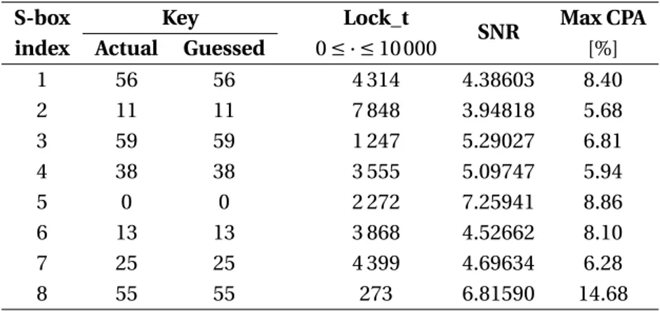
3.2 MTD for first 8 s-boxes of the three AES implementations. . . 44
3.3 Cost & Performance Comparison Iterative and Fully Unrolled DES. . . 58
3.4 CPA on iterative DES . . . 59
3.5 CPA on unrolled DES . . . 59
3.6 CPA on unrolled DES with Hamming distance model . . . 60
4.1 Area & Performance comparison of WDDL AES . . . 73
4.2 Single fault in round 10. . . 77
4.3 Single fault in round 9. . . 77
4.4 Fault strictly before round 9. . . 77
4.5 Modified functionality of an AND gate in the presence of erasure faults. . . 79
4.6 Modified functionality of an XOR gate in the presence of erasure faults. . . 79
4.7 Equations for the bytes transformations ×01, ×02 and ×03. . . 81
4.8 Truth table for the universal gateAND. . . 82
4.9 Simulation of DRSL NAND gate . . . 94
4.10 DPL performance and security features overview. . . 97
4.11 Number of NULL token through DES and AES s-box . . . .101
5.2 LUT mask for 4-input LUT in DPL w/o EPE . . . .112
5.3 LUT masks for the 2 → 1 gates in DPL w/ and w/o EE styles. . . .113
5.4 Area & Performance comparison of DPL w/o EPE . . . .115
5.5 CPA results on S-box 0 for two DPL variants of AES. . . .115
5.6 Truth Table of a 2-input BCDL XOR gate. . . .134
5.7 Cost Comparison of AES BCDL on Stratix II. . . .135
5.8 Cost & Performance Comparison of AES BCDL using T-box on Stratix II. . . . .139
5.9 Cost & Performance Analysis on Xilinx Virtex V. . . .143
Glossary
AES: Advanced Encryption Standard
ASIC: Application Specific Integrated Circuit
BCDL: Balanced Cell based Dual-rail Logic
CBC: Cipher Block Chaining
CLB: Configurable Logic Block
CPA: Correlation Power Analysis
DBA: Differential Behavioral Analysis
DDR: Double Data Rate
DES: Data Encryption Standard
DFA: Differential Fault Attack
DPA: Differential Power Analysis
DPL: Dual-rail with Precharge Logic
DPL w/ EPE: DPL with Early Propagation Effect
DPL w/o EPE: DPL without Early Propagation Effect
DRSL: Dual-rail Random Switching Logic
ECB: Electronic Code Book
ECC: Elliptic Curve Cryptography
EPE: Early Propagation Effect
EMA: Electro Magnetic Analysis
FA: Fault Attack
FIPS: Federal Information Processing Standard
FPGA: Field Programmable Gate Array
GF: Galois Field
LUT: Look-Up Table
MDPL: Masked Dual-rail Precharge Logic
MIA: Mutual Information Analysis
MTD: Minimum Traces to Disclose the key
NIST: National institute of standard and technology
RAM: Random Access Memory
RSA: Rivest Shamir Adleman
RTL: Register Transfer Logic
PC: Possibility of Combination
PKC: Public Key Cryptography
SCA: Side Channel Attack
SKC: Symmetric Key Cryptography
SPA: Simple Power Analysis
UART: Universal Asynchronous Receiver Transmitter
Le réseau de portes programmable (FPGA) est un circuit intégré qui contient des cellules logiques identiques en tant que composants standards. Chaque cellule logique peut être programmée indépendamment. Ces cellules logiques identiques sont appelées blocs logiques configurables (CLB). La Figure1montre la cellule CLB qui se compose d’une “Look- up table (LUT)"" à quatre entrées. Elle permet de mettre en œuvre toute fonction booléenne à qua-tre entrées et même une bascule active sur front pour les circuits séquentiels. Les cellules CLB individuelles sont reliées entre elles par une matrice de fils et par des commutateurs programmables.
LUT 4 FF
CLK
PRESET RESET
Figure 1: Une cellule logique de base dans un FPGA
Les FPGAs commerciales possèdent des cellules CLB plus complexes par rapport aux blocs logiques de base comme des multiplexeurs, chaînes à retenue rapide, registres en cas-cade, “Set/Reset” sur des bascules etc. Les CLBs dans un FPGA commercial sont souvent organisées de façon hiérarchique (voir la Figure 2). Les FPGAs comprennent également des macros complexes tel que des multiplieurs, des blocs DSP, RAM.
Les FPGAs ont considérablement évolués au cours de ces dernières années. Les plus modernes sont capables de mettre en œuvre un système complexe sur puce (SoC) et de fournir des performances élevées. Par conséquent, on les utilise dans un large domaine d’applications dans les circuits réels. Un complexe SoC contient généralement un noyau
LE LE N I LUT K LUT K
Figure 2: Logic cluster.
cryptographique embarqué pour chiffrer/déchiffrer des données sur le bus système et donc assurer la sécurité. Ces noyaux cryptographiques sont mathématiquement sûrs, mais leurs implémentations physiques peuvent être défaillantes.
TA
Attacked circuit
EMA
SPA, DPA, templates, etc.
Time
Figure 3: Différentes attaques par canaux auxiliaires
Figure 4: Différentes attaques par injection de fautes
physique. La première attaque physique qui a été publiée est nommée "Timing attack” qui a été présentée par Kocher et al. en 1996 [1]. Dans cette attaque, un adversaire est capable de récupérer une clé secrète utilisée dans un algorithme de signature par la violation du temps d’exécution de diverses opérations. Cette attaque est un exemple d’attaque par canaux aux-iliaires (SCA) (voir la figure3) puisque c’est entièrement passif : le système attaqué n’est pas détruit. D’autres attaques par canaux auxiliaires permettent d’espionner les propriétés du circuit comme la consommation d’énergie et le rayonnement électromagnétique [2,3]. Leur étude a mobilisé de nombreux chercheurs.
Ces attaques se déroulent en deux étapes : la collecte d’informations par canaux auxili-aires puis leurs analyses. La collecte par canaux auxiliauxili-aires est une étape de métrologie, par contre, l’étape d’analyse nécessite des outils sophistiqués théoriques pour être efficace. Ces deux aspects progressent rapidement, comme le témoigne le concours “DPA Contest” [4]. Une autre classe d’attaques physiques connues sous le nom “active” ou attaques par faute (FA, voir la figure4) fonctionne en modifiant le comportement fonctionnel du dispositif at-taqué par des perturbations [5,6]. Cette thèse porte sur les contremesures SCA et FA pour sécuriser les noyaux cryptographiques dans les FPGAs.
Jusqu’à maintenant, de nombreuses contremesures ont été conçues pour sécuriser les implémentations de systèmes cryptographiques. L’objectif principal de ces contremesures est d’éliminer toute dépendance entre les opérations internes d’un crypto-système et les fuites correspondantes. La plupart des contremesures, si ce n’est la totalité, utilise la
redon-dance pour renforcer le crypto-système contre la SCA et la FA. Ces contremesures peuvent être classées en deux catégories:
1. masquage de l’information, [7, Chap. 9], qui vise à rendre la fuite aléatoire
2. dissimulation de l’information, [7, Chap. 7], qui vise à cacher l’information secrète présente dans les canaux cachés.
Les contremesures basées sur le masquage de l’information utilisent une valeur générée aléatoirement appelée “masque” de telle sorte que la fuite corresponde au masque sans af-fecter la valeur du chiffré de sortie comme le montre la figure5. Une implémentation cor-recte d’une contre-mesure basée sur le masquage protège contre les attaques SCA de pre-mier ordre. Les attaques d’ordre supérieur peuvent néanmoins réussir.
S
m
S
x ⊕ k
S(x ⊕ k)
S(x ⊕ k) ⊕ m
x ⊕ k ⊕ m
m
Figure 5: Une S-box masquée en logiciel
Les contremesures utilisant la dissimulation d’information, comme le nom l’indique, tentent de cacher l’information de l’attaquant. La résistance de ces contremesures face aux attaques FA n’a pas été étudiée en profondeur. Dans le travail présenté, l’accent est mis sur l’étude des contremesures basées sur la dissimulation de l’information pouvant être implémentée sur un FPGA commerciale. Mon objectif est d’étudier le bien-fondé de ces contremesures, de les implémenter efficacement sur FPGA et d’effectuer une analyse sécuritaire contre les attaques SCA et FA connues dans l’état de l’art. Les contremesures sur lesquelles je me focalise sont (sous leurs dénominations anglaises): Loop Unrolling et
Dual-Rail Precharge Logic (DPL).
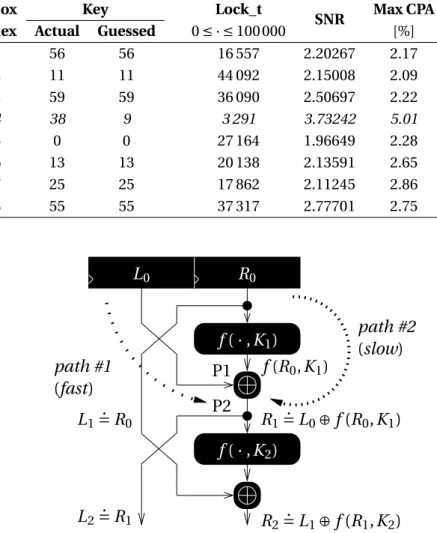
Dans un algorithme de chiffrement par bloc, les données sont chiffrées en répétant une série d’opérations et en utilisant une clef différente à chaque fois, générée à partir de
(a)
Round
K
iplaintext
clock
sequential combinatonialciphertext
(b) Round K1 Round KN ciphertext plaintext clock combinatonial ... sequentialFigure 6: (a) Architecture d’un algorithme cryptographique itératif. (b) Architecture d’un algo-rithme cryptographique totalement "unrolled".
Precharge Evaluation bT yT bF yF aF aT P RE /EV AL
Figure 7: Chronogramme d’une porte ET dans le WDDL.
la clef précédente. Cet ensemble d’opérations est appelé une tour. Le nombre de tours est choisi de telle sorte que les cryptanalyses linéaire et différentielle soient plus difficiles qu’une recherche exhaustive sur l’ensemble des clefs possibles. Les circuits cryptographiques sont généralement conçus pour effectuer soit certaines opérations, soit la tour entière en un seul cycle d’horloge comme le montre la figure6(a). L’idée du “unrolling” est d’implémenter
Single−rail Dual−rail
G
G
BT
AT
AF
B
FY
B
A
YT
YF
G
∗Figure 8: Conversion d’un circuit numérique classique en WDDL.
le circuit de telle manière que les multiples tours soient calculées en un seul cycle comme le montre la figure6(b). Il s’agit d’une contre-mesure appliquée au niveau RTL (Register Transfer Logic), ce qui la rend totalement indépendante de la plateforme utilisée. Elle peut être classée comme une contre-mesure dissimulant l’information car l’information est tou-jours présente mais d’une manière cachée. En d’autres termes, il est très difficile de trouver un modèle de fuite permettant d’exploiter l’information présente.
Une contremesure couramment utilisée pour protéger ces systèmes cryptographiques est DPL (Dual-rail Precharge Logic). La première phase de la thèse a porté sur les con-tremesures DPL proposées précédemment. WDDL (Wave Dynamic Differential Logic) est une contre-mesure DPL couramment utilisée, composée sur toute la logique positive. Elle est ainsi bien adaptée pour les FPGA. La figure8montre la conversion d’un simple circuit numérique en WDDL. Ces circuits effectuent un nombre uniforme de transitions par cy-cle, par le biais de duplications et d’opérations en deux phases (pré-charge et évaluation). Il peut être vérifiée à partir de la figure7qu’une porte AND implémentée avec le système WDDL a une consommation d’énergie très équilibrée. Non sans difficulté, il a finalement été montré que le WDDL était vulnérable aux attaques SCA. Comme indiqué dans des di-verses publications, cette vulnérabilité vient de l’effet de propagation précoce (early prop-agation effect (EPE)) et du routage déséquilibré sur le FPGA. Toutefois, WDDL a la remar-quable propriété de résister contre la majorité des fautes (fautes asymétriques). Par con-séquent, s’il existe un moyen de retirer les défauts mentionnés ci-dessus à la technologie DPL, cela peut devenir une contre-mesure commune contre les attaques SCA et FA. Ainsi
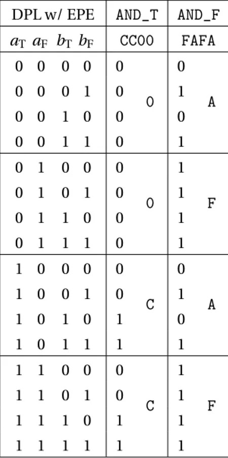
Table 1: Calcul de maques pour une LUT-4 dans DPL w/ EPE
DPL w/ EPE AND_T AND_F
aT aF bT bF CC00 FAFA 0 0 0 0 0 0 0 A 0 0 0 1 0 1 0 0 1 0 0 0 0 0 1 1 0 1 0 1 0 0 0 0 1 F 0 1 0 1 0 1 0 1 1 0 0 1 0 1 1 1 0 1 1 0 0 0 0 C 0 A 1 0 0 1 0 1 1 0 1 0 1 0 1 0 1 1 1 1 1 1 0 0 0 C 1 F 1 1 0 1 0 1 1 1 1 0 1 1 1 1 1 1 1 1
les nouvelles variantes de DPL évitant l’EPE et le déséquilibre de routage sont devenus un champ de recherche intéressant.
Pour améliorer la contremesure DPL par la contremesure DPL sans EPE en une simple modification dans la table de vérité des portes logiques de base est suffisante. Dans les FPGAs, on peut réaliser cette modification en forçant le masque de la LUT à une valeur pré-calculée. Les tableaux 1et 2montrent respectivement le calcul de masque de LUT pour la contremesure DPL normale et pour la contremesure DPL sans EPE.
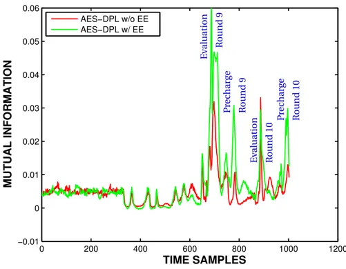
L’analyse par information mutuelle (MIA) montre que la suppression de l’effet EPE ré-duit énormément la fuite du canal auxiliaire comme le montre la figure9. Ce qui reste de la fuite provient du routage déséquilibré qui est le résultat de “fan-out” élevé des portes logiques. Il est très difficile de contrôler le routage dans les FPGAs pour les grandes con-ceptions car même si on met des contraintes de routage elles peuvent être ignorées par la plus part des outils de synthèse pendant la phase de l’optimisation. J’ai forcé le routage sur
Table 2: Calcul de maques pour une LUT-4 dans DPL w/o EPE
DPL w/o EPE AND_T AND_F Input state in
aT aF bT bF FC80 FAE0 the DPL protocol 0 0 0 0 0
0
0
0
All NULL0 0 0 0 1 0 0 Transitional from NULL0 0 0 1 0 0 0 Transitional from NULL0
0 0 1 1 0 0 Faulty
0 1 0 0 0
8
0
E
Transitional from NULL0 0 1 0 1 0 1 All VALID: (a, b) = (0,0) 0 1 1 0 0 1 All VALID: (a, b) = (0,1) 0 1 1 1 1 1 Transitional from NULL1 1 0 0 0 0
C
0
A
Transitional from NULL0 1 0 0 1 0 1 All VALID: (a, b) = (1,0) 1 0 1 0 1 0 All VALID: (a, b) = (1,1) 1 0 1 1 1 1 Transitional from NULL1 1 1 0 0 1
F
1
F
Faulty
1 1 0 1 1 1 Transitional from NULL1 1 1 1 0 1 1 Transitional from NULL1
1 1 1 1 1 1 All NULL1
l’FPGA Altera Stratix mais ce la n’a pas apporté beaucoup d’amélioration.
La deuxième contremesure est BCDL( “Balanced-cell based DPL”). Cette logique se com-posent d’un signal globale PRE qui est utilisé pour synchroniser toutes les portes ce qui élimine l’effet EPE comme le montre la figure10. L’autre avantage de l’utilisation de le BCDL est la possibilité d’utiliser les mémoires embarquées avec une taille raisonnable. Cette avan-tage réduit la taille utilisée du FPGA offre une meilleure performance et un faible "fan-out". J’ai proposé une approche "bottom-up" pour implémenter BCDL dans les FPGAs. Les ré-sultats montrent une résistance effective contre les attaques passives et les attaques actives. Le routage déséquilibré peut être encore un sujet de préoccupation qui peut être contré par la commutation de chemin.
Un algorithme cryptographique comme l’AES peut être implémenté en utilisant quatre primitives:
0 200 400 600 800 1000 1200 −0.01 0 0.01 0.02 0.03 0.04 0.05 0.06 TIME SAMPLES MUTUAL INFORMATION AES−DPL w/o EE AES−DPL w/ EE P rec har ge R ou n d 9 R ou n d 9 E v al uat ion R ou n d 10 P rec har ge R ou n d 10 E v al uat ion
Figure 9: Comparaison de le fuite de l’information mutuelle dans deux AES protégé en utilisant DPL w/ EPE et DPL w/o EPE.
at bt PRE
Bundle data
. . .
af bf sf at btT
af bfF
st. . .
. . .
U /P REFigure 10: Cellule BCDL à n-entrées.
• Multiplexeurs, • S-boxes (mémoires) • Registres (DFF).
Pour convertir un simple AES en BCDL en utilisant l’approche "bottom-up", les étapes suivante doivent être suivies:
1. Le code pour un AES avec rail unique, devrait être écrit d’une façon structurelle en utilisant des primitives. Dans le cas spécifique d’AES, ces primitives sont une bascule D, des mémoires (pour les s-box), des portes XOR et des multiplexeurs.
2. Tous les signaux de données devrait être identifiés et dupliqués. Ce qui veut dire qu’un quelconque signal s devrait être converti en deux signaux sV et sF.
3. Les quatre primitives devraient être remplacées par les primitives BCDL. Les primi-tives BCDL sont double-rail et sont soumises à deux phases d’opérations.
4. Ensuite, un adaptateur qui peut connecter des entrées/sorties simple-rail aux signaux de données double-rail est ajouté. Cet adaptateur assure aussi que les entrées/sorties sont pré-chargées à chaque coup d’horloge, ceci permet d’être conforme au protocol DPL.
5. Puisqu’un circuit DPL fonctionne à moitié fréquence d’un circuit simple-rail, la ma-chine d’état devrait fonctionner durant seulement la phase d’évaluation.
Table 3: Table de vérité d’une porte XOR BCDL à 2 entrées.
P RE I 1T I 1F I 2T I 2F OT OF 0 X X X X 0 0 1 0 0 X X 0 0 1 1 1 X X 0 0 1 X X 0 0 0 0 1 X X 1 1 0 0 1 0 1 0 1 0 1 1 0 1 1 0 1 0 1 1 0 0 1 1 0 1 1 0 1 0 0 1
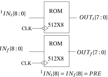
Une implémentation appropriée utilisant les mémoires et les portes XOR est cruciale quant à la sécurité de BCDL. Pour implémenter une porte XOR, le FPGA est forcé à utiliser le même modèle pré-calculé pour chaque porte XOR (table3). La figure11 montre une implémentation des mémoires qui utilisent le P RE comme bit le plus significatif de son adresse. Ainsi quand le P RE est au niveau "bas", la sortie est bloquée à “00000000” pour activer la pré-charge.
ROM
512X8
512X8
ROM
CLK
CLK
1I N
t[8 : 0]
OU T
f[7 : 0]
OU T
t[7 : 0]
I N
f[8 : 0]
1I N
t[8] = I N
f[8] = PRE
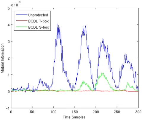
Figure 11: BCDL S-box.La DPL w/o EPE était attaquable par suite à un routage déséquilibré. Les analyses mon-trent que des registres avec un grand nombre de sorties, mais aussi un chemin critique long provoquant des fuites exploitables. A partir de ces résultats, j’ai implémenté une version d’AES BCDL dont les registres ont peu de sorties, et un chemin critique plus court. Ceci était possible grâce à la version T-box d’AES. Les T-box sont un ensemble de 8x32 tables, qui combinent le SubBytes, ShiftRows et le MixColumns. Un tour complet d’AES peut être calculé en utilisant les T-box et les portes XOR. Puisque les T-box sont des tables, elles peu-vent être implémentées sous forme de bloques mémoires dans le FPGA. Un AES basé sur les T-box partage les même primitives qu’un AES S-box, comme les mémoires, les portes XOR, les multiplexeurs et les registres. J’ai implémenté trois modèles, un AES non protégé, un AES BCDL en utilisant des S-box, finalement un AES BCDL en utilisant les T-box sur un FPGA Altera Stratix II. Les résultats de synthèses sont montrés dans la Table4. Les résultats de l’attaque MIA montrent clairement la fuite dont chacune des trois implémentation (voir figure12.
Table 4: Comparaison en coût et en performance d’implémentations AES non protégé et BCDL sous Stratix II.
Architecture Unprotected AES AES BCDL (S-box) AES BCDL (T-box)
ALUT 483 2302 2669
Registers 271 1041 1041
Figure 12: Traces MIA pour la comparaison de fuite de la S-Box 0 pour trois implémentations d’AES.
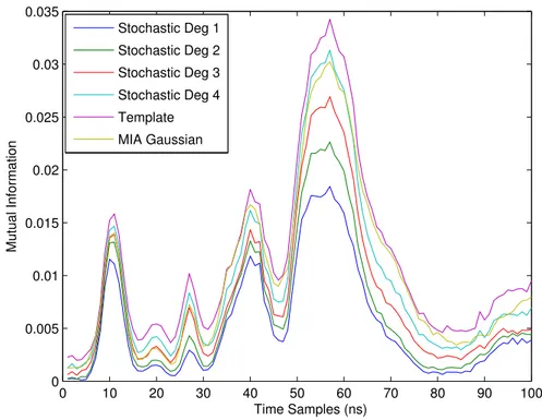
J’ai également étudié les outils d’évaluation du modèle stochastique, l’information mutuelle et les attaques combinées. Les techniques d’évaluation pour les implémentations non pro-tégées ont été largement étudiées dans la littérature. Cependant, aucune méthode d’attaque formelle n’a jamais été proposé pour les implémentations DPL. Dans cette thèse, j’étudie les attaques profilées comme les attaques par “template” et le modèle stochastique comme technique d’évaluation pour estimer la fuite d’information dans le cas des implémentations DPL et la comparer avec la MIA.
50000 traces ont été utilisées dans l’étape de profilage et 10000 traces pour l’attaque. La figure13montre l’information mutuelle calculée en utilisant des templates et les mod-èles stochastiques de degré 1,2,3 & 4. La figure montre également la MIA calculée en util-isant l’estimation gaussienne sur 90000 traces. L’information estimée par les templates est supérieure à celle estimée par le modèle stochastique. Les résultats montrent également que le modèle stochastique de degré plus élevé fournit une estimation précise. Un avan-tage de l’estimation par le modèle stochastiques par rapport au template est que les
mod-0 10 20 30 40 50 60 70 80 90 100 0 0.005 0.01 0.015 0.02 0.025 0.03 0.035 Time Samples (ns) Mutual Information Stochastic Deg 1 Stochastic Deg 2 Stochastic Deg 3 Stochastic Deg 4 Template MIA Gaussian
Figure 13: Estimation d’information mutuelle en utilisant “templates”, MIA et modèle stochas-tique de degrés 1,2,3 et 4.
èles stochastique sont capables de localiser la source des fuites (figure14). L’attaque MIA “mono-bit” peut également repérer exactement la fuite mais il y a un risque d’avoir des ré-sultats erronés avec cette méthode.
Enfin, j’ai étudié les attaques combinées comme une méthode pour accélérer les at-taques SCA. Une pratique courante de l’analyse électromagnétique (EMA) est d’acquérir les points de fuite les plus forts sur le circuit. Cependant, il ya d’autres points qui fuient l’information aussi. Nous proposons d’acquérir de multiples fuites simultanées à partir de différents points de fuite. Plusieurs antennes peuvent être utilisées pour acquérir des fuites multiples comme le montre la figure15.
Avant de tester la combinaison, nous concaténons les traces C1et C2ensemble, c’est à dire nous nous joignons la trace acquise C2à la fin de la trace C1. L’attaque est lancée sur la trace concaténée qui calcule le coefficient de corrélation de Pearson pour chaque trace sur chacune des deux sections de trace. Pour combiner le coefficient de corrélation, nous util-isons une fonction d’agrégationΨ. Une fonction d’agrégation est un type spécial de
fonc-0 10 20 30 40 50 60 70 80 90 100 −60 −50 −40 −30 −20 −10 0 10 20 30 40 Time Samples (ns)
Linear Stochastic coefficients
bit0 bit1 bit2 bit3 bit4 bit5 bit6 bit7 0 10 20 30 40 50 60 70 80 90 100 −2 0 2 4 6 8 10 12 14 16x 10 −3 Time Samples (ns) Mutual Information bit0 bit1 bit2 bit3 bit4 bit5 bit6 bit7 (a) (b)
Figure 14: Localisation de fuites en utilisant (a) coefficients stochastique linéaire et (b) MIA Mono-bit.
Figure 15: Placement d’antennes pour l’attaque combinée.
tion qui retourne une valeur unique basée sur plusieurs vecteurs de données. La fonction somme() est utilisée comme une fonction d’agrégation dans les expériences suivantes. Les
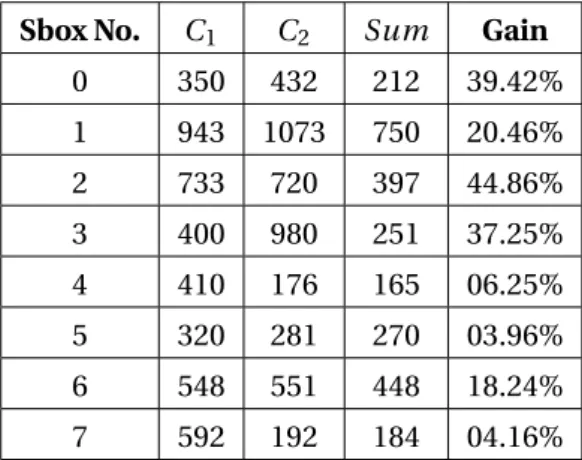
Table 5: Nombre de traces nécessaires pour attaquer C1, C2et la combinaison des deux.
Sbox No. C1 C2 Sum Gain 0 350 432 212 39.42% 1 943 1073 750 20.46% 2 733 720 397 44.86% 3 400 980 251 37.25% 4 410 176 165 06.25% 5 320 281 270 03.96% 6 548 551 448 18.24% 7 592 192 184 04.16%
résultats sont présentés dans le tableau5et on peut observer que l’attaque par combinaison est meilleure que l’attaque en utilisant une seule trace; le gain varie de 3.96 à 44.86%.
Conclusions
Pour résumer, nous avons développé les points suivants dans cette thèse:
• J’ai montré que la logique “Dual Rail” a une excellente résistance contre les attaques par injection de fautes,
• J’ai proposé la logique “Dual rail” sans EPE, et BCDL comme une contre mesure DPL résistant EPE,
• J’ai proposé une architecture BCDL résistante à un déséquilibre de routage, avec un faible “fan-out”.
• J’ai aussi proposé comme contre mesure aux canaux auxiliaire, une architecture "Un-rolling"
• J’ai montré que le modèle stochastique sont des outils appropriés pour l’évaluation des architectures DPL.
• J’ai proposé une méthodologie pour combiner les mesures pour accélérer les attaques par canaux auxiliaires.
Comme perspectives de ces travaux, je propose une implémentation masquée de la BCDL en utilisant plusieurs bits de masque et qui basculerait entre deux réseaux. La carac-térisation des fuites durant les phases de conception est aussi un sujet qui mériterait d’être
approfondi. On pourrait utiliser dans ce contexte une modélisation multivariée stochas-tique.
Introduction
1.1 Motivation
Field programmable gate arrays (FPGA) which have significantly evolved during recent years, are capable of implementing complex system on chip (SoC) and providing high perfor-mance. Therefore FPGA are finding wide application in complex systems. The main advan-tages of FPGA over application specific integrated circuits (ASIC) are its reconfigurability, shorter time to market and frequent design updates. They are also economical compared to ASIC when deployed in low volume. Owing to these advantages, FPGA find application in digital signal processing, software-defined radio, medical imaging, computer vision, speech recognition and cryptography. FPGA are also used even in sensitive domains like defence and space. For security needs, SoC embeds cryptographic cores (crypto-cores) to encrypt all the communication in a SoC. Also in applications like network routers, FPGA are deployed to encrypt the data packets before sending them at a high speed. These communications are as secure as the crypto-cores which are generally computationally secure however physical implementations can leak sensitive information.
Several successful attacks against such cores have been put forward which target their physical implementation. The first physical attack to be published was the “timing attack”, presented by Kocher et al. in 1996 [1]. In this attack, an adversary is able to recover a secret key employed in a signature algorithm by spying on the execution time of various operations. This attack is an example of “side-channel attack” as it is completely passive: the attacked system is not aware of the threat. Other side-channel attacks spying on tar-get properties like power consumption and electromagnetic radiation have been reported since then [2,3], and their study has mobilized many researchers. Such attacks unfold in two stages: side-channel information collection and side-channel analysis (often abridged
SCA). Side-channel collection is a “metrology” step, whereas SCA requires sophisticated the-oretical tools to be efficient. Both aspects are advancing rapidly, as attested for instance by the “DPA contest” competitions [4]. Another class of physical attacks known as active or “fault attack” (FA) works by altering the functional behavior of the attacked device by per-turbations [5,6].
Since then many countermeasures have been devised to secure physical implementa-tion of crypto-cores. The primary aim of these countermeasures is to remove any depen-dency between internal operations of a crypto-core and the corresponding leakages. Most, if not all, countermeasures use redundancy to strengthen the crypto-core against SCA and FA. These countermeasures can be widely classified into two categories:
1. information masking [7, Chap. 9], which aims at randomizing the side-channel leak-age, and
2. information hiding [7, Chap. 7], which aims at hiding the secret information present in the side-channel.
Information masking based countermeasures use a randomly generated value called “mask” in a way that side-channel leakage is corresponding to the mask without affecting the value of the output ciphertext. Proper implementation of masking countermeasures is secure against first order SCA but higher-order SCA might be successful. Information hid-ing countermeasures, as the name suggest, try to hide the information from an attacker. Resistance of these countermeasures against FA has not been studied deeply.
In the presented work, focus is laid upon the study of information hiding countermea-sures which can be implemented on commercial FPGA. Our objective consists in study-ing the rationale of these countermeasures, their efficient FPGA implementation along with their security analysis against state of the art SCA and FA. The information hiding counter-measures which I focus on are loop unrolling of crypto-cores and dual-rail precharge logic
(DPL).
1.2 Organization
This thesis is organised as follows:
Chapter2gives a general background about cryptography, common cryptographic al-gorithms, physical attacks on cryptography and corresponding countermeasures. A short introduction to FPGA is also given.
Chapter3is divided into two parts. The first part discusses improving the robustness of crypto-cores by proper implementation of some algorithm components. Different im-plementation of a non-linear component (substitution box) of an AES crypto-processor are compared in terms of implementation cost and security evaluation against SCA and FA. In the second part, I propose an information hiding countermeasure called “Unrolling” which consists of loop unrolling of the cryptographic algorithm. This countermeasure has been implemented on a DES crypto-processor and tested on a FPGA as well as an ASIC. Detailed security evaluation of the ASIC implementation supports this countermeasure.
In Chapter 4, another information hiding countermeasure called dual-rail precharge logic (DPL) is studied. I first present the basic principles of DPL in detail and FPGA im-plementation of the wave dynamic differential logic (WDDL) [8]: one of the first DPL coun-termeasure well suited for FPGA. Then, I analyze WDDL against attacks with special focus on FA. This is followed by a complete state of the art of DPL countermeasures for FPGA which were proposed as an improvement over WDDL. Finally, I extend findings regarding fault resistance of WDDL to other DPL in general.
Chapter5presents two novel DPL countermeasures for FPGA. DPL w/o EPE (early prop-agation effect) counters a common DPL flaw of EPE by modifying the truth table of the basic gates which can be implemented in FPGA by forcing pre-computed LUT mask. The second countermeasure is balanced-cell based dual-rail logic (BCDL). It features a global synchro-nization signal PRE for countering EPE and enables to use embedded memories in FPGA. I show efficient implementation of the two DPL countermeasures on FPGA. Proper evalua-tion of these countermeasures is provided to demonstrate their strength in terms of security gain.
In Chapter6, I propose two evaluation techniques. The first evaluation technique ap-plies only to DPL implementations where I use profiled attacks like templates and higher order stochastic models for precise evaluation. The interest of using these attacks are two fold: precise estimation of leakage and pin-pointing the source of leakage. These meth-ods are tested in a simulated environment and on real traces from FPGA implementation of DPL w/o EPE. The second evaluation technique is called combined attacks. The principle of this attack is that multiple measurements of the same activity can be combined to accel-erate the attacks on a given implementation. Theoretical background along with practical application is given.
1.3 Contributions
The main contributions of this work are:
1. Comparison of various s-box architectures in an AES co-processor against setup time violation faults [A].
2. Analysis of WDDL countermeasure against setup time violation faults [B] followed by extension of results to DPL in general [C,D].
3. Proposing unrolling of cryptographic algorithms as a side channel countermeasure [E].
4. A novel DPL countermeasure (DPL w/o EPE) for FPGA capable to countering the EPE flaw [F].
5. A novel DPL countermeasure (BCDL)[G] with its efficient implementation on FPGA to counter EPE and technological imbalance [H].
6. Application of advanced evaluation tools like templates and higher order stochastic models for efficient DPL evaluation and implementation [I].
7. A technique to combine multiple measurements of the same activity to accelerate side channel attacks [J].
General Background
“Cryptology” stems from the Greek root crypto that means “hiding”. Cryptology includes two branches “cryptography” and “cryptanalysis”. Cryptography is the study of techniques to protect sensitive information from third parties by encoding it into an unreadable form. It is used to transform legible information (plaintext) into a protected form (ciphertext) with the help of secret information (key). According to Kerckhoffs’s principle, any information related to cryptographic system can be public except the key. Cryptanalysis comprise of all the methods which can be deployed to obtain the plaintext or the decryption function in a cryptosystem by eavesdropping into the insecure channel.
Cryptography was used throughout the history. Secrecy was used by individuals and governments to hide the true intentions and gain competitive advantage. The first recorded use of cryptography in writing dates back to 2000 BC when the Egyptian used nonstandard hieroglyphs in an inscription. Hieroglyphics were used mainly in the tombs of the pharaohs to tell the story of the life of the deceased, however the intentions was not to hide informa-tion. Around 400 BC, the second clue about using cryptography was discovered in Greece. Greeks used scytale code, to encrypt information, and that is to write a message on a sheet of papyrus, which was wrapped around a rod. The only way to read it to find a rod with exact dimensions as the source. Julius Caesar used shifting the letters of the alphabet for military purposes.
In the twentieth century, cryptography played a crucial role in the outcome of both world wars. It was widely used in communication systems related to military, diplomatic service and government in general. The overall goal was primarily to protect state secrets and strategies. Indeed, during the World War II, modern cryptographic engines were de-signed for tactical communications, which greatly improved technology promotion, such as the telegraph and radio communications. For example, the so-called rotary encoder, is
an electro-mechanical device that converts the angular position or motion of a shaft or axle to an analog or digital code. It was a huge breakthrough in military cryptography. This machine was considered unbreakable for a significant period of time. Moreover, it was the source of the most famous cipher machine in history, designed by the German engi-neer Arthur Scherbius called Enigma machine, which consists of three rotors. Although the Enigma machine was technically difficult for the time, the system was broken by the Polish Cipher Bureau. Broken code was the shared with the British military intelligence, which was used against an attack strategy in Germany and military traffic. It has played a very impor-tant role during World War II, and often reported in the literature. After the war, details of Enigma machines are published in [9].
2.1 Modern Cryptography
From the birth of computers and new communications systems in the 1960s, the ability to encrypt using advanced engines expanded exponentially. Computers have provided sys-tem designers with an excellent opportunity to improve cryptography. Moreover, there was an increased need for cryptography in the sector of computer technology to provide digital information and ensuring security. In the literature, this new era of cryptography is often referred to as Modern Cryptography. Modern cryptography is a mixture of security engi-neering and mathematics to form the basis of security.
The most famous project in cryptography was developed by IBM and called Lucifer. Lu-cifer was based on complex mathematical functions, which were subsequently adopted and modified by U.S. National Security Agency (NSA), to become the U.S. Data Encryption Stan-dard (DES), called secret-key cryptography (SKC). SKC uses one key for encryption and de-cryption. Thereafter, data encryption standard (DES [10]) was formally adopted by the U.S. Federal government as a standard in 1977. DES is still used for securing e-commerce ap-plications in many financial institutions. Diffie and Hellman also made a major contribu-tion to cryptography in 1976. Their work has presented the basic concepts of Public-key
cryptography (PKC [11]). PKC uses one key for encryption and another for decryption, and
also provided an innovative technique for key exchange. The idea behind this technique was based on unresolved discrete logarithm problem. Even if the authors did not provide a practical implementation of the proposed encryption scheme, as it was impossible to real-ize at that time, the idea was clear, and it was a source of extensive research in cryptography community.
In 1978, the three cryptographers Rivest, Shamir and Adleman developed the first prac-tical public-key encryption and signature scheme, called RSA [12]. Difficulty of factoring the large numbers was a major mathematical problem, which was used in RSA scheme. Since then, extensive research in both the private key and public key encryption is being con-ducted.
The so-called 3-DES was the successor to DES. This new algorithm is basically starting from DES, but uses three secret keys for encryption and decryption. Since DES was broken in early 1990s 3-DES was put in place. 3-DES was considered safe and accepted by many fi-nancial institutions around the world. In the late 1990s, NIST decided the new standard, Ad-vanced Encryption Standard (AES [13]). AES is an efficient secret-key algorithm with more complex mathematical functions, providing a higher level of security. AES has a lot of op-tions, depending on the key-space, which is the range of values that can be used as key. The larger the key space, more available options may be used to represent the different keys, and the more difficult for attackers to find the secret key.
As for public-key encryption, the existing mechanisms are still evolving. In fact, an-other class of powerful and practical public-key scheme, also based on the discrete loga-rithm problem, was developed in 1985, by El-Gamal. In principle, one of the most inter-esting application of the public key cryptography is the Digital Signature Algorithm (DSA). In 1991, the first international standard for digital signatures based on the RSA public key scheme, was formally adopted. In 1994, the new standard, based on the ElGamal public key system was adopted by the U.S. Government. Successor to such plans is elliptic curve DSA (ECDSA). In fact, Elliptic Curve Cryptography (ECC [14]) provides many features like RSA, such as encryption, digital signatures and secure key distribution.
Another type of encryption introduced recently is one-way cryptography. The algo-rithms are based on one side functions known as hash function. They are mainly used to identify the various parties in communication and find wide application in digital signa-tures. Following provides a detailed outlook on SKC and PKC.
2.2 Symmetric Key Cryptography
Secret-key cryptography is where a single key is shared between the transmitter and re-ceiver. This means that the same key is used for encryption and decryption. For this reason, secret-key cryptography is also called symmetric key cryptography. Obviously, the major dif-ficulty of symmetric encryption is the distribution of the secret key that must still be secret,
known only by the sender and receiver. Secret key cryptography is further classified into
stream ciphers and block cipher.
2.2.0.1 Stream Ciphers
Stream ciphers are an important class of encryption algorithms. It is a symmetric key cipher where message (plaintext) is combined with a pseudorandom keystream. Some ciphers use what is known as the key-stream generator, leading to a bit stream which is XORed1with the plaintext to produce a ciphertext [15]. In the open literature, there are two common stream ciphers used in practice:
• Self-synchronizing stream ciphers that computes a key-stream according to few pre-vious ciphertexts. A common problem with encryption is the propagation of errors. Indeed, a slight modification in transmission will result in n bit-change at reception. • Synchronous stream ciphers produces the key stream in a manner independent of the
message. However, the same function key stream generation is used for transmission and reception. Such stream ciphers are not affected by transmission errors.
Evaluation of the effectiveness of stream ciphers is done on three grounds: First, no repeating patterns within the main-stream values should exist at least for long periods, sec-ond, the key-stream cannot be linearly related to the key and the third, key-stream should be statistically unpredictable. From the perspective of design, stream ciphers are suitable for hardware implementations, and we can expect an increasing use of such ciphers in the coming years.
2.2.0.2 Block Ciphers
Basically, block cipher algorithms are used for encryption and decryption. They aim to di-vide a message into blocks of bits, which are then processed by several mathematical func-tions such as substitution and transposition. In fact, block-cipher processes the plaintext into blocks of bits relatively large (i.e. 64 bits, 128 bits ...). Same function is applied to en-crypt successive blocks, thus block ciphers are memory-less. In contrast, stream ciphers, when using the encryption function may vary according to the plaintext, which require a large memory. Block ciphers are strong and difficult to break mathematically. Block ciphers are used in five common modes of operations.
• Electronic Code Book (ECB) mode The same block of ciphertext is always generated for a given block of message and key. ECB mode is often used for small block sizes, such as encryption and protection of encryption keys.
• Cipher Block Chaining (CBC) mode Each block of plaintext is XORed with the pre-vious encrypted block before being encrypted. In this way, each encrypted block depends on all the blocks processed up to that point. Also, to make each message unique, an initialization vector IV is used in the first block.
• Cipher Feedback (CFB) mode The data is encrypted in blocks smaller than the size of the initial block. CFB mode works like the self-synchronizing stream cipher.
• Output Feedback (OFB) mode An internal feedback mechanism is used to prevent the same plaintext block to generate the same block of ciphertext. This method is technically similar to synchronous stream ciphers.
• Counter Mode generates the next keystream block by encrypting successive values of a "counter". The counter can be any function which produces a sequence which is guaranteed not to repeat for a long time.
Typically, each mode is designed to manage how a block cipher will work. The choice of a mode is essentially based on security requirements.
2.2.1 Data Encryption Standard
As presented in the FIPS standard, DES is designed to cipher and decipher blocks of data. The messaage has a block size of 64 bits while the key is 56 bits. Deciphering is done with the same key as for ciphering, but in reverse order of the ciphering process. Ciphering a block starts with an initial permutation IP followed by complex key-dependent computation and finally a permutation which is the inverse of the initial permutation I P−1. Figure2.1shows the DES algorithms. The key-dependent computation can be defined by a function f, called the cipher function, and a function KS, called the key schedule [10].
Eavesdroppers of the cipher know the algorithm but do not have the correct key which deprive them from extracting the original data. However, anyone who does have the key and the algorithm can easily decipher the original data. A standard algorithm based on a secure key thus provides a basis for exchanging encrypted computer data by issuing the secret key for authorized users. A wrong key causes the ciphertext that is produced for any given set of inputs to be different. But with the increase of the computation speed in new computers,
R15 L15 R15 L16 R0 L0 S0 S7 S6 S5 S S3 S2 S1 R1 L1 IP IP Key Key16 2 32 32 64 64 48 48 48 f f Key1 f 48 32 32 32 P E Key 32 32 32 32 48 6 4 6 4 6 4 6 4 6 4 6 4 6 4 4 6 4 Plaintext Ciphertext −1
Figure 2.1: Data Encryption Standard
brute force attack have become possible (which means a trial of all possible values of the key). In fact, in June 1997 the DES was cracked by using a network of normal computers and it took 23 hours and 15 minutes [16]. Thus, an urgent need for a more robust encryption algorithm was felt. The first idea was to use 3-DES which consists in using a call of DE S, then DE S−1, and finally DE S.
2.2.2 Advanced Encryption Standard
In 2000, NIST chose the ‘‘Rijndael” algorithm as the algorithm for Advanced Encryption Standard (AES) [13]. AES is an encryption algorithm invented by Joan Daemen and Vincent Rijmen which works on block of 128 bits, and a key of variable length. The length 128, 192, 256 allows a trade off between security and efficiency (speed, computation complexity, im-plementation cost). AES is an iterative algorithm where the number of rounds depend on the length of the key. There are 10, 12 or 14 rounds for a 128, 192 or 256 bits of key respec-tively.
Furthermore, AES encryption and decryption are based on four different transforma-tions that are performed repeatedly in a certain sequence. Each transformation maps a 128-bit input state addressed byte-wise into a 128-bit output state. The set of transforma-tions which is repeated every time is called a round. The rounds are slightly different for encryption and decryption. These transformations are described in the pseudo-code given below. Round=0; AddRoundKey(State,RoundKey); Round++; while i<10 { Round(State,RoundKey) { SubBytes(State); ShiftRows(State); MixColumns(State); AddRoundKey(State,RoundKey); }; Round++; }; FinalRound(State,RoundKey) { SubBytes(State); ShiftRows(State); AddRoundKey(State,RoundKey); };
The 128-bit data block is treated as a 4×4 array of bytes called the state matrix. The algo-rithm consists of an initial data/key addition,10 full rounds for a 128 bit key (12/14 rounds for 192/256 bits of key). The last round is slightly different from the other rounds. A dedi-cated key scheduling process is used to generate all the round keys from the input key. Each sub-key is also treated as a 4 × 4 array of bytes. A full Rijndael round involves four steps:
1. a non-linear substitution that is applied on each byte of the state matrix: “SubBytes”. 2. A circular bytes permutation within the same line: “ShiftRows”.
3. A multiplication in GF (28) for each column: “MixColumns”. 4. A simple XOR with the output of the key register: “AddRoundKey”.
SubBytes Transformation
The s-box is an invertible substitution table which is constructed by a composition of two transformations. First, each byte Ai , j is replaced by its reciprocal in GF (28) polynomial
(ex-cept 0, which has no reciprocal, is replaced by itself ) followed by an affine transformation. The s-box is usually implemented as a look-up table consisting of 256 entries, each entry is 8 bits wide, but it also can be computed in composite fields.
ShiftRows Transformation
Next comes the ShiftRows transformation, each row in a 4×4 array of bytes of data is shifted 0, 1, 2 or 3 bytes to the left in a round fashion, producing a new 4 × 4 array of bytes.
MixColumns Transformation
The MixColumns transformation, operates on each column individually where each byte is mapped into a new value that is a function of all four bytes in the column. The transfor-mation can be defined as a matrix multiplication on the state. Each column is treated as a polynomial over GF (28) and is then multiplied modulo x4+ 1 with a fixed polynomial a(x):
a(x) = (0x03)x3+ (0x01)x2+ (0x02)x + (0x02)
AddRoundKey Transformation
The final transformation is AddRoundKey, it is a bit-wise XOR of the round data with the corresponding round key for the current round.
The Key Schedule
Each round accepts a round key derived from the initial secret key by means of the Key Schedule process.
• ”Rotword” operation takes a 32-bit word and rotates it by eight bits to the left. • ”Subword” operation uses s-box table to replace each byte of the columns. • ”Rcon” is a table of constants depending on the round number.
More precisely, if k0is the secret key and kiis the it hround key, then Key Schedule com-putes ki= K Si(ki −1) as a function of the previous round key. The functions K Sithemselves
depend on the round and on the size of the key. However, the K Si do not differ much from
each other, and for a key size of 128 bits they are all identical.
2.3 Public-Key Cryptography
Symmetric ciphers are computationally strong but key management is an important issue. The secret key needs to be securely exchanged and the encryption of the secret key is not an
option, since it would represent the same problem again and again. If the key gets leaked, then it should be revoked and a new one should be shared. In addition to this, each different secure link requires its own key: every pair of users should be assigned a unique key, known only to the authorized owners, which increases the overall number of keys exponentially with additional users. Even if the key is shared within a single group of people, there would be no way to identify correctly the sender within the group, or have a subset of authorized receivers.
Public-key (asymmetric) crypto-systems were proposed to address such issues. Each user has a pair of keys: a secret key (the private key) and a public key. It is easy to compute the public key from the private key, but the inverse is computationally infeasible. Each user has a public key which is shared with other users. Anyone can use the public key to encrypt the message but it can be decrypted only by one who posses the corresponding private key. This scheme provides some very important properties for secure communications:
• Confidentiality: It is the guarantee that the message will not be read by an unautho-rized receiver; it can be achieved by encrypting the message with the public key of the receiver.
• Authentication : It is the proof of the sender’s identity, certifying that the sender of the message is actually the one who claims to be, by using one’s secret key to encrypt. • Non-repudiation: It is strictly related to the previous concept and means that the
sender can not deny having sent the message.
• Integrity : It guarantees that the message was not modified or tampered with, and it is exactly the message that was transmitted at the source.
2.3.1 RSA
The most common public-key crypto system is RSA [12], based on modular exponentiation in finite ringZn. Encryption is computed by exponentiating the message with the public key,
decryption is computed again by exponentiation with the other exponent using a secret key. Security of RSA is ensured by the problem of factoring the product of two large primes. 2.3.2 Elliptic Curve Cryptography
Recently public key algorithms have started using elliptic curves [17]. In contrast to RSA, computations take place in a finite additive group. An elliptic curve E over field K is defined