To cite this version:
Goiffon, Vincent and Corbière, Franck and Rolando, Sébastien and
Estribeau, Magali and Magnan, Pierre and Avon, Barbara and Baer, Jérémy and Gaillardin,
Marc and Paillet, Philippe and Girard, Sylvain and Molina, Romain and Chabane, Aziouz
and Cervantes, Paola and Marcandella, Claude Toward Multi-MGy / Grad Radiation
Hardened CMOS Image sensors for Nuclear Applications. (2015) In: International Image
Sensor Workshop (IISW 2015), 8 June 2015 - 11 June 2015 (Vaals, Netherlands).
O
pen
A
rchive
T
OULOUSE
A
rchive
O
uverte (
OATAO
)
OATAO is an open access repository that collects the work of Toulouse researchers and
makes it freely available over the web where possible.
This is an author-deposited version published in:
http://oatao.univ-toulouse.fr/
Eprints ID: 15773
Any correspondence concerning this service should be sent to the repository
administrator:
[email protected]
I. INTRODUCTION
HERE is a fast growing interest in the development of compact radiation hard imaging systems based on solid state image sensors that are able to provide images after the absorption of extreme radiation doses (above 1 MGy of Total Ionizing Dose (TID), i.e. 100 Mrad). This is especially true for nuclear applications[1] such as monitoring and remote handling in highly radioactive areas of nuclear facilities (e.g. nuclear power plants, nuclear waste repository, next generation particle physics facilities such as the International Thermonuclear Experimental Reactor (ITER)) but also for decommissioning nuclear facilities or for mobile rescue robots dedicated to deal with nuclear incidents.
The radiation hardness of Radiation-Hardened-By-Design (RHBD) Active Pixel Sensors (APS) has been explored and sometimes demonstrated (on technologies now obsolete) up to several hundreds of kGy (several tens of Mrad) [2]–[5]. More recently, the radiation hardness of RHBD CMOS Image Sensors (CIS) has been explored up to a few tens of kGy (i.e. a few Mrad) [6]–[8] and some dark current measurements have been reported on a RHBD APS (not based on a CIS process) for electron microscopy up to 1 MGy (100 Mrad)[9]. However, an image captured with a solid state image sensor exposed to 1 MGy(SiO2) or more has never been reported and the
radiation hardness of a modern CIS technology in the MGy range has never been studied.
The aim of this work is to design and characterize a fully radiation-hardened-by-design CIS in the MGy range to demonstrate that an imaging system which can withstand MGy dose levels is feasible. A new RHBD photodiode layout is proposed and its performances are compared to the most promising existing solutions.
II. PHOTODIODE DESIGN SELECTION
The main degradation mechanism in Pinned PhotoDiode (PPD) and 3T CIS pixels at high TID is the
V. Goiffon, F. Corbière, S. Rolando, M. Estribeau, P. Magnan, B. Avon, J. Baer, R. Molina, A. Chabane and P. Cervantes are with ISAE-SUPAERO, Université de Toulouse, 10 avenue Edouard Belin, 31055 Toulouse, France, (e-mail: [email protected]).
M. Gaillardin, P. Paillet and C. Marcandella are with CEA, DAM, DIF, F-91297 Arpajon, France.
S. Girard is with Université de Saint-Etienne, Laboratoire Hubert Curien, UMR-CNRS 5516, 42000 Saint-Etienne, France
effect of the radiation induced positive charge trapping (Fig.1) in the Shallow Trench Isolation (STI), the Transfer Gate (TG) spacer and the Pre-Metal-Dielectric (PMD) that leads to the depletion and the inversion of the P- doped layers (including the pinning layer).
In PPD pixels, it induces huge image lag followed by a disappearing of the pinning layer an no existing RHBD technique can mitigate that [10]. In 3T pixels it leads to a short-circuit between the photodiode and the surrounding N regions and to a large drop of CVF[8] that can be both mitigated using RHBD techniques. For these reasons, PPDs were excluded for this study (including hole channel PPDs that are also likely to suffer from important image lag at high TID because of the PMD/spacer trapped charge) and conventional photodiodes hardened-by-design were selected.
The two most promising solutions identified in [8] were chosen: the gated [2], [3], [8], [11], [12] and the P+ surround [8] photodiodes (Fig.2). In classical gated photodiode designs, the N implant is either self-aligned on the gate edge (by using a self-aligned N+ implant [2], [3], [11]) or voluntarily drawn to cover only the P
T
Toward Multi-MGy / Grad Radiation
Hardened CMOS Image Sensors
for Nuclear Applications
Vincent Goiffon, Franck Corbière, Sébastien Rolando, Magali Estribeau, Pierre Magnan,
Barbara Avon, Jérémy Baer, Marc Gaillardin, Philippe Paillet, Sylvain Girard, Romain Molina,
Aziouz Chabane, Paloa Cervantes and Claude Marcandella
Fig. 1. Radiation induced degradation mechanisms in Pinned Photodiode based pixels and in conventional photodiode (3T) based pixels at high TID (>20kGy/>2Mrad). The “+” and “-” signs represent trapped positive charges and interface states respectively. Bold “+” and “-” signs represent defects with major influences.
region[8], [12]. It means that classical gated photodiode designs are never meant to cover the N depleted region. It has two major consequences: 1) the N depleted region is in contact with the PMD interface where a higher interface state density (Nit) than at the gate oxide interface
is expected; 2) at the optimum voltage (P region in accumulation) the depleted region is pinched between the highly doped N region and the accumulated P region, which leads to high Electric Field Enhancement (EFE) of the dark current.
To mitigate this gated photodiode design limitations, a new design is proposed and tested here: the Gate Overlap design which corresponds to a gated photodiode layout where the gate completely covers both N and P depleted regions. By doing so, only the gate oxide is in contact with the PN-junction and the electric field enhancement at optimum gate voltage should be slightly reduced (Fig.2).
III. EXPERIMENTAL DETAILS
The studied CIS is constituted by a 128x128-10µm-pitch-3T-pixel-array and it has been fully hardened against TID effects (full Enclosed Layout Transistor (ELT) design including all NMOSTs and all PMOSTs). The pixel array is divided in 4 pixel subarrays (as
illustrated in Fig. 3), each one with a particular photodiode design (but with the same in-pixel MOSFETs): the Standard photodiode design, the P+ surround, the proposed Gate Overlap and the Classical Gated Self-Aligned. Before irradiation, the Charge-to-Voltage conversion Factor (CVF) values were about 4.8µV/e- for the Standard design and 4.4 µV/e- for the other pixel types.
The selected manufacturing process is a commercially available 180 nm CIS process. Irradiations were performed with an ARACOR semiconductor 10keV X-ray irradiator at room temperature with worst case bias conditions (i.e. CIS powered and operated) applied during exposure (with no lid and no cover glass between the X-ray beam and the integrated circuit). The gates used to harden the Gated Self Aligned and Gated Overlap pixels were biased to 3.3V during irradiation. This gate bias condition represents an unrealistic worst case (high positive voltage) and possibly lower degradation could be obtained by applying a voltage more representative of real operation conditions (0V or slightly negative voltage) on the gate during exposure.
There was an issue during the manufacturing of this
Fig. 2: Cross sectional views of the studied photodiode layouts. The optimum gate bias is a slightly negative voltage to approach the accumulation regime in the P-doped gate region. In the gated layouts (c and d) a P+ ring is used as in [11] to stop the depletion region extension but it is not really useful here because the optimum gate regime is the accumulation (as shown in Fig.4).
Before irradiation After 4MGy/400Mrad(SiO2)
Fig. 3: Raw images captured before and after 4 MGy(SiO2) (400 Mrad(SiO2)) of TID. The pixel array is divided in 4 pixel subarrays, from top-left to bottom-right: Standard photodiode design, P+ surround, Proposed Gate Overlap and Classical Gated Self-Aligned.
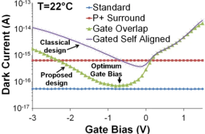
Fig. 4: Dark Current as a function of Gate Bias before irradiation. The proposed design reaches the performances of the standard diode before irradiation for a gate bias of –0.7V whereas the classical design exhibits a much higher dark current because of the Electric Field Enhancement (EFE).
Fig. 5: Absolute External Quantum Efficiency (EQE) (=QExFF) before irradiation. The use of a gate in the radiation hardened pixels lead to an acceptable EQE reduction at short wavelengths. The difference in EQE between the two gated designs is not significant.
test chip: the channel doping profile of in-pixel MOSFETs has not been properly implanted. Because of that, the threshold voltage of in-pixel MOSFET is much higher than the value targeted during the design phase leading to a Maximum Output Voltage Swing(MOVS) much lower than expected (about 600-700mV instead of more than 1V). The main cause of this limited MOVS is not due to the RHBD techniques and this issue should be solved on the next test chip.
IV. RESULTS
Before irradiation, the proposed Gate Overlap layout exhibits limited performance degradation compared to the standard layout (Fig. 3, 4 and 5). After 4 MGy(SiO2) (i.e. 400 Mrad), the two gated photodiode designs are still able to provide useful images (Fig.3), validating the functionality of the radiation hardened sensor in the MGy range. Similar results have been obtained after 10 MGy(SiO2)/1 Grad(SiO2) of absorbed TID (picture not shown here).
Contrary to what is usually observed at lower TID, it appears that GO2 ELT PMOSFETs suffer from large threshold voltage Vth shifts (due to radiation induced positive trapped charge in the gate oxide) when the MGy range is approached whereas GO2 ELT NMOSTs are
weekly impacted (Fig.6). There is neither data nor study of ELT PMOST irradiated in the MGy range in literature. However, this unexpected dissymmetry agrees well with the few published results on non-ELT irradiated GO2 PMOST in the MGy range [13]. The physical explanation of this dissymmetry between N and PMOST gate oxide is under investigation. To keep good speed performance, the voltage bias of the PMOST current source has been shifted to compensate the Vth shift at high TID leading to a limited decrease of the maximum output voltage swing.
The whole sensitivity (EQE×CVF×Readout Gain) remains acceptable (Fig.7 and 8) on the gated designs for the targeted applications after 4 MGy(SiO2) (less than 25% drop) whereas the standard diode layout becomes completely insensitive to light between 10 and 100kGy (1 and 10 Mrad). This drop is due to the inversion of the surrounding P doped region leading to a short-circuit between the standard photodiodes.
The remaining sensitivity degradation on the gated photodiode pixels is due to a combination of surface recombination intensification and a readout gain variation
Fig. 6: Radiation Induced Threshold Voltage Shift (∆Vth)
measured on individual GO2 ELT N and P MOSFETs. GO2 stands for double gate oxide (i.e. 3.3V MOSFETs).
Fig. 7: Normalized sensitivity with TID at 650 nm. The Gated SA design sensitivity is not shown because it has the same behavior as the Gate Overlap design.
Fig. 8: Electro-optical transfer function before irradiation and after 4MGy(SiO2). The overall performances are still reasonable
for the gated designs after 4MGy whereas the standard design is no longer sensitive to illumination.
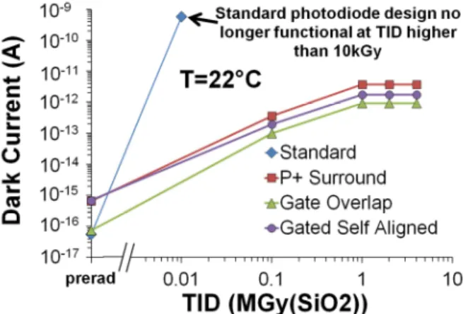
Fig. 9: Dark Current versus Total Ionizing Dose (TID). At 0.1 MGy the standard layout is no longer functional (all the photodiodes are short-circuited through the inversion layer) and the dark current cannot be evaluated. The proposed gate overlap design still brings an appreciable improvement after the maximum TID. As reported below 1MGy in [9] the dark current saturates at high TID (most likely because of the saturation of the interface state density in the MGy range).
and by the change of bias voltage). Dark current values (Fig. 9) are skyrocketing for the standard design whereas the RHBD photodiodes are able to contain the unavoidable dark current rise with TID (best results are obtained with the Gate Overlap design).
V. CONCLUSIONS AND PERSPECTIVES
This work demonstrates that CIS can be radiation hardened to operate in the MGy range (> 100Mrad) and even beyond (images at 10MGy/1Grad have also been obtained). The proposed improved gated photodiode design appears to be more efficient at mitigating TID effects than other classical radiation hardened designs. The main weakness of this first test vehicle is the large PMOSFET degradation still under investigation that will be mitigated in the next test chip.
REFERENCES
[1] J. W. Cho, Y. S. Choi, and K. M. Jeong,
“Monitoring performance of the cameras under the high dose-rate gamma ray environments,” Health
Phys., vol. 106, no. 5 Suppl 2, pp. S47–58, May
2014.
[2] B. R. Hancock, T. J. Cunningham, K. P. McCarty, G. Yang, C. J. Wrigley, P. G. Ringold, R. C. Stirbl, and B. Pain, “Multi-megarad (Si) radiation-tolerant integrated CMOS imager,” in Proc. SPIE, 2001, vol. 4306, pp. 147–155.
[3] B. Pain, B. R. Hancock, T. J. Cunningham, S. Seshadri, C. Sun, P. Pedadda, C. J. Wrigley, and R. C. Stirbl, “Hardening CMOS imagers: radhard-by-design or radhard-by-foundry,” in Proc. SPIE, 2004, vol. 5167, pp. 101–110.
[4] E.-S. Eid, T. Y. Chan, E. R. Fossum, R. H. Tsai, R. Spagnuolo, J. Deily, W. B. Byers, and J. C. Peden, “Design and characterization of ionizing radiation-tolerant CMOS APS image sensors up to 30 Mrd (Si) total dose,” IEEE Trans Nucl Sci, vol. 48, no. 6, pp. 1796–1806, Dec. 2001.
[5] J. Bogaerts, B. Dierickx, G. Meynants, and D. Uwaerts, “Total dose and displacement damage effects in a radiation-hardened CMOS APS,” IEEE
Trans Electron Devices, vol. 50, no. 1, pp. 84–90,
Jan. 2003.
[6] M. Innocent, “A radiation tolerant 4T pixel for space applications,” in Proc. IISW, 2009. [7] V. Goiffon, M. Estribeau, O. Marcelot, P.
Cervantes, P. Magnan, M. Gaillardin, C. Virmontois, P. Martin-Gonthier, R. Molina, F. Corbiere, S. Girard, P. Paillet, and C. Marcandella, “Radiation Effects in Pinned Photodiode CMOS Image Sensors: Pixel Performance Degradation Due to Total Ionizing Dose,” IEEE Trans Nucl Sci, vol. 59, no. 6, pp. 2878–2887, Dec. 2012.
[8] V. Goiffon, P. Cervantes, C. Virmontois, F. Corbiere, P. Magnan, and M. Estribeau, “Generic Radiation Hardened Photodiode Layouts for Deep Submicron CMOS Image Sensor Processes,” IEEE
Trans Nucl Sci, vol. 58, no. 6, pp. 3076–3084, Dec.
2011.
[9] D. Contarato, P. Denes, D. Doering, J. Joseph, and B. Krieger, “High Speed, Radiation Hard CMOS Pixel Sensors for Transmission Electron
Microscopy,” Phys. Procedia, vol. 37, pp. 1504– 1510, 2012.
[10] V. Goiffon, M. Estribeau, P. Cervantes, R. Molina, M. Gaillardin, and P. Magnan, “Influence of Transfer Gate Design and Bias on the Radiation Hardness of Pinned Photodiode CMOS Image Sensors,” IEEE Trans Nucl Sci, vol. 61, no. 6, Dec. 2014.
[11] W. Dulinski, A. Besson, G. Claus, Claude Colledani, G. Deptuch, M. Deveaux, G. Gaycken, D. Grandjean, A. Himmi, C. Hu, Kimmo
Jaaskeleinen, M. Szelezniak, I. Valin, and M. Winter, “Optimization of Tracking Performance of CMOS Monolithic Active Pixel Sensors,” IEEE
Trans Nucl Sci, vol. 54, no. 1, pp. 284–289, Feb.
2007.
[12] M. Battaglia, D. Contarato, P. Denes, Dionisio Doering, P. Giubilato, T. S. Kim, S. Mattiazzo, V. Radmilovic, and S. Zalusky, “A rad-hard CMOS active pixel sensor for electron microscopy,” Nucl
Instr Meth A, vol. 598, no. 2, pp. 642–649, Jan.
2009.
[13] F. Faccio and G. Cervelli, “Radiation-induced edge effects in deep submicron CMOS transistors,”
IEEE Trans Nucl Sci, vol. 52, no. 6, pp. 2413–