T
T
H
H
È
È
S
S
E
E
En vue de l'obtention du
D
D
O
O
C
C
T
T
O
O
R
R
A
A
T
T
D
D
E
E
L
L
’
’
U
U
N
N
I
I
V
V
E
E
R
R
S
S
I
I
T
T
É
É
D
D
E
E
T
T
O
O
U
U
L
L
O
O
U
U
S
S
E
E
Délivré par Université Toulouse 3 Paul Sabatier (UT3 Paul Sabatier) Discipline ou spécialité : Génie Electrique
Présentée et soutenue par Yuan ZHANG Le jeudi 4 décembre 2014
Titre :
A new flat dark discharge lamp for backlight applications based on electron– excited– phosphor luminescence
JURY
Jean-Marc Bauchire, Prof. Ray-Lee Lin, Prof. Christian Glaize, Prof.
Yann Cressault, Maître des Conférences HdR.
Ecole doctorale : ED GEET
Unité de recherche : Laboratoire plasma et conversion d’énergie Directeur(s) de Thèse : Georges ZISSIS
i
Acknowledgements
First of all, I would like to express my deepest gratitude to Professor Georges Zissis, my research supervisor, for his patient guidance, enthusiastic encouragement and useful critiques of this research work. He has deep insight into the lighting and light sources industry, and is quite sensitive to the new trends in the technology development. Every discussion with him will inspire me with many new ideas. He is always confident and optimistic in the face of difficulty. What I learn from him is not only about the knowledge but also the attitude to the future life.
I would like to thank Dr. Sounil BHOSLE for his guide and help with the vacuum system and the glass work, and Dr. Spiros Kitsinelis for his advice and assistance on the experiment and my paper work. My grateful thanks are also extended to all the teachers and technicians in our group: such as Mr. David BUSO, Mr. Laurent CANALE, Mr. Pascal DUPUIS, Mr. Manuel LOPES, Mr. Marc TERNISIEN, Mr. Cédric RENAUD, Mr. Jean-Luc, Mr. Gérald LEDRU and etc, for their kind and patient suggestions, without which I could have not complete my thesis.
My sincere appreciation goes to my dear colleagues: Lydie AREXIS BOISSON, Arezki TOUMI, Ikbal MARGHAD, Laure BARREYRE-PANDELE, Angel BARROSO, Sovannarith LENG, Alaa ALCHADDOUD, Feng TIAN, and Ahmad Nazri Dagang. Your warmheartedness and kindness support my daily life and study in France.
I wish to appreciate the help provided by Prof. M.C. Liu and and his group from Energy and Environment Research Laboratories of Industrial Technology Research Institute in Taiwan, who participated this study with great cooperation. And I would like to acknowledge the generous help from Prof. Shanduan ZHANG and other faculties and friends in Fudan University too.
I would also like to extend my thanks to all the members in laboratory Laplace and all my dear friends in France and China for their encouragement and support. It is indeed my pleasure to meet and cooperate with them.
ii
Finally, I wish to thank my parents for their support and encouragement throughout my study and life.
iii
Table of contents
Acknowledgements ...
iTable of contents...
iiiGeneral introduction ...
1CHAPTER I: ...
3Introduction- Electrical Light Sources ...
3I.1 Incandescent Lamps ... 3
I.2 Mechanism of Discharge Lamps ... 5
I.2.1 Brief history of the gas discharge research ... 5
I.2.2 Voltage- current characteristic curve of discharge lamp ... 8
I.2.3 Discharge Lamps ... 11
I.2.4. Mercury problem for discharge lamp ... 12
I.2.5 Lighting Mechanism ... 12
I.3. Solid-state Lamps (SSL) ... 14
I.3.1 LED ... 14
I.3.1 OLED ... 26
I.4 The Work of This Thesis ... 33
I.5 Summary ... 34
References ... 36
CHAPTER II: ...
41Theoretical Analysis on the FDDL ...
41II.1 Introduction ... 41
iv
II.2.1 Introduction to FDDL ... 42
II.2.2 Comparison with the similar applications ... 43
II.2.3 Characteristics of FDDL ... 45
II.3 Physics of discharge theory ... 50
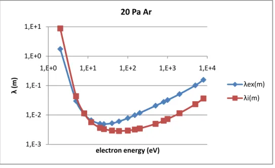
II.3.1 Mean free path ... 50
II.3.2 General diffusion ... 52
II.3.3 Townsend discharge theory ... 54
II.4 Theoretical Analysis on the FDDL ... 58
II.4.1 Ions and electrons current distribution with x position ... 58
II.4.2 Analyses by mean free path of ionization and excitation collision ... 60
II.5 Conclusion ... 66
Reference ... 67
CHAPTER III: ...
69Experiment Results on FDDL ...
69III.1 Introduction ... 69
III.2 Measurement of Basic Quality ... 69
III.2.1 Phosphor response to the laser ... 69
III.2.2 FDDL sample tests ... 72
III.3: Lamp Character at Different Pressures ... 79
III.3.1 Experiment setup ... 80
III.3.2 Neon at 0.19 mbar and 0.20 mbar ... 81
III.3.3 Neon at different pressure ... 86
III.3.4 Start voltage ... 93
III.3.5 Voltage-Current plot analysis ... 94
III.4 Commentary ... 100
III.4.1 Stability ... 100
v
III.4.3 Scanning electron microscope (SEM) analysis ... 104
III.5 Conclusion ... 107
Reference ... 108
1
General introduction
Since the first practical incandescent lamp was manufactured by Edison, electrical light sources have been developed for more than 100 years. There are three generation light sources: incandescent lamp, discharge lamp and solid state lamp. Incandescent lamps produce light by heating a filament until it glows. Discharge lamps produce light by ionizing a gas through electric discharge inside the lamp. Solid-state lamps (SSL) use a phenomenon called electroluminescence (when electrons transit between the specific energy levels of different materials in semiconductor under the external electric field, the extra energy between the band gap could be emitted by means of photons ) to convert electrical energy directly to light. The normal incandescent lamps have been banned in many countries (such as USA from 2014) due to its low luminance efficacy, since the commercial CFL and SSL products could perfectly take their place by the good lighting performance and energy saving. Although LEDs and OLEDs as typical SSL have promising future in lighting and display industry, the gas discharge lamps are still dominating the most indoor or outdoor applications nowadays. The flat dark discharge lamp (FDDL) studied in this thesis is a new kind of discharge lamp in which no mercury is used. The visible emission is coming from the phosphor instead of the discharged buffer gas, so called dark discharge lamp. It borrows the ideas from the general low pressure discharge lamp and the cathode ray tube. As a lamp its lighting mechanism is brand new compared with the traditional discharge lamps which generally work in the glow or arc discharge regime. It employs the CL phosphor (ZnS:Cu,Al+In2O3) which is widely
applied in the CRT, without which lamp could be dark. The gas pressure is about 0.2 mbar which is lower than the general low pressure mercury lamp and higher than that in the CRT or FED. This pressure can maintain high lamp voltage to accelerate electrons to excite the phosphor while the ionization of gas atoms produces electrons in the space.
Traditional discharge lamps work under glow or arc discharge regimes, while the FDDL we studied functions in the regime between Townsend discharge regimes and glow discharge region. Its gas pressure is higher than the field emission display device and its lamp voltage is higher than that of normal low pressure mercury discharge lamp or PDP. Visible radiation directly from the gas discharge is quite limited in such high E/n value (~105 Td, reduced electric field, E is electric field, n is the density of gas), but due to the high energy initial and
2
secondary electrons will contribute to the light emission. As a new candidate for the green backlight application, a better understanding needs to be explored.
The manuscript is organized in 3 chapters as follows: the first chapter presents the family of artificial electrical light sources, including incandescent lamp, discharge lamp and solid state lamp. Their history, working mechanism and development are introduced in this part. Further introduction of our lamp and some basic numerical calculation are introduced in the second
chapter, in which the excitation and ionization mean free paths are used to analyze
qualitatively the physics behind the threshold pressure for the FDDL. The lighting mechanism of FDDL is also introduced and compared with that of traditional FL, HID and CRT in this chapter. The third part shows our experiment results. The tests on the sample lamps explore some feathers of FDDL. And the experiment results of FDDL at different pressure filled with Neon and Xenon are also presented and discussed in this chapter.
This thesis work has been done in LM (Lumière et Matière) group of LAPLACE (LAboratoire PLAsma et Conversion d‘Energie) with the collaboration of Prof. M.C. Liu and his group from energy and environment research laboratories in industrial technology research institute in Taiwan.
3
CHAPTER I:
Introduction- Electrical Light Sources
Human has the inner interest for brightness. Life without light is unimaginable. In the modern times electrical light sources allow us to extend our activities, such as working, travel and entertainment, beyond the daylight hours. Factories and office buildings are designed with no possibility of ever being adequately illuminated by daylight. Worldwide communication would be impossible if half the world could not dispel the darkness by turning on the light at the flick of a switch. Electrical light sources are very important in present daily life.
The electric light sources, called lamps and used for providing illumination, can be divided into three general classes: incandescent, discharge, and solid-state lamps. Incandescent lamps produce light by heating a filament until it glows. Discharge lamps produce light by ionizing a gas through electric discharge inside the lamp. Solid-state lamps use a phenomenon called electroluminescence to convert electrical energy directly to light.
I.1 Incandescent Lamps
The incandescent lamp is one of the longest existing electro-technical products, its history comprises about 200 years. The essential start of this history is the experiment of Sir Humphrey Davy in 1802 whereby a Pt wire was heated to incandescence by the passage of current from a Voltaic pile. The first historic milestone was reached with the carbon filament lamp of Edison in 1879. And in 1912 the gas-filled tungsten filament lamp came to the world. In 1959 the halogen lamp was invented [1].
Incandescent lamp technology uses electric current to heat a coiled tungsten filament to incandescence. The glass envelope contains a mixture of nitrogen and a small amount of other inert gases such as argon. Some incandescent lamps, such as some flashlight lamps, also contain xenon. Thomas Edison‘s first carbon filament lamp had a life of about 40 hours.
4
Today, commonly available incandescent lamps have average lives of between 750 and 2000 hours. Figure 1.1 shows the construction of a typical incandescent lamp.
Incandescent lamps are strongly affected by input voltage. For example, reducing input voltage from the normal to 95% can double the life of a standard incandescent lamp, while increasing voltage to just 105% of normal can halve its life. Voltage variations also affect light output (lumens), power (watts), and efficacy (lumens per watt).
Halogen Lamps Unlike normal incandescent lamps, halogen lamps use a halogen gas fill
(typically iodine or bromine), to produce what is called a ―halogen cycle‖ inside the lamp. In the chemical formula 1.1 W is tungsten, X is halogen atom, and n is the number of atoms involved. When the temperature is low (near the bulb wall) the positive process happens (from left to right). When the temperature is high (near the filament), it goes to the opposite way (from right to left).
(𝑛𝑒𝑎𝑟 𝑡𝑒 𝑓𝑖𝑙𝑎𝑚𝑒𝑛𝑡)𝑊 + nX ↔ WXn(near the bulb) (1.1)
Halogen gas combines with the tungsten that evaporates from the lamp filament, eventually re-depositing the tungsten on the filament instead of allowing it to accumulate on the bulb wall as it does in standard incandescent lamps. The tungsten- halogen lamp has several differences from incandescent lamps: ·
1. The lamps have a longer life (2000-3500 hours). · Fig.1.1 Construction of a Incandescent lamp
5
2. The bulb wall remains cleaner, because the evaporated tungsten is constantly redeposited on the filament by the halogen cycle. This allows the lamp to maintain lumen output throughout its life.
3. The higher operating temperature of the filament improves luminous efficacy. ·
4. The lamp produces a ―whiter‖ or ―cooler‖ light, which has a higher correlated color temperature (CCT) than standard incandescent lamps. ·
5. The bulbs are more compact, offering opportunities for better optical control.
Halogen lamps are sometimes called ―quartz‖ lamps because their higher temperature requires quartz envelopes instead of the softer glass used for other incandescent lamps.
I.2 Mechanism of Discharge Lamps
The principle of a gas discharge lamp is based on the conversion of electric power into radiation by means of an electrical discharge in the gas medium in the lamp. In such lamps weakly or moderately ionized plasma is created. Plasma is an ionized gas and consists of electrons, ions, neutrals and excited particles and is on average neutral. The gas is located, in general, in a discharge tube with two electrodes [2].
I.2.1 Brief history of the gas discharge research
Gas discharge is a basic physical phenomenon in the nature. Leaving lightning alone, the first observation on man-made electric discharges can date back to 17th century, when the researcher saw the friction charged insulated conductors lose their charge. Coulomb proved experimentally in 1785 that charge leaks through air. We understand now that the cause of leakage is the non-self-sustaining discharge.
The history of gas-discharge lamps began in 1675 when French astronomer Jean-Felix Picard observed that the empty space in his mercury barometer glowed as the mercury jiggled while he was carrying the barometer [3]. Hauksbee first demonstrated a gas-discharge lamp in 1750
[4]
. He showed that an evacuated or partially evacuated glass globe, in which he placed a small amount of mercury, while charged by static electricity could produce a light bright enough to read by.
After the first battery (the voltaic pile) was developed by A. Volta in 1800, the sufficiently powerful electric batteries were developed, and this allows the discovery of arc discharge
6
which was first reported by V. V. Petrov in Russia in 1803. Several years later Humphrey Davy in Britain produced and studied the arc in air. This type of discharge became known as ‗arc‘ because its bright horizontal column between two electrodes bends up and arches the middle owing to the Archimedes‘s force. Since then, discharge light sources have been researched because they create light from electricity considerably more efficiently than incandescent light bulbs.
Fig. 1.2: Classical experimental setup for the typical gas discharge tube
The glow discharge was first discovered and studied by Faraday in thirties of 19th century. Faraday worked with tubes evacuated to a pressure about 1 Torr and applied voltage up to 1000V. In 1855, with the work of Heinrich Geissler [4], the first evacuated (~103 Pa) glass tubes (seen in Fig. 1.2) became available for scientific research and made it easy to study discharges in a more controlled environment.
Later it was discovered that the arc discharge could be optimized by using an inert gas instead of air as a medium. Therefore noble gases neon, argon, krypton or xenon was used, as well as carbon dioxide historically.
In 1889 [5], Friedrich Paschen published his work in which he investigated the minimum potential that is necessary to generate a spark in the gap between the two electrodes in gas discharge tubes. Curves of this potential as a function of pressure and the gap distance are nowadays called Paschen curves (see Fig. 1.3 (a)).
At the beginning of 1900 [6], J. S. E. Townsend proposed the theory of ionization by collision to explain the development of currents in gases, by which many phenomena in connection with the discharge through gas can be explained, including Paschen‘s observations. He introduced a coefficient α to describe the average number of electrons produced by one
R anode cathodee
e
7
electron moving through a unit length of centimeter in gas. This so-called ionization coefficient is widely used in the study of various discharge phenomena, including the work performed in this thesis. Numerous experimental results were gradually accumulated on cross sections of various electron-atom collisions, drift velocities of electrons and ions, their recombination coefficients, etc. These works built the foundations of the current reference sources, without which no research in discharge physics would be possible. The concept of plasma was first introduced by I. Langmuir and L. Tonks in 1928 [7], [8]. Langmuir also made many important contributions to the physics of gas discharge, including probe techniques [9] of plasma diagnostics.
Fig. 1.3: (a) The Paschen curves for different gases [10], the minimum in the curve is called Stolevtov‘s point; (b) the dependence of α/p on the reduced electric field E/p for various gases [11] .
Most of the observations and studies of gas discharges in the late 19th and early 20th centuries were performed in the context of atomic physics research. After William Crookes‘ cathode ray experiments, which were also preformed with glass discharge tubes, and J. J. Thomson‘s measurements of the e/m ratio, it became clear that the current in gases is mostly carried by electrons. A great deal of information on elementary processes involving electrons, ions, atoms, and light fields was obtained by studying phenomena in gas discharge tubes. The introduction of the metal vapor lamp, including various metals within the discharge tube, was a later advance. The heat of the gas discharge vaporized some of the metal and the discharge is then produced almost exclusively by the metal vapor. The usual metals are sodium and mercury owing to their visible spectrum emission.
(b) (a)
8
One hundred years of research later led to lamps without electrodes which are instead energized by microwave or radio frequency sources. In addition, light sources of much lower output have been created, extending the applications of discharge lighting to home or indoor use.
I.2.2 Voltage- current characteristic curve of discharge lamp
Fig.1.4 shows the voltage- current characteristic curve of discharge lamp. It is measured with the equipment like that in Fig.1.2. Though it may be not exactly same when some parameters (such as geometry of the electrodes, the gas used, the pressure and the electrode material) change, it would be fit for most condition [12]. Generally the discharge can be divided into
dark discharge, glow discharge and arc discharge.
Dark Discharge
In the regime between A and E on the outline the discharge progress is almost invisible. So it is called dark discharge.
A – B This is the background ionization stage. As a voltage is applied upon the electrodes the
electrical field will move these seldom free spacial charges to their destined electrode. The Figure 1.4. Voltage vs. current plot of discharge [13].
9
weak current come from movement of the space free electrons or charged particles. The population of these free charges is depended on background radiation from cosmic rays, radioactive minerals, or other sources. Increasing voltage sweeps out an increasing fraction of these ions and electrons. So the current will increase as the voltage rises.
B – C This is a current saturation region. The current stays constant when the voltage rises up.
Because all the free special charges have been involved in the charge transportation between the electrodes, the increasing voltage cannot create more free electrons into the space. But this saturated current value is sensitive to the ionization radiation, which could be used to measure the intensity of radioactivity and is the mechanism of Geiger counter.
C – E This is the Townsend discharge region. When the applied voltage is high enough, the
initial free electrons could be accelerated to high velocity before they arrive at the electrode or collide with the gas atoms or molecular. These high kinetic energy electrons could ionize the neutral gas atoms and produce another ions and electrons. At the same time the ions would also acquire energy from the electrical field. When the high energy ions hit on the cathode, the electrons may escape from the cathode material. This is called secondary electron emission process and mainly determined by the character of the cathode material. New electrons make the current rise exponentially. When the new electrons yielded from collision ionization and cathode emission could compensate the loss of electrons at the electrodes. The discharge will sustain by itself. As the electric field becomes even stronger, the secondary electron may also ionize another neutral atom leading to an avalanche of electron and ion production.
D – E This is corona discharge which occurs in regions of high electric field near sharp points,
edges, or wires in gases. Charges tend to place in the part with big curvity, which is easy to create high electrical field around. This would help the filamentary or streamer discharge to happen. If the current is large enough it could also be seen such as the electrical lightening ball in the scientific museum.
E This is the breakdown voltage point. At this voltage the avalanche of electrons yield more
and more new electrons in the space between the electrodes, and the current might increase by a factor of 104 to 108, which is usually limited only by the resistor in the circuit. At this time we can find that the lamp voltage falls while the current rises, which is called negative resistance characteristics. So ballasts would be required to limit the current of the lamp. For the DC voltage resistors are often chosen as ballast, while for the AC voltage magnetic or
10
electronic ballasts are usually better choice. The breakdown voltage for a particular gas and electrode material depends on the product of the pressure and the distance between the electrodes, pd, as expressed in Paschen‘s law [5].
Glow Discharge
In this region the discharge is not invisible any longer. The large amount of electrons provides the possibility of excitation collision. The electrons or ions with proper energy would excite the atoms from low energy levels to high levels during the inelastic collision process. The atom at high level is generally not stable. When they are back to ground level, the energy would come in the form of radiation. Some of the radiation wavelengths are in the range of visible light. So we can see the glow.
F – G This is the normal glow region, in which the voltage is almost independent of the
current over several orders of magnitude in the discharge current. The electrode current density is kind of saturated and independent of the total current. So the effective surface area on the cathode which is response to the current cross section will decide the current value. When the current arrive at point G, the entire cathode surface has contributed to the plasma current.
G – H This is the abnormal glow regime, and the voltage increases significantly with the
increasing total current in order to force the cathode current density above its natural value and provide the desired current. If we try to decrease current from point G to E, a form of hysteresis is observed in the voltage-current characteristics, which makes the point F‘ is at the left side of F. Because the discharge is able to maintains itself at considerably lower currents and current densities than that at point F if the gas has been broken down. When the breakdown happened in the volume, large amount of free special charges are created. The energy necessary for maintain the discharge is lower than that needed for striking the gas.
Arc Discharges
H – K This is the arc discharge region. The cathode is hot enough to emit electrons into the
plasma. The plasma is hot too, which turns the uniform dispersive glow into bright concentrated arc. We can find the negative resistance characteristics again from I to J, and after that the voltage increases slowly as the current increases.
11
I.2.3 Discharge Lamps
Discharge lamps produce light by passing an electric current through a gas that emits light when ionized by the current. An auxiliary device known as a ballast supplies voltage to the lamp‘s electrodes, which have been coated with a mixture of alkaline earth oxides to enhance electron emission. Two general categories of discharge lamps are used to provide illumination: high-intensity discharge and fluorescent lamps.
Four types of high-intensity discharge (HID) lamps are most widely available on today‘s market: high-pressure mercury vapor lamps, metal-halide lamps, high-pressure sodium lamps, and xenon lamps.
In a high-pressure mercury vapor lamp, light is produced by an electric discharge through gaseous mercury. The mercury, typically along with argon gas, is contained within a quartz arc tube, which is surrounded by an outer bulb of borosilicate glass. Xenon may also be used in high-pressure mercury vapor lamps to aid starting time, and does not significantly change the visible spectrum of the lamp.
A metal-halide lamp (MHL) is a mercury vapor lamp with other metal compounds (known as halides) added to the arc tube to improve both color and luminous efficacy.
Light is produced in a high-pressure sodium (HPS) lamp by an electric discharge through combined vapors of mercury and sodium, with the sodium radiation dominating the spectral emission. The hard glass outer bulb may be clear, or its inner surface may be coated with a diffuse powder to reduce the brightness of the arc tube.
Unlike the other three HID lamps described here, xenon lamps do not contain mercury vapor. They contain xenon gas, kept at a pressure of several atmospheres. Xenon lamps are available in wattages from 5 to 32,000 watts.
The fluorescent lamp is a gas discharge source that contains mercury vapor at low pressure, with a small amount of inert gas for starting. Once an arc is established, the mercury vapor emits ultraviolet radiation. Fluorescent powders (phosphors) coating the inner walls of the glass bulb respond to this ultraviolet radiation by emitting wavelengths in the visible region of the spectrum.
Linear fluorescent lamps range in length from six inches to eight feet, and in diameter from 2/8 inch (T2) to 2-1/8 inches (T17). Their power ranges from 14 to 215 watts.
12
Compact Fluorescent Lamps (CFLs) produce light in the same manner as linear fluorescent lamps. Their tube diameter is usually 5/8 inch (T5) or smaller. CFL power ranges from 5 to 55 watts.
Ballasts, which are required by both fluorescent and HID lamps, provide the necessary circuit conditions (voltage, current, and wave form) to start and operate the lamps.
I.2.4. Mercury problem for discharge lamp
As introduction above, except the high pressure Xenon lamp, almost all the other discharge lamps would employ mercury as essential ingredient. Mercury has two important characters: 1. It is the only metal that is liquid at standard conditions for temperature and pressure. At general room temperature there is mercury vapor inside the lamp, which makes it easier to acquire energy from the excited inert gas atoms by collisions. It will help a lot to offer the extra electrons in the breakdown procedure. 2. Its resonance spectral radiation at 253.7nm is efficient to excite phosphor which is the base of normal fluorescent lamp especially at low pressure. And at medium or high pressure its radiation near 400nm (404.7nm and 435.8 nm) will contribute blue component to the light output.
However mercury is very toxic to both human and environment. Mercury is bound to the cell walls or membranes of microorganisms. Mercury poisoning can damage the brain, kidney, and lungs [14] and result in several diseases, including acrodynia (pink disease) [15], Hunter-Russell syndrome, and Minamata disease [16]. As inorganic mercury is liquid at normal condition, it is easy to transport and distribute in the globe scope by the atmospheric circulation. A wide variety of physiological, reproductive and biochemical abnormalities have been reported in fish exposed to sublethal concentrations of mercury. Birds fed inorganic mercury show a reduction in food intake and consequent poor growth. Other (more subtle) effects in avian receptors have been reported (i.e., increased enzyme production, decreased cardiovascular function, blood parameter changes, immune response, kidney function and structure, and behavioral changes) [17].
13
The basic process that occurs in the discharge can be described as follows. The electrons are accelerated by an externally imposed electric field, their directed velocity will be scattered into random directions by elastic and inelastic collisions with heavy particles. The result of this ohmic heating is a high electron temperature. In the case of inelastic collisions, part the kinetic energy of the electrons is transformed into the internal energy of atoms. These inelastic collisions are essential for chemical processes, such as excitation, ionization and dissociation and the generation of radiation. The internal energy of the atoms is released as
electromagnetic radiation as the atoms relax back to their lower energy states. The radiation may come from each species of metal and inert gas atoms.
When the pressure is medium or high (generally from hundreds of Torr to several atmospheres, such as HID lamps), there are enough inert gas particles involve in the elastic and inelastic collision. More energy could be transferred to the plasma gas, which makes the discharge near the arc discharge regime, and the heat makes the physical or chemical changes of metal or metal halide happen. The pressure or collision broadening effect helps to emit continuous spectrum in the visible radiation range (from 380nm to 780nm), which really does
great favor to increase the color rendering index (CRI) of the HID (especially the HPS lamp). The metal atoms give out their characteristic spectral line at blue part, green part or red part. By applicable mixture of the tri-stimulus value, white light is produced such as MHL. HID
Discharge vessel Radiation
Electrodes
Plasma Figure.1.5 simple structure of a discharge chamber
Discharge vessel Phosphor
Electrodes
Plasma Figure.1.6 typical structure of a fluorescent lamp
UV
14
can directly radiate visible light. Fig.1.5 shows the simple structure of HID‗s discharge chamber. Outside the chamber, HID lamps are generally equipped with a glass outer bulb for safety and elimination of the UV radiation.
When the pressure is low (i.e. several Torr), the particles in the plasma is rare, which limits the temperature of the plasma and the input power. Low pressure lamps mainly work at glow discharges regime. The characteristic spectral line of metals could be the only radiation from the discharge plasma as the pressure broadening could be neglected. The light efficacy may be acceptable while CRI of lamp is poor such as low pressure sodium lamp. For the low pressure mercury lamp the directly visible radiation is negligible, but the ultraviolet (UV) emission at 185nm and 254nm is strong. UV at 185nm has great applications such as ozone generator and sterilization except lighting. The UV phosphor can turn the UV radiation at 254 nm to visible light or white light, seeing Fig1.6. Some narrow tube cold cathode fluorescent lamp (CCFL) are wildly used as the backlight of the liquid crystal display (LCD)
I.3. Solid-state Lamps (SSL)
I.3.1 LED
LEDs (Light-Emitting Diodes) are respective solid-state semiconductor devices that convert electrical energy directly into light. LEDs can be extremely small and durable; some LEDs can provide much longer lamp life than other sources. LEDs produce narrow-spectrum light when DC voltage is applied. The light-generating chip is quite small, considered as point light source in the luminaries and lighting design. Light is generated inside the chip, a solid crystal material, when current flows across the junctions of different materials. The composition of the materials determines the wavelength and therefore the color of light.
In solids, the valence band is the highest range of electron energies in which electrons are normally present at absolute zero temperature and the conduction band is the range of electron energies enough to free an electron from binding with its atom to move freely within the atomic lattice of the material as a 'delocalized electron'. The conduction ability could be explained from Fig.1.7. In a metal the various energy bands overlap to give a single band of energies that is only partially full of electrons. The electrons in the outer level are free to move. In semiconductor materials (such as GaN or AlInGaP) the free electron in the conduction band and the hole – positive charge (an electron vacant position) can wander
15
around the crystal and contribute to the crystal conductivity. Electrons in the conduction band of the material and lower-energy sites (‗holes‘) in the valence band into which they can fall, will create the photons when the recombination happens shown in Fig. 1.8. The energy of the photons will correspond to the energy gap between the conduction band and valence band, also called the band gap. However in insulator, the band gap is so large that seldom electrons could pass through it and move freely in conduction gap. A light-emitting diode is an electronic device integrating electrical access to the band gap structure and allowing for efficient light generation.
Fig.1.7 Energy band gaps in materials
Fig. 1.8 Schematic diagrams of Light Emitting Diodes (LED)
N – type semiconductors: By adding pentavalent impurities (donor impurity) such as arsenic in silicon we can obtain a semiconductor in which the electron concentration is larger than the
16
hole concentration. P – type semiconductors: By adding trivalent impurity (acceptor) such as boron in silicon we can obtain a semiconductor in which the hole concentration is larger than the electron one.
LEDs essentially consist of three different types of materials layered on top of each other. The bottom layer is n-type semiconductor followed by multiple alternating thin layers (1–30 nm) of material with a smaller band gap (such as InGaN/GaN), also called quantum wells. Above that, there is a p-type semiconductor layer. The sandwiching of a smaller band gap material (InGaN) between layers of larger band gap material (GaN) creates a well that spatially traps electrons and holes, allowing them to recombine efficiently, generating light with the wavelength of the smaller band gap material. The p side is on the surface from which light is emitted, and narrow so photons will not be absorbed by the material. N region is heavily doped with suitable impurities to ensure that most of recombination takes place closer to the p region.
Although the LED was invented in the 1920s, a practical visible-light version (red) was not developed until the early 1960s [18]. These early devices were of very low power and were usable only as indicator lamps. Until recently, the only high-luminosity LEDs available emitted red light. Through the 1970s, developments continued, and shorter wavelengths (orange, yellow, and green) came onto the market. Early attempts to produce blue-emitting semiconductors focused on SiC, but these devices proved inefficient (0.03% efficiency [19]) owing to the material‘s indirect band gap. GaN was first investigated as a potential material for LEDs in the late 1960s by Paul Maruska and Jacques Pankove (Radio Corporation of America) and in later years additionally by Isamu Akasaki and co-workers (Nagoya University in Japan) and by Shuji Nakamura (Nichia Corporation) [20]. GaN is a direct-band gap semiconductor material with a 3.45-eV band gap, which corresponds to near-ultraviolet light (364 nm). The GaN revolution has provided efficient ultraviolet, violet and blue light emitters. The first practical blue LED was developed in 1993 [21], and in 1996, a phosphor coating was applied to a blue LED to create the world‘s first white LED.
The difference between the direct-band gap and the indirect-band gap is shown in Fig. 1.9. Direct band gap semiconductor: the minima of the conduction band and the maxima of the valence band occur at the same value of k, so an electron making the smallest energy transition from the conduction band to the valence band can do so without a change in k (the momentum). Indirect band gap semiconductor: the minima of the conduction band and the
17
maxima of the valence band occur for different values of k, thus, the smallest energy transition for an electron requires a change in momentum. Recombination probability for direct band gap semiconductors is much higher than that for indirect band gap semiconductors. Direct band gap semiconductors give up the energy released during this transition (Ebg) in the form of light. Recombination in indirect band gap semiconductors occurs through some defect states within the band gap, and the energy is released in the form of heat given to the lattice. As white light is a kind of continuous spectrum, two or more wavelengths are required to generate a broad spectrum of light that is a better approximation of a blackbody radiation, such as that of the Sun. One way to produce additional colors is to use a phosphor that absorbs light of one wavelength and emits at longer wavelength, such as rare-earth-doped yttrium aluminium garnets (YAG:RE). For example, cerium-doped YAG can absorb blue and ultraviolet light and emit yellow light relatively efficiently [22]. Crucial to this process is the fact that higher-energy light (for example ultraviolet or blue) is converted to lower energy (for example yellow or red). Therefore, LEDs emitting red light cannot be used for white-light generation using phosphors; instead a short-wavelength ultraviolet, violet or blue LED is required. That is why the first white LED came after the development of efficient GaN LED.
Fig. 1.9 semiconductor energy levels
The three most popular approaches are shown in Fig. 1.10 [20]. These are a blue LED with yellow phosphors; an ultraviolet LED with blue and yellow phosphors (or red, green and blue phosphors); and a device that combines red, green and blue LEDs.
18
Fig.1.10 Three dominant ways to produce white light based on LEDs
Each scheme has its advantages and disadvantages. The advantage to using a blue LED and a yellow phosphor is its high theoretical efficacy, which is attractive for the creation of a cheap, bright white-light source. However, this benefit comes at the expense of a lower value for the color-rendering index (describing the ability to reproduce colors of an object as seen under an ideal white-light source, such as the Sun.), which is typically so low that such devices are undesirable for indoor use. Ultraviolet LEDs with phosphor mixtures provide a better CRI value and are suitable for indoor applications but at the expense of poorer efficacy. To control white light dynamically, the third approach, a combination of three (or more) LEDs of different wavelengths is attractive, and may lead to higher efficacies than the ultraviolet– phosphor LEDs, but will generally be the most expensive option until further advances are made. Fig.1.11 [20] presents the spectra for two phosphor-based white LEDs and sunlight. The historic development of luminous efficacy for the most common white-light sources is shown in Fig. 1.12.
19
Fig. 1.11 Comparison of the spectrum of ideal sunlight with twoLED-based white-light sources
Fig. 1.12 Evolution of LED efficacy from PHILIPS. These values are for the LED and not the lamp or luminaire.
20
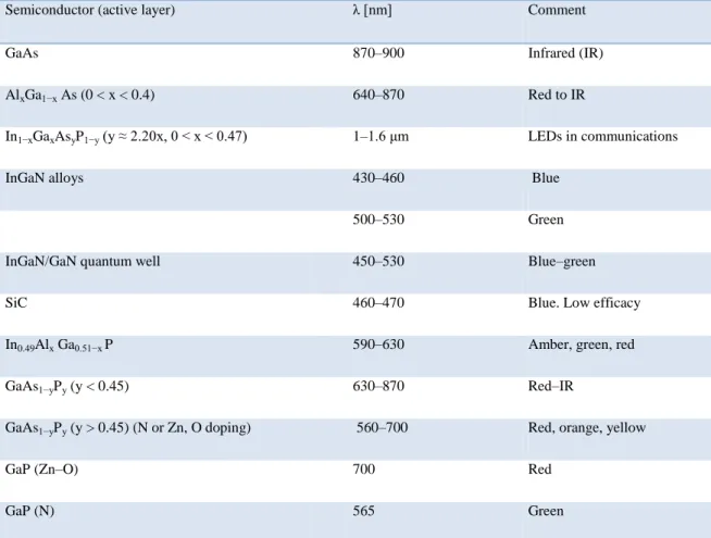
Semiconductor (active layer) λ [nm] Comment GaAs 870–900 Infrared (IR) AlxGa1−x As (0 < x < 0.4) 640–870 Red to IR
In1−xGaxAsyP1−y (y ≈ 2.20x, 0 < x < 0.47) 1–1.6 μm LEDs in communications
InGaN alloys 430–460 Blue 500–530 Green InGaN/GaN quantum well 450–530 Blue–green SiC 460–470 Blue. Low efficacy
In0.49Alx Ga0.51−x P 590–630 Amber, green, red
GaAs1−yPy (y < 0.45) 630–870 Red–IR
GaAs1−yPy (y > 0.45) (N or Zn, O doping) 560–700 Red, orange, yellow
GaP (Zn–O) 700 Red
GaP (N) 565 Green
Table 1.1 Selected LED semiconductor materials, wavelengths of emission in commercial LEDs.
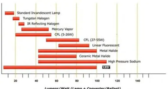
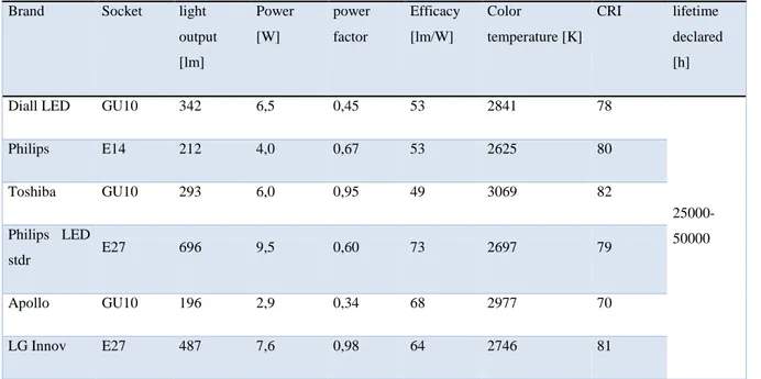
Nowadays LEDs can generate red, yellow, green, blue or white light (semiconductors referring to the colors shown in Table 1.1[23]), have a life up to 50,000 hours, and are widely used in traffic signals and for decorative purposes. White light LEDs are a recent advance and may have a great potential market for some general lighting applications. Their efficacy have already compared with the main commercial lamp products, as shown in Fig. 1.13. Some commercial LED products are shown in Fig. 1.14, which are Diall Spotlight, Philips E14 Spotlight, TOSHIBA Spotlight, Philips Stdr Bulb, Apollo SITA Spotlight, LG Bulb and their main commercial parameters are measured in the lab as shown in Table 1.2. They have become quite good substitute for the incandescent lamp and gas discharge lamp in low power application, such as indoor lighting applications or headlights of vehicles. Although initial costs may seem high to a customer, LED products are actually already a cheaper solution considering their long life and high efficacy. It is clear that LEDs would help to reduce the energy cost for lighting. It is said that 22% of the electricity power in the United States is consumed in lighting and related applications and if the LEDs could substitute for all
21
conventional white light sources in the world, energy consumption could be reduced by around 1,000 TWh per year, as well as reducing greenhouse gas emission by about 200 million tonnes [24].
Fig. 1.13 Efficacy comparison of light sources
22
Brand Socket light output [lm] Power [W] power factor Efficacy [lm/W] Color temperature [K] CRI lifetime declared [h] Diall LED GU10 342 6,5 0,45 53 2841 78
25000-50000 Philips E14 212 4,0 0,67 53 2625 80 Toshiba GU10 293 6,0 0,95 49 3069 82 Philips LED stdr E27 696 9,5 0,60 73 2697 79 Apollo GU10 196 2,9 0,34 68 2977 70 LG Innov E27 487 7,6 0,98 64 2746 81
Table 1.2 The main parameter of the LED samples
As the well known Moore‘s law (which predicts by Moore in 1965 that the performance of microprocessors would double every two years), a similar prediction for LEDs was made by Roland Haitz (2006). It is based on historical data in Fig. 1.15. As currently stated, it predicts that the luminous output of individual LED devices is increasing at a compound rate of 35% per year and that the cost per lumen is decreasing at 20% per year. To the extent that current manufacturers seem to have settled on 3 W as the maximum practical power in a small device, we can read this as also meaning an increase in efficacy of 35% per year. [25]
23
However, there may be two kinds of physical limits for white LED‘s efficacy rise. For the white LED using phosphor, phosphor conversion of white light from LEDs would be limited to about 238 Lm/W (for an acceptable CRI) [25]. Note that since fluorescent tubes are also phosphor-converted, but starting from 235 nm rather than 435 nm, their ultimate efficacy is considerably lower than that of LEDs. Ultimately LEDs will be more efficient than fluorescent lighting. For the white LED combining two or more colors without phosphor, direct emission can be more efficient, because there is no absorption and reemission involved. But since colors other than green are needed to get acceptable CRI, white light cannot be made at higher efficacy than about 350 Lm/W [25]. After the efficacy limit is reached, Haitz‘s law may still apply to the cost per lumen. The figure shows that after 2015 the cost per lumen of LEDs will approach that of 60 W incandescent bulbs.
The total LED efficacy is also described as the external quantum efficiency (EQE), which is defined as below:
EQE=IE*IQE*EE*CE
where IE is the injection efficiency, IQE is the internal quantum efficiency, EE is the extraction efficiency and CE is the conversion efficiency of the phosphor. The IE is the ratio of electrons being injected into the quantum wells to those provided by the power source, the IQE is the ratio of photons generated to the number of electron–hole recombination, and the extraction efficiency is the ratio of photons leaving the LED to those generated. In the case of white-light generation using phosphors, the CE is the ratio of emitted longer-wavelength photons to shorter-wavelength absorbed photons. It could be one for the LED without phosphor. The improvement of EQE is mainly focused on increasing IQE and EE.
The IQE of today‘s best LEDs is at least 75% [26]
and may even be approaching 80%. To make further improvements, firstly nonradiative recombination centres, which help to convert the bang gap energy to heat, need to be eliminated. More importantly, a shift is needed in growing the LEDs, from polar to nonpolar or semipolar crystallographic directions instead, to eliminate strain induced electric polarization fields seen within the quantum wells [27].
When it comes to the extraction efficiency, because of large differences in the refractive indices of air and the semiconductor, such as GaN, a considerable fraction (90–95%) of the generated photons within the LED are trapped by total internal reflection. A popular method is to increase the amount of light hitting the LED–air interface at near-perpendicular values to
24
reduce the occurrence of total internal reflections. For example, as shown in Fig. 1.16 [28], internal reflections can be reduced and hence more light can be collected by shaping the semiconductor into a dome so that the angles of incidence at the semiconductor-air surface are smaller than the critical angle. An economic method of allowing more light to escape from the LED is to encapsulate it in a transparent plastic dome.
Fig. 1.16 (a) normal semiconductor with total internal reflection. (b) domed semiconductor. (c) encapsulation
Generally speaking, increasing the exterior power will give more luminous flux for LEDs except for operating at higher current densities (over 10 Acm–2). When the current through the LED is too high, the EQE would decrease. Although the exact cause has not yet been determined, it is believed that using thicker quantum wells and altering the structure to lessen carrier overflow will reduce this to the point that it will be possible to operate at higher efficacies and currents.
LEDs produce more light per electrical watt than incandescent lamps with the latest devices rivaling fluorescent tubes in energy efficiency. They are solid-state devices, which are much more robust than any glass-envelope lamp and contain no hazardous materials like fluorescent lamps. LEDs also have a much longer lifetime than incandescent, fluorescent, and high-density discharge lamps
Although LEDs possess many advantages over traditional light sources, a total system approach must be considered when designing an LED-based lighting system. LEDs do not radiate heat directly, but do produce heat that must be removed to ensure maximum performance and lifetime. LEDs require a constant-current DC power source rather than a standard AC line voltage. Finally, because LEDs are directional light sources, external optics may be necessary to produce the desired light distribution [29].
25
Nowadays the discharge lamps based on plasma technology are still the take the governing position in the lighting industry. The low luminance efficiency has leaded the incandescent lamp to restrictive governmental legislation [30]. SSLs, in the near future, prove to be a good alternative in some cases, especially as a replacement for incandescent and possibly fluorescent lamps. However, even if LED technology is advancing as rapidly as predicted, electrical discharges will have to supply the major share of light sources for at least another two decades [31], [32], [33]. In any case it is expected that the gas-discharge lamps are mostly qualified for the general illumination of large areas such as sports arenas, buildings and roads.
26
I.3.1 OLED
Fig. 1.17 OLED Early Product
OLED is the acronym of organic light-emitting diode, as shown in Fig. 1.17. It‘s really still an LED in which the emissive electroluminescent layer is a film of organic compound which emits light when the current is passing. This layer of organic semiconductor is located between two electrodes and at least one of these electrodes is transparent so that the light comes out from the active layer. The typical structure of an OLED is shown in Fig. 1.18[34]. A common device structure comprises a glass substrate coated with indium tin oxide (ITO) as transparent anode and a thin, opaque metal film as cathode. Several thin – film layers are deposited on each other and each layer performs a defined function such as generation of specific color or the transportation of electronic charge away from the electrodes towards the organic dopants. The collective aim is to maximize the recombination of electrons and holes and cause organic molecules to emit light. The organic stack including the electrodes is usually thinner than 1 μm. Two classes of organic materials are commonly used for organic light-emitting devices: polymeric substances and so-called ―small molecule materials‖ which do not exhibit any orientating property and therefore form amorphous films.
One interesting aspect of organics-based optoelectronics is the possibility to use simple screen printing or wet deposition techniques for cost-effective fabrication of large-area devices. Nowadays, this applies only to polymeric organics, whereas evaporating techniques still have to be applied for small molecules.
27 Fig. 1.18 The typical structure of an OLED.
When a DC bias is applied to the electrodes, the injected electrons and holes can recombine in the organic layers and emit light of a certain color depending on the properties of the organic material. These materials have conductivity levels ranging from insulators to conductors, and are therefore considered organic semiconductors. Since charge carrier transport in organic semiconductors relies on individual hopping processes between more or less isolated molecules or along polymer chains (Fig.1.19 [34]), the conductivity of organic semiconductors is several orders of magnitude lower than that of their inorganic counterparts. Furthermore, the concept of energetic bands is not applicable to organic electronics. Instead of ―valence band‖ and ―conduction band‖, the relevant terms are ―HOMO level‖ (highest occupied molecular orbital level) and ―LUMO level‖ (lowest unoccupied molecular orbital level). A current of electrons flows through the device from cathode to anode, as electrons are injected into the LUMO of the organic layer at the cathode and withdrawn from the HOMO at the anode. This latter process may also be described as the injection of electron holes into the HOMO. Before actually decaying radiatively, an electron-hole pair will form an exciton in an intermediate step, a bound state of the electron and hole, which will eventually emit light when it decays. This happens closer to the emissive layer, because in organic semiconductors holes are generally more mobile than electrons. The frequency of this radiation depends on the band gap of the material, in this case the difference in energy between the HOMO and LUMO.
28 Fig. 1.19 Diagram of OLED light emission mechanism
As electrons and holes are fermions with half integer spin, an exciton may either be in a singlet state or a triplet state depending on how the spins of the electron and hole have been combined. Statistically three triplet excitons will be formed for each singlet exciton. Decay from triplet states (phosphorescence) is spin forbidden, increasing the timescale of the transition and limiting the internal efficiency of fluorescent devices. Depending on its chemical structure, a dye molecule can be either a fluorescent or a phosphorescent emitter. Only in the latter, all excitons–singlets and triplets are allowed to decay radiatively. Typically, a polymer such as poly (n-vinylcarbazole) is used as a host material to which an organometallic complex is added as a dopant. The heavy metal atom at the centre of these complexes exhibits strong spin-orbit coupling. Phosphorescent organic light-emitting diodes make use of spin–orbit interactions to facilitate intersystem crossing between singlet and triplet states, thus obtaining emission from both singlet and triplet states and improving the internal efficiency. In the former, however, three quarters of all excitons( the triplet excitons) do not emit any light. Fluorescent emitters therefore have a maximum intrinsic efficiency of only 25 % and their application is avoided if possible. However, up to now, the lifetimes of phosphorescent emitters, especially at a short wavelength (blue), are inferior to those of fluorescent ones.
Originally, the most basic polymer OLEDs consisted of a single organic layer (such as polyphenylene vinylene). However multilayer OLEDs can be fabricated with two or more layers in order to improve device efficiency as well as conductive properties. Different
29
materials may be chosen to aid charge injection at electrodes, as shown in Fig.1.20 [35]. The emissive layer (EML) is the source of the light. Other layers that comprise the organic compound are the electron transport layer (ETL), hole transport layer (HTL), and hole injection layer (HIL). Their role is to optimize the flow of the electric current so that the EML's light emission is maximized.
Fig. 1.20 Multilayer OLEDs scheme
Indium tin oxide (ITO) is commonly used as the anode material. It is transparent to visible light and has a high work function which promotes injection of holes into the HOMO level of the organic layer. A typical conductive layer may consist of PEDOT:PSS ( which is a polymer mixture of two ionomers : sodium polystyrene sulfonate carrying negative charges ; poly(3,4-ethylenedioxythiophene) carries positive charges) [36] as the HOMO level of this material generally lies between the work function of ITO and the HOMO of other commonly used polymers, reducing the energy barriers for hole injection. Besides ITO‘s conductivity is lower than the metal‘s, which is about two orders of magnitude lower than that of aluminium. This leads to a significant voltage drop across the transparent electrode and causes variations in the local driving voltage of the active layers depending on the distance to the electrical contacts. Consequently, the emission intensity decreases from the periphery of the device towards its center. In order to lower the lateral voltage drop, thin metal bus lines can be deposited on top of the ITO anode, which increases the mean conductivity of the anode, while shadowing only a minor fraction of the active area and thus yielding a more uniform luminance pattern. Metals such as barium and calcium are often used for the cathode as they have low work
30
functions which are good for injection of electrons into the LUMO of the organic layer [37]. Such metals are reactive, so they require a capping layer of aluminium to avoid degradation. Experimental research has proven that the properties of the anode, specifically the anode/hole transport layer (HTL) interface topography plays a major role in the efficiency, performance, and lifetime of organic light emitting diodes. Imperfections in the surface of the anode decrease anode-organic film interface adhesion, increase electrical resistance, and allow for more frequent formation of non-emissive dark spots in the OLED material adversely affecting lifetime. Mechanisms to decrease anode roughness for ITO/glass substrates include the use of thin films and self-assembled monolayers. Also, alternative substrates and anode materials are being considered to increase OLED performance and lifetime. Possible examples include single crystal sapphire substrates treated with gold (Au) film anodes yielding lower work functions, operating voltages, electrical resistance values, and increasing lifetime of OLEDs
[38]
.
In organic semiconductor technology, electrical doping is used to increase the conductivity of the material and to enhance the carrier injection from the electrodes into the organic materials. This allows for the design of devices with intrinsically undoped active layers embedded in p-type and n-p-type-doped layers, which are therefore referred to as ―PIN diodes‖. In addition to an improved electrical performance, such a design also provides the opportunity to increase the thickness of the device while maintaining the operating voltage almost constant. The overall thickness of the device between the electrodes should amount to some hundred nanometers to provide sufficient protection against electrical short-circuits. These are often caused by the presence of particles on the substrate during evaporation of the organic layers or by the roughness of the substrate.
Doping also enables a series connection of several active layers in a higher-stacked structure (Fig.1.21[34]). An intermediate PN junction operated in reverse direction behaves like a tunnel contact: the carriers can directly pass from the HOMO level of one layer to the LUMO level of the adjacent layer. In the OLED community, these junctions are often called ―charge generation layers (CGLs)‖ because electron-hole pairs are created at the interface and separated by the field. The equivalent circuit of a large-area device is a series connection of three resistors, representing the anode, the organic layers and the cathode. The higher the differential resistivity of the organic layers at the operating point, the lower is the voltage drop across the electrodes which results in an enhanced uniformity. As stacked device architectures
31
have a much higher differential resistivity, stacking is a way to increase the uniformity and output of large-area devices without having to apply bus lines.
Fig. 1.21 Stacked device architecture
A device structure with immanent series connection is referred to as ―stacking‖. A twofold white stacked device, for example, can basically achieve the same luminance levels as a simple device – at half the current, since there are two emitting units, but at twice the voltage. Compared with simple PIN devices, stacked device architectures offer several advantages in terms of lifetime, optical performance etc.
The organic layers have to be protected against air as they are sensitive to moisture and oxygen and decompose when exposed. A possible encapsulation technique is shown in Fig. 1.22[34]. A thin but dense amorphous oxide layer is deposited onto the cathode, which provides a sufficient permeation barrier. Due to its thinness, this thin-film encapsulation (TFE) has to be protected from mechanical damage, for example by laminating an additional glass layer onto it, by applying a lacquer coating etc.
32
\ Fig. 1.22 Thin film encapsulation
Typical emission spectra of organic molecules are broad (as shown in Fig.1.23 [34]). As stated before, the emission color is a material property. Thus, the total emission can be tuned to virtually any color, including white at any color temperature, by stacking several different emitting layers in a single device. This is possible since the organic layers are almost transparent in the visible spectral range. Most white OLEDs contain a red, a green and a blue emission layer to create high-quality white light.
Fig.1.23: Typical emission spectra of organic materials. The diagram shows spectra of red, green and blue emitters and their superposition which yields white emission at a high color rendering index.
During the lifetime of an OLED, the luminance will decrease monotonically at constant current. The resistivity and thus the operating voltage will increase accordingly. The lifetime scales super-linearly with both the emitted radiation intensity (or current density) and the
33
temperature. The temperature, in particular, has to be considered when designing OLED based luminaires. At high luminance levels, large-area devices may have considerably elevated temperatures during operation and the possibility of heat exchange with the surroundings should be provided in order to ensure a long lifetime of the device. In this case, stacked device architectures once again offer the possibility to lower the individual emission of each unit, thus slowing down their aging mechanisms, while keeping the overall emission constant.
OLEDs are very good flexible glare-free area light sources with high color quality. When turned off, they can be transparent or have either a mirror-like or milky appearance. They can be very thin and lightweight, and turned on instantly. OLEDs have the potential to be equally or more efficient and long-living than fluorescent lamps, while being 100 % mercury-free and no UV and IR radiation. As a kind organic material it is easy to realize the low cost production as the other plastic film. However, on the other hand, organic materials are not as robust as the inorganic material and degrade by the water and the oxygen, which always limits the performance and the lifetime of OLEDs. Besides faster degradation is occurring in the blue OLEDs that are required to be used in company with the red and green OLED in order to produce white light.
In the near future, OLEDs could be wild used displays devices, such as television screens, computer monitors, and portable systems. An OLED display works without a backlight; thus, it can display deep black levels and can be thinner and lighter than a liquid crystal display (LCD) [39].
I.4 The Work of This Thesis
The subject of our work is a mercury free gas discharge lamp, the flat dark discharge lamp (FDDL). It is filled with lower pressure gases (below 1 Torr), and operated with voltages in the range of 1.7 - 4 kV DC and currents of 0.5 - 1 mA. When it works normally no obvious visible light comes from the discharge chamber and only the luminance of cathodoluminescent (CL) phosphor could be observed (so called dark discharge lamp). It would be convenient to work as the backlight for the LCD owing to its shape. Fewer gas atoms or molecules cannot support a saturate propagation of electron and ion production, which limit the capability of charge transportation and keep the voltage higher and current lower than the normal fluorescent lamp. But with high lamp voltage and few collisions
34
electrons could be accelerated to high velocity and make phosphor bright. After breakdown progress the population of electrons rises exponentially, and the FDDL turns on.
Further introduction of our lamp and some basic numerical calculation are introduced in Chapter II, in which the excitation and ionization mean free paths are used to analyze the physics behind the threshold pressure for the FDDL. Traditional discharge lamps work under glow or arc discharge regimes, while the lamp we studied functions in the regime between Townsend discharge regimes and glow discharge region. Further introduction to the special characteristics of FDDL are present in chapter II.2.
In such a narrow gap and low pressure, there may be no adequate collisions happening before charged particles reach electrodes. The mean free path, diffusion model and Townsend discharge theory are introduced in chapter II.3. Fluid equations and Townsend discharge theory could help to understand physics insides and give the possible space charge distribution. Mean free path presents the collision possibility, which helps to explain the special working condition for this application in chapter II.4. As the cross sections distribution of excitation and ionization are different, when the discharge gap is limited, there would be some condition which is good for ionization and bad for excitation.
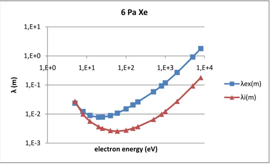
Some feathers of the sample lamps are explored in chapter III. And the experiment result of FDDL at different pressure filled with Neon and Xenon are also present and discussed in that chapter. Experiments are operated on the sample and empty FDDLs. From the sample tests, some characteristics of the FDDL have been revealed in chapter III.2 including the phosphor performance (the response of the phosphor to different wave length incident photons) and the uniformity of the lamp. It will help to fully understand the characteristics of this type of brand new light sources. In chapter III.3, the empty lamps are filled with different pressure neon to present the lamp behavior with different pressures and input powers. Low pressure and high input power would help to improve the lamp application. Xenon is also filled as buffer gas to compare the turn on voltage with that of Neon. The V-I plot could help to prove its difference from the field emission. In the commentary chapter, some failures and problems are revealed and possible reasons are discussed.
I.5 Summary
Electrical light sources have been developed for about 200 years. There are three generation light source: incandescent lamp, discharge lamp and solid state lamp. The incandescent lamp