HAL Id: hal-01207499
https://hal.archives-ouvertes.fr/hal-01207499
Submitted on 1 Oct 2015
HAL is a multi-disciplinary open access
archive for the deposit and dissemination of
sci-entific research documents, whether they are
pub-lished or not. The documents may come from
teaching and research institutions in France or
abroad, or from public or private research centers.
L’archive ouverte pluridisciplinaire HAL, est
destinée au dépôt et à la diffusion de documents
scientifiques de niveau recherche, publiés ou non,
émanant des établissements d’enseignement et de
recherche français ou étrangers, des laboratoires
publics ou privés.
Reliability of Sigma-Delta modulator
Hao Cai
To cite this version:
Hao Cai. Reliability of Sigma-Delta modulator: Reliability. [Research Report] Telecom Paristech.
2012. �hal-01207499�
Rapport d’Evaluation `a Mi-parcours
Hao Cai
Th`ese: Fiabilisation de convertisseurs analogique-num´erique versatiles `a modulation
Σ∆
Directeurs de Th`ese: Jean-Franc¸ois Naviner, Herv´e Petit
T´el´ecom Paristech
October 2, 2015
Abstract
With the continuous scaling down of CMOS technology, reliability problems such as ageing effect induced parameter degradations and process variation become critical aspects and major bottleneck in integrated circuits (ICs) design. Their joint effects impact the ICs performance and service lifetime. Traditionally, according to specifications, ICs are often designed conservatively to ensure fabricated systems can meet reliability goals, which leads to a reduced performance. New design-for-reliability (DFR) loop and variability-aware methodolo-gies need to be developed for sub-micron technology. Analog-to-digital sigma-delta modulators (Σ∆Ms) is the object of study in this thesis. Physical mechanisms of time dependent ageing degradation (NBTI, HCI, TDDB) and process variation are investigated. Reliability analysis onΣ∆Ms is performed with 65 nanometer CMOS technology. Information such as system lifetime, sensitive blocks and weak spots must be evaluated. Statistical analysis for process variations is implemented by using DoE-RSM method. Design methodologies using behav-ioral modeling, nominal simulation, hierarchy circuit design and quadratic response surface modeling applied to analog/mixed integrated circuit is proposed and validated.
Index Terms: Ageing degradation, Design-for-reliability, Process variations, CMOS 65 nanometer technology, Sigma-delta modulator, Behavioral modeling, Quadratic response surface modeling, Hierarchy circuits design.
1
Reliability issues
In semiconductor industry, as CMOS technology continuously scaling down, the increasingly minute IC system have achieved high integration and low power. However, problems such as leakage current, noise and drain induction barrier lower (DIBL) came on the heels. One of the major issues is IC reliability. Process induced variations and time-dependent degradations of transistors significantly impact circuit performance. According to the ITRS Roadmap [1], small devices combined with new materials will deeply affect the design of next generation of integrated circuits.
Generally, reliability is defined as the ability of a certain circuit to conserve a given functionality during specified time duration under certain environments. The capability of circuit or system reliability becomes an essential performance of circuits and plays a role as a new element in the design tradeoff between power, di-mension, specification, etc. Nowadays, both reliability-aware and variability-aware circuit design are hot topics. For reliability, we need to design ICs with tolerance to ageing degradations; for product yield, the proportion of fabricated circuits which can meet the design specifications is also an important indicator. In conventional IC manufacturing process, in order to achieve high yield and reliability, the redundancy design is a extensively accepted methodology. Even if ICs are suffering from yield and reliability degradation, the circuit performance still can satisfy the design requirement. In other words, the performance of designed circuits (larger chip area and high-power) are exceed the design target [2].
Despite of the complexity of new integration schemes, recent published papers did not emphasized a signifi-cance on transistor ageing degradation, process variations (neither local nor global) and circuits reliability. This thesis focuses on reliability and variability modeling, design methodology, circuit analysis and yield estimation of versatile sigma-delta analog-to-digital converters (Σ∆-ADC) with CMOS technology. Section 2 and 3 illus-trate methodologies and make analysis of temporal and spatial reliability problems separately, emphasis is laid on time-dependent ageing degradations and circuit statistical design for yield. Relevant work on sigma-delta modulator is also demonstrated in these two sections. Section 4 makes some intermediate conclusion on vari-ability and relivari-ability aware design and methodologies. Finally, perspective and future work are given in section 5.
Figure 1: General electric fields in MOS transistor
2
Temporal reliability issues
2.1
Ageing effect mechanisms
Due to aging phenomena, transistor devices can be affected by temporal reliability problems. They are typ-ically Negative Bias Temperature Instability (NBTI), Hot Carrier Injection (HCI), Time Dependent Dielectric Breakdown (TDDB) and Electromigration (EM). The time-dependent degradation effects, include NBTI, HCI and TDDB, they will cause a change of transistor parameters (e.g., VT,β, ro) as a function of time and therefore
might turn an initially fully functional circuit into a less or even non-functional circuit over time [3].
2.1.1 Negative bias temperature instability
NBTI refers to the generation of positive oxide charge and interface traps at the Si-SiO2interface under
nega-tive gate bias, in particular at elevated temperature. When neganega-tive gate bias is applied to PMOS, the transverse electric field (ET) is generated (see Figure 1). NBTI manifests itself as a shift of threshold voltage in PMOS
tran-sistors, especially in high temperature. Depending on the bias condition, two phases are defined: stress phase (or static NBTI) and recovery phase. Dynamic NBTI corresponds to the case where the PMOS transistor undergoes alternate stress (e.g., Vgs= - Vdd) and recovery (Vgs= Vdd) periods. At system level, the effective techniques to
mitigate the NBTI degradation are supply voltage tuning, PMOS sizing and duty cycle reducing [4] [5]. Besides NBTI, positive bias temperature instability (PBTI) also affects CMOS transistors especially in sub-32 nanometer CMOS. For evaluating the degradations, the reaction-diffusion (R-D) model is widely used [4], which can inter-pret the power-law dependence of interface trap generation at the Si-SiO2interface. Some limitations exist in
R-D model, like frequency-dependency of NBTI. Recent published work [6] shows a contradictory observations that BTI is not frequency-dependent (at least for measurements up to 3 GHz).
2.1.2 Hot carrier injection
HCI emerges from the shrinking of transistor dimension and the electric field increasing in the channel. When HCI happens, hot electrons overcome the potential barrier and inject into gate oxide due to high lateral electric field (EL) near the drain (see Figure 1). HCI causes the generation of the interface traps at the Si-SiO2interface
near the drain when the transistor switch on, the Vgd is greater than or equal to zero and the Vgsis high enough.
It results in threshold voltage and electron mobility degradation which can not be recovered [4] [7]. Reliability effects result in poor drive current, low noise margin, which can shorter device and circuit lifetime [8] [9]. The scaling down of CMOS technology brings in supply voltage reduction, the relative lower drain current will reduce HCI effects [10]. However, this is not always feasible, since when gate lengths less than 50nm, no significant reduction in gate voltage is planned for additional scaling. On the other hand, noise and output charge represent a more important constraint in most design cases [11].
2.1.3 Time dependent dielectric breakdown
The breakdown is caused by defects generated in gate dielectric that subsequently form a percolating path through the oxide and electrically short the gate to the substrate [12]. The mechanism that causes time dependent di-electric breakdown begins with an electron tunneling through the oxide. Different breakdown modes, such as Hard-BD (HBD), Soft-BD (SBD), Progressive-BD (PBD) were distinguished according to the thickness of the gate oxide [3]. The most harmful mode is HBD, which can cause a catastrophic failure of the device and conse-quently, of the entire circuit. SBD can evolved to HBD which has smaller effect on circuit operation. Compared to the resistor-like HBD, the conductance of SBD is limited and strongly non-linear. With a reduction in power supply voltage, the formation of the first percolating path no longer leads to transistor failure; indeed, the devices
Figure 2: The design for reliability (DFR) flow
are now capable of sustaining multiple SBD paths, before undergoing an irreversible HBD.
2.1.4 Electromigration
Apart from the time-dependent degradation effects, electromigration caused by excessive current density stress in the interconnect must be considered in both design and layout step. A EM aware physical design flow [13] has been implemented. Three modules (current-driven routing, current-density verification and current-driven layout decompaction) have been developed to address EM relevant physical design constraints.
Since each ageing phenomenon is caused by its relevant physical mechanism, it is necessary to analyze com-bined effect of different ageing phenomena. It is also essential to develop effective reliability-aware simulation methodologies which can deal with different mechanisms.
2.2
Reliability-aware simulation methodologies
Traditionally, reliability analysis is performed on fabricated ICs after taping out. If reliability problems were occur, circuit redesign is needed. Considering IC’s time-to-market, a design for reliability (DFR) flow (see Figure 2)is introduced in the circuit design phase, prior to layout. Reliability-aware simulation is used to predict the ageing effects of degradation mechanisms on electronic systems [14], .
The earliest reliability simulation method is DC modeling reliability simulation by SPICE-like simulators, which have been developed at the beginning of 1990 [15], [16]. The disadvantage of DC modeling is its low accuracy and inefficiency for complex circuits [17]. Bestory et al [17] proposed a reliability simulation method-ology by circuits behavioral aging modeling. Behavioral modeling is a possible solution to achieve simulation computational efficiency especially in complex systems. Figure 3 shows the ageing effect modeling at device level. Circuit behavioral modeling is the possibility to build a behavioral electrical model of a circuit or system to speed up the simulation.
Nominal ageing simulation is a popular used method because of its high accuracy and accessibility. In Figure 4, a transient simulation is performed on the input netlist. The stress on every transistor node is calculated and passed to a degradation model. The degradation is extrapolated at a certain circuit operation time. Finally, a degraded circuit netlist is created as an output. Ageing degradation of circuit performance can be evaluated. Typically, some commercial reliability simulators such as RelXpert, Virtuoso UltraSim and Eldo which can generate aged netlists from their ageing models are used for nominal simulation.
Table 1 lists the comparison between methodologies mentioned above. Besides the simulation accuracy and speed, compatibility and accessibility are taken into consideration. A methodology is said to be compatible if it can be applied on one of the systems can also be run on other systems. Accessibility describes the degree of a methodology that whether it is available to as many designers as possible or not. We find that nominal simulation methodology is with high accuracy and compatibility and can be easy to access by designers. The behavioral modeling is suitable for complex system ageing simulation because of its fast speed. Last but not least, the
Figure 4: The nominal ageing simulation flow
DC only analysis Behavioral model Nominal simulation
Accuracy low reasonable high
Speed fast fastest reasonable
Compatibility reasonable low high
Accessibility low low high
Table 1: Comparison between reliability methodologies
DC only reliability method is suitable for modeling some ageing effects (TDDB and EM) which have not been modeled in commercial tools.
Considering the advantages of nominal ageing simulation method and ageing behavioral modeling, we de-signed a reliability-aware simulation methodology and study it in analog-to-digital sigma-delta modulator.
2.3
Reliability-design of
Σ∆ modulators
TheΣ∆ modulator (see Figure 5) is a key component in many mixed-signal integrated circuits. Normally, the robustΣ∆Ms are benefit from the negative feedback path. When the gain a of analog loop filter has a variation δa, the fluctuation of transfer function A in the close loop is:
δA= δa (1 + a f )2 (1) δA A = δa/a (1 + a f ) (2)
Where f is feedback coefficient of D/A, δAA is the sensitivity of transfer function A to variations. The negative feedback can weaken the impact of such fluctuation to a certain degree and increase the system reliability.
However, in some critical applications such as medical science and space technology, the performance of Σ∆Ms is susceptible to ageing effects, process and environment variation. Since it is not efficient to perform reliability analysis on a flat transistor level, designers must recur to some methodologies to solve reliability prob-lems and improve the system. For aΣ∆ modulator or Σ∆ ADC, no matter what kind of circuit reconfiguration, it is remarkable that analog loop filter (integrators), quantizer (comparator) and DAC (digital-to-analog converter) are component units. Here, a methodology based on hierarchical behavioral modeling ofΣ∆Ms with nominal reliability simulation flow will be introduced.
2.3.1 The hierarchy-behavioral modeling methodology
[14] proposed a hierarchy-behavioral modeling methodology (see Figure 6) to study the ageing degradation by nominal ageing simulation with hierarchical behavioral modeling. The nominal ageing simulation is performed
Figure 6: Hierarchy method used inΣ∆Ms[2]
Figure 7: Modeling non-idealities in 2ndorder CT-Σ∆Ms
between transistor and circuit level. Designers can use the output degraded netlist to study the impact of degra-dation on the circuit parameters. At system level, the system performance is evaluated by circuit behavioral modeling.
With NBTI and HCI degradation model, time-dependent degradation is evaluated by nominal transient sim-ulation. The degradation information is transmitted to circuit level as the non-idealities parameters. Finally, both t0(fresh) and aged system performance can be simulated with behavioral modeling. This method integrates
be-havioral ageing modeling and nominal simulation, avoids the disadvantage when using one of the methods above exclusively. It guarantees the speed of ageing analysis by behavioral simulation and enhances ageing simulation accuracy which benefits from nominal transient simulation.
2.3.2 Circuits behavioral modeling
A hierarchical behavioral model of a continuous time (CT) low orderΣ∆M was developed with MATLAB and Cadence tools. In [18], a low power CT-Σ∆M was implemented with 65 nanometer CMOS technology which can be applied for cardiac pacemaker. The second-order modulator follows the CIFB (cascaded of integrators with distributed feedback) architecture, comprises a second-order resistor-capacitor (RC) operation amplifier (op-amps) based loop filter and 1-bit internal quantizer operating at 32 KHz. Return-to-zero (RZ) DAC in feedback path and clock phase generator are integrated. The CT-Σ∆M achieves 45.3 dB SNR, 7 ENOB and 47.3 IM3 with an OSR of 32.
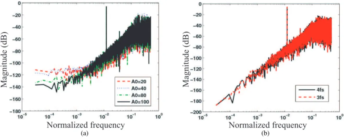
The proposed 2nd-order LP CT-Σ∆M is in cascade of integrator with distributed feedback and input coupling (CIFB) structure (see Figure 7). The non-idealities parameters, such as DC gain (Adc), gain bandwidth (GBW )
and loop delay are modeled with Verilog-AMS at circuit level. Figure 8(a) 8(b) demonstrates that when nonideal Adcand GBW happen in op-amps, the output spectrum will be worse. SQNR is 55.0 dB, 55.0 dB, 54.5 dB, 51.3
dB when Adcis 100, 80, 40 and 20; SQNR is 54.9 dB, 54.8 dB when GBW is 128 kHz and 96 kHz.
With infinite GBW , the SQNR is almost the same when DC gain is larger than 40 (linear) (see Figure 9). Meanwhile, with infinite DC gain, the SQNR will become worse if GBW is lower than 3* fs. In order to satisfy
design requirement, we choose Adc= 40 (linear) and GBW = 96 kHz(3* fs) as the parameter of op-amps in the
loop filter.
The excess loop delayαTclkis set in order to guarantee a decision time to quantizer, whereα = 0.25. Excess
loop delay arises because of nonzero transistor switching time, which makes the edge of the DAC pulse start after the sampling clock edge. The CT-Σ∆M is very sensitive to feedback waveform generated from the DAC. The excess loop delay in feedback loop can affect the noise transfer function (NTF) and then influence the modulator performance.
The SQNR, signal-to-noise and distortion ratio (SNDR) and spurious free dynamic range (SFDR) are con-sidered. According to the simulation result, there is no degradation if the delay happens in quantizer (see Fig-ure 10(b)). If the delay occurs in the feedback loop (see FigFig-ure 10(a)), when delay time is below 20% of Tclk,
the SQNR is roughly a constant. However, the performance degrades as delay increases. In DAC, there will be serious degradation when the excess loop delay exceeds 0.3Tclk.
Normalized frequency
Magnitude (dB
)
(a)Normalized frequency
Magnitude (dB
)
(b)Figure 8: Output spectrum with DC gain and gain bandwidth variance.
0 50 100 150 200 250 0 10 20 30 40 50 60 70 80 90 100 OSR SNR(dB)
2nd−order SDM with fs=2MHz; Fin=31*fs/N; Amp=−10dB
A0 = 10 A0 = 50 A0 = 100 A0 = 1000 A0 = 100K
Figure 9: SNR with different OSR and op-amp DC gain
0 0.1 0.2 0.3 0.4 0.5 0.6 0.7 0.8 0.9 1 0 10 20 30 40 50 60 70
Excess loop delay (normalized to Ts)
Magn
itude (dB)
2nd−order CT−SDM with fs=32KHz;Fin=400Hz, ain=400mV SNR SNDR SFDR (a) Quantizer 0 0.05 0.1 0.15 0.2 0.25 45 50 55 60 65 70 75 80
2nd−order CT−SDM with fs=32KHz;Fin=400Hz, ain=400mV
Quantizer delay time (normalized to Ts)
Magn itude (dB) SNR SNDR SFDR (b) Feedback loop
Figure 10:Σ∆M performance versus excess loop delay
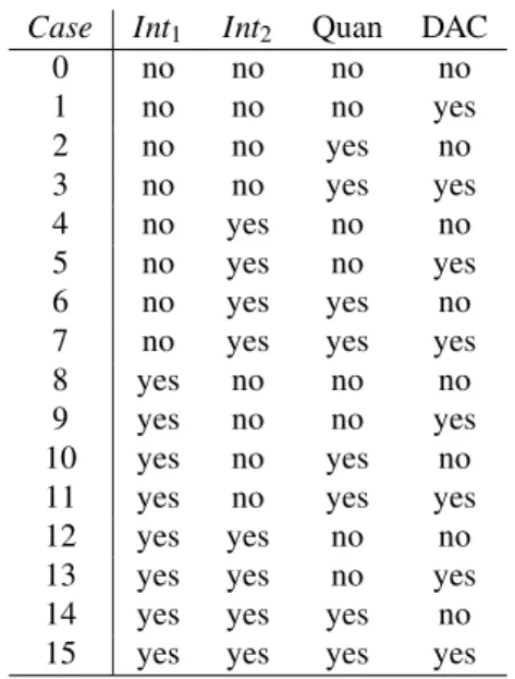
2.3.3 Weak spot detection
Evaluating weak spots in a circuit or system is an important step in reliability simulation. Designers can improve reliability and decrease overdesign. Behavioral model of blocks inΣ∆ converter will be built by Verilog-AMS language. We divide the modulator into the first integrator (Int1), the second integrator (Int2), quantizer (Quan) and DAC. There are 16 test cases of failure estimation (see Table 2). The failure condition of integrators (op-amps) is set as a 3 dB loss of DC gain and 32 KHz degradation of GBW. For the latched comparator and return-to-zero (RZ) DAC feedback circuit, we consider the excess loop delay as non-ideal parameter. 0.25 Tclk
Case Int1 Int2 Quan DAC 0 no no no no 1 no no no yes 2 no no yes no 3 no no yes yes 4 no yes no no 5 no yes no yes 6 no yes yes no
7 no yes yes yes
8 yes no no no
9 yes no no yes
10 yes no yes no
11 yes no yes yes
12 yes yes no no
13 yes yes no yes
14 yes yes yes no
15 yes yes yes yes
Table 2: Failure test cases ofΣ∆ converter
Figure 11: PW and PP error induced by ageing effects
circuit. This methodology has been applied in [14], [18]. The result shows that feedback loop is the weak spot in the second order CT-Σ∆M.
2.3.4 Reliability analysis on clock unit in CT-Σ∆M
CTΣ∆Ms are benefit from anti-aliasing filter and speed/power advantages over their discrete-time (DT) coun-terparts. However, CT Σ∆Ms are suffered problems induced by clock uncertainties. In CMOS 65 nanometer technology, it has been verified that ageing effects induced degradation can influence the clock phase gener-ator in CTΣ∆Ms. Figure 11 shows the ageing degradation induced error in the clock unit of CT-Σ∆M with return-to-zero (RZ) feedback . This error is due to variations of feedback pulse width (PW) and pulse position (PP).
Since degradation of quantizer can be shaped by NTF, ageing induced PP and PW error is dominant in feedback loop. The area of feedback pulse is directly linked to average feedback current (IFSI) ofΣ∆Ms. Where
FSI is defined as the maximum average feedback current of the Σ∆M. Correspondingly, FSI in voltage can be defined to be equal to Vre f. With a 1.2V supply, we may take VFSI = Vre f = 0.6 Vpk.di f f. The modulator
performance will be affected by relevant Vre f as:
SQNR≈1.76 + 20Log(Vin Vre f
) + 6.02n + 10Log(2L + 1) − 9.9L + (6L + 3)ln2(OSR) − 20Log(π) (3)
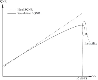
The equation shows the SQNR of Σ∆M is determined by the modulator order L, the number of bits of the quantizer n, the oversampling ratio OSR, the input amplitude Vin and reference voltage Vre f. As shown in
SQNR Vin Instability Ideal SQNR Simulation SQNR -6 dBFS
Figure 12: System performance versus Vin
Parameter 2
Parameter 1 IC Performance
Performance Boundary
Figure 13: IC performance influenced by process variations
Figure 12, the variation of Vre f has an impact of modulator stability. For small input, the SQNR is lower than
predicted (dashed line). PW and PP error can cause Vre f degradation. Reducing Vre f has a risk to bring the
modulator system into instability region.
From behavioral simulation, it was found that a 1.5% PW error can cause 1 dB SQNR loss in the modulator mentioned above. It has been simulated that HCI influences the rising and falling edge randomly. As distinct from HCI, NBTI mechanism can narrow the width of feedback pulse as a PW error, which can decrease the Vre f and impact the SQNR. However, the reliability simulation on transistor level shows that with 1.8V supply
voltage, 150◦C, the NBTI degradation caused PW error is only 0.25 %. The circuit is in a reliable margin.
Last but not least, simulation concerned on NBTI effect of clock unit shows the degradation of circuit has non-frequency-dependent characteristic.
3
Spatial reliability issues
The spatial reliability problems include process variation (global variations and local variation) and random variations (such as oxide thickness variation, line edge roughness, random dopant fluctuation). In this section, we focus on process variation caused IC yield problems.
3.1
Process variations
Integrated circuits are influenced by process variation during manufacturing. As shown in Figure 13, the variation of process parameters can cause fluctuation of ICs performance. The dashed area gives the accepted performance boundary where we calculate the yield information. Although lots of advanced fabrication techniques have been used in modern IC manufacturing process, inherent systematic or random process variations are still existing during each fabrication step. Due to technology continuous scaling down, the impact represents a trend of accelerated increasing.
There are two principal sources of variability: environmental variations, which depend on the operating con-dition such as supply voltage and temperature variation; physical parametric process variation, which including statistical manufacturing tolerances (inter-die variations) and mismatches (intra-die variations). Inter-die
varia-Parameter 2
Parameter 1 3σ design
overdesign due to corner-based design
Figure 14: Corner-based and statistical design against process variability
tions (also refer to global variation) exist in lot-to-lot, wafer-to-wafer and die-to-die. Inter-die variations affect all transistors of a given circuit simultaneously and equally in a same way, result IC performance discrepancy of different chips in identical products. Intra-die variations (also refer to local process variation) are deviations occurring with a die. It represents as local mismatch variations. Apart from process variation, factors such as fluctuation of supply voltage and temperature can also impact ICs performance.
3.2
Statistical design: the state of art
Generally, three yield-aware design methodologies exist, Monte-Carlo (MC) simulation, worst case corner design and statistical design. Their tradeoff are simulation accuracy and efficiency.
MC method is used widely to predicts the parameter fluctuation with a probability distribution. MC-based techniques are inherently accurate as they do not involve any approximation. In practice, MC simulation performs at a low level, demands excessive amounts of computer time, especially when combined with computationally intensive reliability. In traditional MC sampling, a large number of simulation iterations is required to achieve a reasonably precise estimation of the yield. Advanced sampling techniques such as, the stratified sampling, Latin Hypercube Sampling (LHS) and Quasi Monte-Carlo (QMC) are proposed in some digital circuit [19], [20], which can achieve a faster convergence rate in MC-based timing analysis. Beside these MC-based method, some non-MC based variability analysis methods which based on analyzing the linear sensitivity of performance metrics with respects to mismatch parameters and calculating the total metric variance as the sum of the square of each linear component is proposed. In [21], a non-Monte-Carlo mismatch analysis method based on pseudo-noise modeling and PNOISE analysis is published. Device mismatch is modeled as low-frequency pseudo-noise and the variation in performance is derived from the PNOISE simulation results.
The most pragmatic solution to evaluate the circuit performance is corner based design [22], which has been used in design for yield (DFY) for decades. The worst case corner models are generated by offsetting the selected parameters by a fixed number of the performance standard deviations. The designer need to specify the worst-case corners of relevant circuits. For example, the saturation currents and threshold voltages of transistor (maximum or minimum) are used to define worst case corner models: FF, FS (fast NMOS and slow PMOS), SF, SS and TT. FF model stands for fast NMOS and fast PMOS, which can achieve low Vth, tox,∆W and high
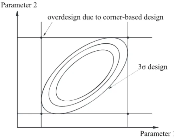
∆L. SS model can determine the transistor performance in opposite directions. Obviously, the worst case corners analysis has limitation in over-estimation or under-estimation of process variations. Hence, the current trend is to move towards true statistical yield optimization, where the statistical distribution of the parameter variations is considered. The difference between corner-based and statistical design against process variability [22] is shown in Figure 14.
Statistical design is needed due to the process parameters variations in the manufacturing and circuit/device performance varying. Designers are interested in finding a exact (or well approximated) statistical distribution of the performance in order to get the information of yield. Unfortunately, direct measurement of process variations at the circuit level is nearly impossible. Therefore, some methodologies measure variations by relating the total contributions of the underlying process variations to a measurable circuit metric. Many approaches for calculat-ing current variations begin with I − V measurements. The model used for these analysis range in complexity from BSIM to the basic square-law model. Pelgrom et al. [23] described current variations as a function of vari-ations in the process parameters VTandβ. Static timing analysis (STA) is a high efficient method to characterize
the timing performance [24] of digital circuits. The NBTI aware STA framework established in [4] can make statistical prediction of digital circuit aging under process variations. Recently, hierarchical statistical analysis has been used to solve the inefficiency of MC simulation. Hierarchical method of statistical analysis based on Lookup Table (LUT) or response surface modeling (RSM) forΣ∆ ADC are proposed in [25] [26], which can
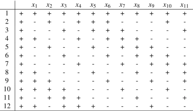
x1 x2 x3 x4 x5 x6 x7 x8 x9 x10 x11 1 + + + + + + + + + + + + 2 + - + - + + + - - - + -3 + - - + - + + + - - - + 4 + + - - + - + + + - - -5 + - + - - + - + + + - -6 + - - + - - + - + + + -7 + - - - + - - + - + + + 8 + + - - - + - - + - + + 9 + + + - - - + - - + - + 10 + + + + - - - + - - + -11 + - + + + - - - + - - + 12 + + - + + + - - - + -
-Table 3: Plackett Burman design: 11 two-level factors for 12 runs.
achieve a good tradeoff between computational efficiency and accuracy in complex circuit performance metric.
3.3
Hierarchical Statistical design
Statistical design is used to identify the most sensitive process parameters along with experimental verification with fewer data points and less simulation time. Here, we introduce hierarchical modeling to circuit statistical design:
[p1, p2, · · · , pn] = F [b1, b2, · · · , bm] (4)
where B= [b1, b2, · · · , bm] is the set of parameter at low level (e.g., physical level), P = [p1, p2, · · · , pn] is the set
of performance at high level (e.g., system level). The link between P and B is defined as F .
3.3.1 Screening and regression analysis
The Plackett-Burman designs are a kind of fractional factorial designs, which have the following orthogonal property [27]: for any given two columns in the experiment design matrix, there are N/4 plus signs and N/4 minus signs in the first column corresponding to N/2 plus signs in the second column. Similarly, for N/2 minus signs in the second column, there will be N/4 plus and N/4 minus signs in the first column. Provided that all the interaction effects are negligible, designs with this property allow unbiased estimation of all main effects of N-1 variables with smallest possible variance. The goal of PB design methodology is to find experimental designs for investigating the dependence of some measured quantity on a number of independent factors. As shown in Table 3, hadamard matrix is used for generating orthogonal 12 times 12 matrix for 11 parameters whose elements are all either plus signs or minus signs (Plus signs (+) represent factors with maximum values; minus signs (-) for minimum values). In this case, only 12 runs are needed with Plackett-Burman designs. A full factorial design would require 211= 128 runs.
In statistics, linear regression is an approach to model the relationship between groups of variables. Sup-pose there exists a relationship between a dependent variable P and a set of m independent variables B, P= f (b1, b2, b3, · · · , bm), where some factors in ˜b have little effect on P. Based on the statistical significance in
a regression, stepwise regression is a method to build multiple linear regression models between P and ˜b which can make hypothesis testing for this model and every independent variable. The steps in the regression add the most significant factor or remove the least significant one until the regression reaches a local minimum of root mean square error (RMSE).
The method begins with an initial model and then compares the explanatory power of incrementally larger and smaller models. At each step, the p value of an F-statistic is computed to test models with and without a potential term. If a term is not currently in the model, the null hypothesis is that the term would have a zero coefficient if added to the model. If there is sufficient evidence to reject the null hypothesis, the term is added to the model. Conversely, if a term is currently in the model, the null hypothesis is that the term has a zero coefficient. If there is insufficient evidence to reject the null hypothesis, the term is removed from the model. Finally, the most optimum regression equation can be built with most significant factors [28]. The p-value, partial F-values and R2value can be used to set a certain threshold to test the hypothesis of regression model.
3.3.2 Design of experiment and response surface modeling
Design of experiment (DoE) is used to estimate the causal impact of the input factors on the output parameters. In process variation analysis, it is used to build the mathematics model between process parameters and system
performance. Comparing with MC method, with DoE fewer data points are needed by choosing proper DoE categories, but the analysis accuracy is still guaranteed. Designers need to choose right DoEs depending on the application data. Commonly used DoE are full factorial designs, fractional factorial designs and optimal designs. The Central Composite design (CCD) and the Box-Behnken design are the most popular types. Box-Behnken design is approximately orthogonal which can achieve high efficiency when there is limited number of factors. When the number of factors is more than 4, the CCD is preferred. CCD such as classical (CCC), inscribed (CCI) and face centered(CCF) are different in range and rotation of factors. The CCD is an experimental design used in response surface methodology (RSM), for building a second order (quadratic) model for the response variable without needing to use a complete full factorial experiment. Since using linear model between process parameter and system performance is not enough accurate, quadratic model (5) or even cubic model (6) is required:
ˆ
y= a0+ a1x1+ a2x2+ a3x3+ a12x1x2+ a13x1x3+ a23x2x3+ a11x12+ a22x22+ a33x23 (5)
ˆ
y′= ˆy+a123x1x2x3+a112x21x2+a113x21x3+a122x1x22+a133x1x23+a223x22x3+a233x2x23+a111x31+a222x32+a333x33
(6)
3.4
Design for yield with BSIM4 process variation
Statistical parameters (eg, in BSIM4 model), have variations that are usually modeled by Gaussian, log-normal or uniform distribution. There are almost 900 different BSIM4 parameters in nlvtl p (N-type low Vt; low power) a
single transistor. In order to evaluate the impact of process variations to circuit or system performance, statistical methodologies are implemented to achieve simulation efficiency. The first step is to extract physical parameters. Considering both accuracy and efficiency, a 100 runs Latin Hypercube Sampling (LHS) Monte Carlo experiment is performed to generate BSIM4 parameters with distribution B =−→b1,
− → b2, − → b3,· · · , − →
bn (see Algorithm 1). In this
algorithm, we apply screening design based on Plackett Burman. Regression analysis is applied for seeking the dominant physical parameters. The central composite design (CCD) and response surface modeling (RSM) are used sequentially to process the statistical data.
1: INPUT: BSIM4 parameters with distribution B =−→b1,
− → b2, − → b3,· · · , − → bn, generated by LHS-MC experiment.
2: for any−→bi and
− → bj do
calculate correlation coefficientρbi,bj
end 3: whileρ−→ bi, − → bj < 0.99 do
screen out, evaluate mean µbi = E[
− → bi] of any screened − → bi end
4: Plackett Burman design for BSIM4 parameters screened out b′
1, b′2, · · · , b′m(m < n) 5: Building initial multiple stepwise regression model bP= f (b′
i) and test p value of an F-statistical 6: for i= 1 to j ,i ≤ j do
Fit bP= f (b′
1, · · · , b′j), examine p-value of model in regression 7: if b′
inot in the model have p-value less than the entrance tolerance then
Add b′
iwith smallest p-value b′iin regression
end
8: if p-value of b′
icurrently in model larger than the exit tolerance then
Remove b′
ifrom current model
end end
9: Central composite design for screened b′ i
10: Quadratic response surface modeling
11: OUTPUT: Important BSIM4 factors, response surface, yield
Algorithm 1: Screening out BSIM4 parameter for stepwise regression
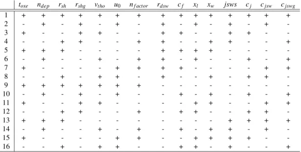
As show in Table 4, 15 different BSIM4 parameters have been screened out. DC and AC simulation is performed on single transistor. With Plackett Burman design (see Table 4), Table 5 and 6 illustrates the result of stepwise regression analysis with F-statistical model with entrance and exit tolerances p value 0.05 and 0.1 separately (default values). The impact degree of process variation to performance is sorted by serial numbers, where vthoand xlhave the highest impact on circuit performance. Consideration should also be given to process
parameters such as u0, xw, ndepand toxe.
Figure 15 illustrates the statistical design flow aware process variation. Detail algorithms is shown in Algo-rithm 1. The flow has been applied to an op-amp in folded cascade architecture. The circumscribed type central
toxe ndep rsh rshg vtho u0 nf actor rdsw cf xl xw jsws cj cjsw cjswg 1 + + + + + + + + + + + + + + + 2 - + - + - + - + - + - + - + -3 + - - + + - - + + - - + + - -4 - - + + - - + + - - + + - - + 5 + + + - - - - + + + + - - - -6 - + - - + - + + - + - - + - + 7 + - - - - + + + + - - - - + + 8 - - + - + + - + - - + - + + -9 + + + + + + + - - - -10 - + - + - + - - + - + - + - + 11 + - - + + - - - - + + - - + + 12 - - + + - - + - + + - - + + -13 + + + - - - + + + + 14 - + - - + - + - + - + + - + -15 + - - - - + + - - + + + + - -16 - - + - + + - - + + - + - - +
toxe: Electrical gate equivalent oxide thickness
ndep: Channel doping concentration at depletion edge for zero body bias
rsh: Source/drain sheet resistance
rshg: Gate electrode sheet resistance
vtho: Threshold voltage at vbs=0 for long-channel devices
u0: Low-field surface mobility at tnom
nf actor: Subthreshold swing coefficient
rdsw: Zero bias LDD resistance per unit width for RDSMOD=0
cf: Fringing field capacitance
xl: Length variation due to masking and etching
xw: Width variation due to masking and etching
jsws: Isolation-edge sidewall source junction reverse saturation current density cj: Zero bias bottom junction capacitance per unit area.
cjsw: Sidewall junction capacitance per unit periphery.
cjswg: Gate-side junction capacitance per unit width.
Table 4: Plackett Burman design: 15 two-level factors for 16 runs with BSIM4 parameters
1 2 3 4 5 6 7 8
Id xl vtho u0 xw toxe rdsw ndep
Vth vtho xl ndep toxe xw rdsw rsh cf
gm u0 xl rdsw xw vtho toxe toxe
Table 5: BSIM4 parameters selection: DC simulation
1 2 3 4
A0 vtho xl u0 cjswg
GBW xl vtho u0 toxe
Figure 15: Statistical design flow aware process variation
composite design allocates the response distribution of process parameter. Figure 16 shows the response surface modeling from BSIM4 parameters Vth0(threshold voltage variation) and Xl(length variation) to circuit
perfor-mance DC gain. We can evaluate the perforperfor-mance distribution according to process variation. This methodology can be extended to high system level to predict the system performance and calculate yield.
0.18 0.2 0.22 0.24 0.26 0.28 0.3 0 0.2 0.4 0.6 0.8 1 x 10⁻⁸ −200 −100 0 100 length variation Vth0 A0 −100 −80 −60 −40 −20 0 20 40 60 Simulation Data Response Surface
4
Conclusions
Reliability-aware integrated circuit design is a topic involving many aspects. Methodologies such as hierarchy-behavioral modeling should be developed for mixed-signal circuits. It has been demonstrated on a low power second order CTΣ∆ modulator with CMOS 65 nanometer technology. A comprehensive assessment for reliabil-ity mechanism HCI and NBTI is performed at transistor level. It is confirmed that NBTI is the dominate effect in this CTΣ∆ modulator. From behavioral simulation at system level, we conclude that in low order CT Σ∆ modulator, feedback loop is less reliable than analog loop filter. Weak spot detection and circuit overdesign are also implemented. It is indicated that DAC is the most sensitive building block inΣ∆ modulator.
It should be mentioned that the Monte-Carlo simulation remains the most realistic methodology when esti-mating the process variation. Statistical methodology can achieve better efficiency than Monte-Carlo simulation, with the loss of accuracy. Statistical design is also involved with hierarchy-behavioral modeling methodology. We use the DoE-RSM flow to consider process variation in BSIM4 transistor model. The quadratic response surface can estimate the system performance and yield information.
5
Perspective and future work
More and more work on IC reliability issues have been published in the year of 2010 and 2011. Our survey shows that researchers are looking at and dealing with transistor reliability and variability issues at 32 nanometer and below. Therefore, methodologies should be compatible with different CMOS technology. For analog and mixed-signal systems, 65 nanometer CMOS technology is still playing an important role in IC manufacturing. On the other hand, we need to develop methodologies with easy approach for circuit designers. The reliability and variability aware methodologies could be applied to IC systems as many as possible.
The further work will continues to focus on reliability issue of reconfigurable low orderΣ∆ modulators, such as feedback strategy changing (NRZ feedback) and architecture alteration (CIFF, CRFB). For behavioral modeling, [29] introduces a method to characterize sampling aperture of clocked comparators, it offers us the reference in behavioral modeling of quantizer with extra degrees. Based on current research work, we need to combine ageing effects and process variations and evaluate the circuit performance degradation in design phase. Besides HCI and NBTI effect, other degradation mechanisms like TDDB should be included.
References
[1] “International technology roadmap for semiconductors(ITRS)[online],” 2009. [Online]. Available: www.itrs.net/Links/2009ITRS/Home2009.htm
[2] H. Cai, H. Petit, and J.-F. Naviner, “A hierarchical reliability simulation methodology for ams integrated circuits and systems,” Journal of Low Power Electronics, vol. 8, no. 5, pp. 697–705, 2012.
[3] G. Gielen, P. D. Wit, E. Maricau, J. Loeckx, J. Martin-Martinez, B. Kaczer, G. Groeseneken, R. Rodriguez, and M. Nafria, “Emerging yield and reliability challenges in nanometer cmos technologies,” Proc. Design, Automation and Test, 2008.
[4] W. Wang, “Circuit aging in scaled CMOS design:modeling,simumation,and prediction,” Ph.D disserta-tion,Arizona State University, 2008.
[5] R. Vattikonda, W. Wang, and Y. Cao, “Modeling and minimization of PMOS NBTI effect for robust nanometer design,” IEEE/ACM Design Automation Conference, pp. 1047–1052, 2006.
[6] E. Maricau and G. Gielen, “Transistor aging-induced degradation of analog circuits: Impact analysis and design guidelines,” pp. 243–246, sept. 2011.
[7] W. Wang, V. Reddy, R. Vattikonda, S. Krishnan, and Y. Cao, “Compact modeling and simulation of circuit reliability for 65nm CMOS technology,” Measurement, 2007.
[8] S. V. Kumar, C. H. Kim, and S. S. Sapatnekar, “An analytical model for negative bias temperature instabil-ity,” Proc.Int.Conf.Comput.-Aided, pp. 493–496, 2006.
[9] Paul.B.C, K.Kang, Kufluoglu.H, Ashraful.Alam.M, and Roy.K, “Temporal performance degradation under NBTI: Estimation and design for improved reliability of nanoscale circuits,” Proc.ACM/IEEE Des.Autom.Test Eur., pp. 780–785, 2006.
[10] J. W. McPherson, “Reliability challenges for 45nm and beyond,” Proc.ACM/IEEE Des.Autom.Test Eur., pp. 176–181, 2006.
[11] P. M. Ferreira, H. Petit, and J. Naviner, “AMS and RF design for reliability methodology,” Proc.ISCAS/IEEE Int.Sym. on Cir. and Sys., pp. 3657–3660, 2010.
[12] J. H. Stathis, “Percolation models for gate oxide breakdown,” J. Appl.Phys., vol. 86, no. 10, pp. 5757–5766, 1999.
[13] J. Lienig, “introduction to electromigration-aware physical design,” Proc. int. symposium on Physical de-sign, 2006.
[14] H. Cai, H. Petit, and J.-F. Naviner, “Reliability analysis of continuous-time sigma-delta modulator,” Euro-pean Sym. on Reliability of Electron Devices, Failure Physics and Analysis, October 2011.
[15] C. Hu, “IC reliability simulation,” IEEE Journal of Solid-State Circuits, vol. 27, no. 3, pp. 241–246, 1992. [16] X. Xuan, A. Chatterjee, A. Singh, N. Kim, and M. Chisa, “IC reliability simulator ARET and its application
in design-for-reliability,” Proc. ATS, pp. 18–21, 2003.
[17] C. Bestory, F. Marc, and H. Levi, “Multi-level modeling of hot carrier injection for reliability simulation using vhdl-ams,” Forum on specification and design language, 2006.
[18] H. Cai, H. Petit, and J.-F. Naviner, “Reliability aware design of low power continuous-time sigma-delta modulator,” Microelectronics reliability journal, vol. 51, no. 9-11, pp. 1449–1453, December 2011. [19] V. Veetil, D. Sylvester, and D. Blaauw, “Efficient monte carlo based incremental statistical timing analysis,”
Proc. of IEEE/ACM on Design Automation Conference, pp. 676–681, 2008.
[20] J. Jaffari and M. Anis, “On efficient monte carlo-based statistical static timing analysis of digital circuits,” Proc. of IEEE/ACM on Computer-Aided Design, ICCAD, pp. 196–203, 2008.
[21] J. Kim, K. D. Jones, and M. A. Horowitz, “Fast, non-monte-carlo estimation of transient performance variation due to device mismatch,” Proc. of IEEE/ACM on DAC, pp. 440–443, 2007.
[22] G. Gielen, “Design tool solutions for mixed-signal RF circuit design in CMOS nanometer technologies,” Proc. Design, ASP Des.Auto.Conf., pp. 432–437, 2007.
[23] M. Pelgrom, A. Duinmaijer, and A. Welbers, “Matching properties of MOS transistor,” IEEE J.Solid-state Circuits, vol. 24, no. 5, pp. 1433–1440, 1989.
[24] C. Forzan and D. Pandini, “Statistical static timing analysis: a survey,” Integration,the VLSI journal 42, pp. 409–435, 2009.
[25] H. Tang, “Hierarchical statistical analysis of performance variation for continuous-time delta-sigma modu-lators,” Proc. of International Conf. on VLSI SOC, pp. 37–41, 2007.
[26] G. Yu and P. Li, “Lookup table based simulation and statistical modeling of sigma-delta ADCs,” Proc. of IEEE/ACM on Design Automation Conference, pp. 1035–1040, 2006.
[27] R. Plackett and J. Burman, “The design of optimum multifactorial experiments,” Biometrika, vol. 33, no. 4, pp. 305–325, June 1946.
[28] Mathworks, “Matlab, version 2010.”
[29] M. Jeeradit, J. Kim, B. Leibowitz, P. Nikaeen, V. Wang, B. Garlepp, and C. Werner, “Characterizing sam-pling aperture of clocked comparators,” pp. 68 –69, june 2008.