DURABLE THERMOCHROMIC VO2 FILMS DEPOSITED BY HIPIMS
SIMON LOQUAI
DÉPARTEMENT DE GÉNIE PHYSIQUE ÉCOLE POLYTECHNIQUE DE MONTRÉAL
THÈSE PRÉSENTÉE EN VUE DE L’OBTENTION DU DIPLÔME DE PHILOSOPHIAE DOCTOR
(GÉNIE PHYSIQUE) FÉVRIER 2017
ÉCOLE POLYTECHNIQUE DE MONTRÉAL
Cette thèse intitulée:
DURABLE THERMOCHROMIC VO2 FILMS DEPOSITED BY HIPIMS
présentée par : LOQUAI Simon
en vue de l’obtention du diplôme de : Philosophiae Doctor a été dûment acceptée par le jury d’examen constitué de :
M. PETER Yves-Alain, D. Sc., président
M. MARTINU Ludvik, Ph. D., membre et directeur de recherche
Mme KLEMBERG-SAPIEHA Jolanta-Ewa, Doctorat, membre et codirectrice de recherche M. WERTHEIMER Michael R., D. Sc. A., membre
DEDICATION
ACKNOLEDGEMENTS
First, I would like to thank both of my advisors, Ludvik Martinu and Jolanta-Ewa Klemberg-Sapieha, who support and direct me for all those years. Under their supervision, I grow as from an engineer to a scientist.
Second, I would also like to thank Michael Wertheimer, Prof Ulf Helmersson and Prof Yves-Alain Peter for their acceptance to read my dissertation and to be my jury members. I would like to thank Margaret McKyes for the English editing on some part of this thesis.
Therefore, I would like to thank Oleg Zabeida for his expertise in plasma and vacuum systems, and Bill Baloukas for his expertise in active optical materials. Their combined expertise allows me to overcome many hurdles and motivates me during down times in this project.
The Functional Coating and Surface Engineering Laboratory (FCSEL) will be nothing without the technical assistance of both Francis Turcot and Sébastien Chénard. Your hard work and efficiency keep the system running and our research active.
I would like to personally thank Matjaz Panjan for taking me under his wing during this few months in 2013. I learned a lot with you, especially how to plan an experiment and get things done when its running.
I would like to thank the summer students that work with me during those last seven years, Aimé Labbé, Philippe Jubinville and Rodrigue Beaini.
I would like not to forget all my colleagues at the FCSEL, who are excellent scientists and eventually became good friends: Alexis Ragusish, Amaury Kilicaslan, Erika Herrera, Fabrice Pougoum, Francis Blanchard, Gabriel Taillon, Jacques Lengaigne, Jean-Phillipe Fortier, Jincheng Qian, Jiri Capek, Jiri Kohout, Julien Gagnon, Julien Schmitt, Martin Caron, Matej Hala, Médard Koshigan, Michael Laberge, Soroush Hafezian, Stephen Brown, Thomas Poirié, Thomas Schmitt, William Trottier, Yuxiao Wu, and all the former students.
Finally, I would like to thank my family and my fiancé Aurélie for supporting me during all those years.
RÉSUMÉ
Le dioxyde de vanadium, VO2, est le matériau thermochromique le plus étudié. Il présente une transmission de la lumière infrarouge élevée à basse température et une extinction de cette dernière au-dessus de sa température critique. Ce changement de propriété est réversible et ne nécessite pas de stimulus externe. De ce fait, le VO2 est un candidat parfait pour les applications de contrôle de transfert d’énergie. L’application la plus directe est celle des vitrages dits ‘intelligents’, où la couche mince thermochromique module la transmission du rayonnement solaire infrarouge en fonction de la température. Un tel dispositif contrôle la température du milieu ambiant passivement, limitant la consommation des équipements de chauffage et climatisation. Dans un objectif similaire, les matériaux thermochromiques peuvent aussi être utilisés pour créer des dissipateurs thermiques pour les satellites, appelés ‘Smart Radiative Device’ (SRD). Cependant, les dispositifs thermochromiques à base de VO2 sont toujours à l’échelle du laboratoire, principalement à cause de la complexité de synthèse du VO2. Le Vanadium est en effet un métal de transition, possédant de multiple oxydes stœchiométriques dont seul le VO2 présente un intérêt pour ces applications. Un contrôle du niveau d’oxydation lors du dépôt est donc nécessaire, complexifiant l’industrialisation du procédé. De plus, la température de dépôt du matériau pour obtenir la phase cristalline, généralement 400°C, génère un cout prohibitif pour beaucoup d’industriels.
Lors de la dernière décade, la communauté scientifique des dépôts physiques en phase vapeur a connu une forte effervescence autour d’une nouvelle technique, la pulvérisation magnétron pulsée de haute puissance (HiPIMS en anglais). Cette dernière combine la flexibilité des procédés de pulvérisation magnétron avec la modulation du temps d’impulsion pour obtenir un plasma de haute densité. Cette technologie est prometteuse pour le dépôt de couches minces. En particulier en mode réactif, le procédé HiPIMS offre un taux de dépôt avantageux comparé au procédé conventionnel de pulvérisations; tout en améliorant les propriétés des couches déposées, telles qu’une plus haute densité, une contrainte mécanique inférieure et un abaissement de la température nécessaire pour obtenir des couches minces cristallines. Les contributions des différents effets de la décharge HiPIMS (haut flux d’ions de basse énergie et le rayonnement du plasma) à la performance des couches ne sont pas encore expliquées, malgré une bonne connaissance du comportement de la décharge HiPIMS. De ce fait, nous avons choisi d’appliquer ce procédé au dépôt de couches minces de VO2 afin d’en améliorer les propriétés et illustrer les aventages du procédé HiPIMS pour le dépôt de ce type d’oxyde.
En premier, nous avons observé l’expansion du plasma réactif HiPIMS au-dessus d’une cible métallique de vanadium. Cette mesure se fait à l’aide d’une caméra haute vitesse et de filtres interférentiels passe-bande permettant de séparer les différentes plages énergétiques de l’émission optique du plasma. Il a été démontré que la décharge HiPIMS opérée dans un mélange argon-oxygène a des caractéristiques très similaires aux décharges dans des atmosphères d’argon et d’oxygène pour la période allumée du pulse. Cependant, dans les premières microsecondes après l’extinction du plasma, la post-décharge, une forte émission optique est observée pour les espèces de faible énergie du plasma. Ce phénomène d’émission optique est lié au refroidissement des électrons une fois que le voltage appliqué à la cathode est supprimé, suivi de la diffusion de ces électrons dans le champ magnétique jusqu’au point d’annulation du champ (piège magnétique). Ce phénomène optique nécessite un seuil d’oxygène inséré dans la chambre, nous avons supposé que les électrons refroidis interagissent avec les molécules d’oxygène sous forme d’une réaction de capture dissociative. Les ions négatifs créés par cette réaction peuvent ensuite se recombiner avec les ions positifs environnants, peuplant les niveaux radiatifs observés lors de l’imagerie haute vitesse. Les espèces recombinées possèdent aussi une énergie cinétique estimée à près de 1 eV, ce qui génère un bombardement ionique de faible énergie de la couche mince en croissance. En conclusion, cet effet présent dans les décharges pulsées offre une source d’oxygène atomique supplémentaire et explique partiellement la réactivité plus grande des décharge HiPIMS, diminuant le flux d’oxygène nécessaire pour déposer des oxydes stœchiométriques. De plus, le flux de particules fournit une partie de l’énergie nécessaire pour abaisser la température de dépôt de ces oxydes sous forme de couches cristallines.
Nous avons ensuite cherché à démontrer l’intérêt de l’abaissement de la température de dépôt de VO2 à l’aide de substrat polymère. En utilisant l’énergie apportée par le procédé HiPIMS, des couches minces de VO2 ont été synthétisées sur deux type de polyimides: le Kapton HN et le Kapton CS. Le Kapton HN est un standard de l’industrie aérospatiale, un polymère orange à haute résistance thermique et connu pour survivre dans le vide spatial. Au contraire, le Kapton CS est un polymère transparent de résistance thermique inférieure mais d’intérêt pour les applications de fenêtres intelligentes. Les couches minces déposées sont thermochromiques, avec des changements de propriétés optiques attendues dans l’infrarouge, une première pour du VO2 déposé sur un substrat polymère. La stœchiométrie du matériau a été confirmée par mesure de spectroscopie photoélectronique X (XPS). Cependant, la nature des polymères utilisés rend impossible de
confirmer la structure cristalline directement; celle-ci fut mesurée par diffraction des rayons X (XRD) et spectroscopie Raman sur des substrats de silicium insérés dans la chambre lors des dépôts sur Kapton. Ces mesures présentent des spectres comparables avec la littérature. La composition des couches minces a pu être calculée à l’aide des spectroscopies de rétrodiffusion de Rutherford (RBS) et détection de recul élastique (ERD). Ces résultats concordent avec les mesures XPS, tout en soulevant la présence de diffusion du vanadium dans le substrat polymère. Cette diffusion d’atomes améliore l’adhésion des couches minces au détriment d’une perte sèche de vanadium. Une diffusion similaire a été observée sur les échantillons déposés sur des substrats de verres, avec la présence de bore au sein de la couche de VO2.
La dernière étude cherche à contrôler la diffusion à l’aide d’une barrière à l’interface VO2/verre. Le VO2 se dégradant fortement en milieu humide, une seconde barrière de diffusion est envisagée à la surface des échantillons. Le matériau choisi est le nitrure de silicium, SiNx, connu pour ses bonnes propriétés de barrière de diffusion ainsi que pour sa stabilité à haute température; de plus, ce matériau est simple à déposer par pulvérisation magnétron. Pour estimer la durabilité des couches de VO2, des échantillons de références sont déposés à l’aide de la méthode conventionnelle de pulvérisation magnétron radiofréquence (RFMS). Avant exposition à un environnement humide, les échantillons présentent des propriétés optiques similaires et ne peuvent pas être différenciés formellement par Raman et XRD. L’utilisation d’une barrière de diffusion SiNx est un succès, aucune dégradation majeure n’étant observée sur les couches protégées, tout comme une absence de diffusion du bore dans le VO2. Au contraire, pour les couches où le VO2 est exposé à l’environnement oxydant, une différence marquante entre les couches préparées par HiPIMS et RFMS est obtenue. Alors que les échantillons préparés par RFMS se dégradent très rapidement, les échantillons préparés par HiPIMS offrent une période d’incubation où la dégradation des propriétés optiques est très lente. L’analyse d’image de microscopie électronique à balayage et de la densité des couches minces par RBS-ERD montre que les couches HiPIMS incorporent moins d’hydrogène lors de la dégradation. De plus, il ne se forme pas les aiguilles poreuses en surface observées sur les couches RFMS. Nous lions cet effet à une plus grande densité des grains de la couche, qui limite la diffusion de l’oxygène lors de la dégradation et donc ralentit le phénomène de dégradation.
ABSTRACT
Vanadium dioxide, VO2, is a well-known thermochromic material that exhibits high or low infrared transmittance when its temperature is below or above a critical temperature, respectively. Because this change in properties is reversible, VO2 has long been a candidate for radiative energy control devices. One innovative application is the smart window, in which a thermochromic layer controls the transmission of infrared radiation from the sun as a function of the surrounding temperature. This enables self-controlled temperature regulation, which in turn limits heating and cooling requirements. Similar devices called smart radiator devices (SRDs) are being developed for passive cooling of satellites. However, all these applications remain in the development phase due to VO2 deposition issues. Vanadium is a transition metal that exhibits multiple oxide stoichiometries, of which only VO2 is of interest. Precise control of the oxygen fraction is therefore needed for VO2 synthesis, accompanied by a high deposition temperature, usually around or in excess of 400 °C, in order to obtain the crystalline material. These imperatives currently limit industrial applications of VO2.
Over the past decade, high power impulse magnetron sputtering (HiPIMS) has emerged as a newcomer in the magnetron sputtering community. Because HiPIMS combines the versatility of magnetron sputtering with short high power pulses to generate highly ionized plasma, it is a promising technique for thin film material deposition. In reactive sputtering, HiPIMS provides deposition rates similar to or higher than those for conventional sputtering, along with superior film properties such as higher density and lower stress, among others. Furthermore, crystalline films can be obtained at lower deposition temperature. However, the impacts of the high ion flux, plasma radiation, and HiPIMS dynamics on the metal-oxide properties are still unclear, despite a good understanding of the HiPIMS discharge. We therefore chose to apply HiPIMS to thermochromic VO2 to demonstrate the advantages of using HiPIMS to deposit crystalline films.
First, the expansion of a reactive-HiPIMS discharge over a vanadium target was investigated using high-speed plasma imaging combined with optical bandpass filtering. The results showed that the reactive discharge operating in an argon–oxygen mixture behaved similarly in “pulse-on” time to discharges in pure argon and oxygen. However, in the post-discharge, the first microsecond after the cathode voltage was removed, strong light emission in the low-energy spectra was observed. This light emission can be explained by electrons that cool and drift toward the null magnetic field
trap. A threshold oxygen content in the mixture is needed in order to observe this phenomenon. This led us to hypothesize that the main interaction is dissociative attachment between the electrons and the molecular oxygen. The resulting negative ions recombine with positive ions, generating excited radiative species. These resulting species, which have an estimated kinetic energy approaching 1 eV, provide a low-energy bombardment of the growing films. This reaction in pulsed plasma also generates additional atomic oxygen, compared to conventional magnetron sputtering. Therefore, such post-discharge emission provides a partial explanation for the reactivity observed in the pulsed discharge, for the lower oxygen content needed to produce stoichiometric material, and for the lower temperature required to deposit crystalline films.
Following the exploration of the reactive discharge, HiPIMS, a previously demonstrated approach to lower the deposition temperature, was used to deposit thermochromic VO2 on polymer substrates. Using the energetic HiPIMS process, VO2 films were synthesized onto two different polyimide substrates, Kapton® HN and Kapton® CS. These two substrates present different optical properties that target different potential applications of VO2 for energy-control devices. First, Kapton® HN, an orange-tinted polymer, is standard in the aerospace industry because it is resistant to high temperatures and space radiation. On the other hand, Kapton® CS provides a clear substrate with moderate temperature resistance, and is more suitable for earthbound applications such as smart windows. The produced films exhibited active thermochromic behavior, the first time that this has been achieved with VO2 on a polymer substrate. The film stoichiometries were confirmed by X-ray photoelectron spectroscopy (XPS). Unfortunately, due to the nature of the polymer substrate, it was not possible to directly quantify the film crystallinity. However, Raman spectroscopy and X-ray diffraction (XRD) of the deposits on silicon strips showed spectra comparable to those in the literature. Rutherford backscattering spectrometry (RBS) and elastic recoil detection (ERD) were used to confirm the stoichiometric composition of the Kapton®-coated sample, revealing a strong need for film–substrate interface control. In fact, pronounced diffusion of vanadium and oxygen into the polymer substrate was measured. Although this diffusion could improve the film adhesion, it represents a net loss of material in terms of deposition efficiency. Similar diffusion was observed for reference films deposited onto glass substrates; namely vanadium diffusion into glass, and boron (glass dopant) diffusion into VO2.
To prevent this type of diffusion at the VO2–glass interface, the design was improved with the addition of a barrier coating. Because it is well known that thermochromic VO2 is sensitive to water
degradation, an additional diffusion barrier was added as a top layer. For this purpose, we chose SiNx, a commonly used diffusion barrier that is stable at high temperatures and can be deposited by magnetron sputtering. To assess film durability, VO2 films were deposited using both HiPIMS and conventional RFMS. Before oxidation, the deposited devices presented similar transmission and performance in terms of infrared modulation, independently of the deposition method. Raman and XRD were unable to detect significant differences in the HiPIMS- and RFMS-deposited VO2. As expected, SiNx provided an adequate diffusion inhibiter. No trace of the glass dopant was found in the VO2 layers, and both RFMS- and HiPIMS-deposited coatings provided good resistance to a steam environment. However, the unprotected VO2 coating behaved differently. The HiPIMS-deposited layers exhibited slower kinetics, with an incubation period of slow degradation, whereas the RFMS-deposited VO2 layer showed rapid dissolution. Based on the results of scanning electron microscopy (SEM) image analysis combined with RBS/ERD density measurement, we attributed the higher durability of the HiPIMS-deposited VO2 coating to a higher grain density, low amount of grain boundaries, which lowered oxygen diffusion at grain boundaries and hence slowed the material degradation. On the other hand, the lower density of the RFMS-deposited layer gave rise to high roughness, with V2O5 needles topping the SiNx layer. The higher diffusion of atoms into the RFMS sample was confirmed by the ERD-measured hydrogen content, showing higher hydrogen density in the vanadium layer during water oxidation in the RFMS-deposited layers.
TABLE OF CONTENTS
DEDICATION ... iii ACKNOLEDGEMENTS ... iv RÉSUMÉ ... v ABSTRACT ... viii TABLE OF CONTENTS ... xi LIST OF TABLES ... xvLIST OF FIGURES ... xvi
LIST OF SYMBOLS AND ACRONYMS ... xxv
CHAPTER 1 INTRODUCTION ... 1
Objectives ... 7
Publications ... 8
Outline of the thesis ... 10
CHAPTER 2 THEORETICAL BACKGROUND, VO2 ... 11
Foreword ... 11
Vanadium oxides ... 11
VO2 phase transition ... 14
VO2 coating index of performances ... 19
Polycrystalline VO2 ... 20
Process functionalization of VO2 ... 21
Functionalization of VO2 devices ... 26
CHAPTER 3 THEORETICAL BACKGROUND, PLASMA AND MAGNETRON
SPUTTERING ... 37
Foreword ... 37
General plasma properties ... 37
Ion-Surface interaction ... 42
Thin film growth ... 46
Magnetron sputtering and HiPIMS ... 49
CHAPTER 4 EXPERIMENTAL METHODOLOGY ... 57
Deposition systems ... 57
4.1.1 Power Supplies ... 57
4.1.2 Deposition Chambers ... 59
Optical emission spectroscopy ... 62
4.2.1 Principle of atomic line emission ... 63
4.2.2 Experimental apparatus ... 66
Film characterization technique ... 69
4.3.1 Spectrophotometry ... 69
4.3.2 Spectroscopic ellipsometry ... 69
4.3.3 Rutherford backscattering spectroscopy and elastic recoil detection. ... 73
CHAPTER 5 ARTICLE 1: FLASH POST-DISCHARGE EMISSION IN A REACTIVE HIPIMS PROCESS ... 76
Introduction ... 77
Experimental Methodology ... 77
Results and discussion ... 78
CHAPTER 6 ARTICLE 2: HIPIMS-DEPOSITED THERMOCHROMIC VO2 FILMS ON
POLYMERIC SUBSTRATES ... 87
Introduction ... 88
Experimental methodology ... 90
6.2.1 Substrates and deposition process ... 90
6.2.2 Film characterization ... 92
Results and Discussion ... 95
6.3.1 HiPIMS deposition and process optimization ... 95
6.3.2 Thermochromic properties of the VO2 films on polymer substrates ... 99
6.3.3 Ellipsometry measurements and the optical properties ... 105
6.3.4 Composition and microstructure ... 107
Conclusions ... 114
CHAPTER 7 ARTICLE 3: HIPIMS-DEPOSITED THERMOCHROMIC VO2 FILMS WITH HIGH ENVIRONMENTAL STABILITY ... 117
Introduction ... 118
Methodology ... 120
7.2.1 Film deposition ... 120
7.2.2 Film ageing and characterization ... 121
Results and discussion ... 124
7.3.1 Optical properties ... 124
7.3.2 Microstructural characteristics ... 129
7.3.3 Effect of a SiNx top barrier coating ... 136
Conclusion ... 137
CHAPTER 8 GENERAL DISCUSSION, CONCLUSIONS AND PERSPECTIVES ... 139
Thermochromic VO2 by HiPIMS ... 142
Perspectives and future work ... 146
8.3.1 Discharge characterization ... 146
8.3.2 Toward solar gain control in smart windows ... 147
8.3.3 Passive radiator control ... 148
8.3.4 Concluding Remarks ... 150
LIST OF TABLES
Table 1-1 Performance indexes for various chromogenic smartwindows. Tlum is the visible light transmittance, Tsol is the fraction of solar radiation transmittance. Index calculation methods
are given in Chapter 2. ... 5
Table 1-2 List of articles related to this Ph.D. thesis. ... 8
Table 1-3 List of articles resulting from collaborations. ... 9
Table 1-4 List of contributions to international conferences. ... 9
Table 2-1 Known critical transition temperature and formation enthalpy of vanadium oxides. ... 13
Table 2-2 Cell parameters of monoclinic and tetragonal VO2 phases. ... 13
Table 3-1 Atomic Mass and binding energy of various interesting metals for sputtering, from [132]. ... 45
Table 4-1 Technical data of the three HiPIMS pulsers used for this thesis ... 60
Table 4-2 Spectrometers characteristics ... 68
Table 6-1 Deposition parameters for thermochromic VO2 films and TiO2 seed layers. ... 92
Table 6-2 List of studied samples and the respective VO2 deposition temperatures. * denotes the expected thickness. ... 94
Table 6-3 Atomic composition obtained by XPS before and after ion cleaning. ... 109
Table 6-4 Average composition obtained from ToF-ERD measurements of the grey zone shown in Figure 6-10. ... 112
Table 7-1 Deposition parameters for VO2 and SiNx films ... 121
Table 7-2 EDS results for regions A and B (see Figure 7-6) of a RFMS-deposited VO2 sample aged for 52 hours. ... 134
Table 8-1 Characteristics of the different pulses used to deposit thermochromic VO2 and optimal oxygen flow rates. ... 143
LIST OF FIGURES
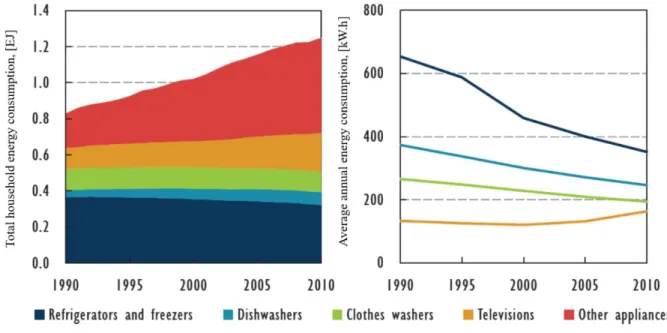
Figure 1-1 Large and small appliance energy consumption in the Organization for Economic Co-operation and Development (OECD) countries for the last two decades. Left panel presents the total consumption by appliances; right panel presents the average consumption for each unit. Reproduced from [7]. ... 2 Figure 1-2 Global building final energy use fuel shares for residential and services, 2012. Final
energy refers to the energy delivered to the building, not how it is used in the building. For example, natural gas denotes that the building uses a system that burns natural gas, to generate either heat or electricity. Reproduced from [6]. ... 3 Figure 1-3 Normalized solar energy spectrum at sea level ASTM-G173-03 (grey) and optimal
window energy transmittance (green). ... 4 Figure 2-1 The O-V phase diagram (reproduced from [19] with permission of Springer). ... 12 Figure 2-2 Structure diagram of thermochromic VO2 crystal cells. The left panel shows the low
temperature insulator monoclinic cell while the right panel shows the high temperature conductive tetragonal cell (adapted from [27]). ... 14 Figure 2-3 Illustration of the VO2 band structure. The left portion presents the low temperature
monoclinic insulator state, with a split V3d|| that creates an indirect band gap of 0.65 eV, and a direct band gap of 0.65 eV; the right portion presents the tetragonal conductive state, where the non-degenerate V3d|| band overlaps the V3dπ* band to form a metal-like conductive state (adapted from [17]). ... 15 Figure 2-4 Optical parameters n and k at low and high temperature states of thermochromic VO2
(reproduced from [44] with permission from Elsevier). ... 18 Figure 2-5 Variation of the transmission spectra for a VO2 thin film at low and high temperature
phases. The grey shade represents the solar irradiance as defined by the ASTM G173-03 [48]. ... 19 Figure 2-6 Effect of the underlying TiO2 crystal film orientation on the VO2 phase transition in
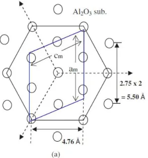
Figure 2-7 Schematics of the 0001 plane of the Al2O3 hexagonal crystal structure (open circle) and the thermochromic VO2 M1 monoclinic 010 cell (Blue). cm and am are the VO2 crystallographic structure cell as shown in Table 2-2 (adapted from [56]). ... 23 Figure 2-8 Effect of substrate temperature on the performance of VO2 thins film deposited on a
crystalline Al2O3 substrate (a) (adapted from [60], copyright 1997 American Vacuum Society), and glass substrate (b) (adapted from [44] with permission from Elsevier). ... 24 Figure 2-9 Effect of doping on the phase transition of VO2 thin films in the case of W-doping on
the resistivity (a) (adapted from [59] with the permission of AIP Publishing), or co-doping W and F on ΔT2500 nm (b) (adapted from [67] with permission from Elsevier). ... 25 Figure 2-10 Spectral transmission of a VO2 film sandwiched between two TiO2 layers on SiO2,
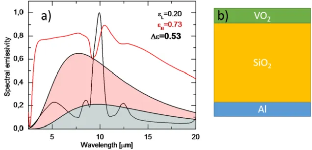
with an increased visible transmittance over a similar single layer of VO2 deposited on the same substrate (adapted from [81] with permission of Springer). ... 26 Figure 2-11 Spectral emissivity of an optimized VO2/SiO2/Al thermochromic stack at low (black)
and high temperature (red) (a) and a schematic of the modelled device (b). Calculated using an approach from [97]. ... 28 Figure 2-12 (a) Electrical resistivity of multi-stacked W-doped VO2 layers, heating (open circles)
and cooling cycles (closed circles) with a linear model (1) (open squares for heating cycle and closed squares for cooling cycle). (b) Derivative plot of the temperature-dependent resistivity fitted with Gaussian to obtain the individual transition temperature of each layer (reproduced from [59] with the permission of AIP Publishing). ... 29 Figure 2-13 Refractive indices (a) and micro-hardness (b) of various functional coatings and
substrates (reprinted from [101] with permission from Elsevier). ... 30 Figure 2-14 Schematic of a PLD chamber, and dynamics of the plasma plume during the PLD
process (adapted from [102]). ... 31 Figure 2-15 Schematic views of typical CVD process chambers. Cold wall reactors (a, b), hot wall
reactor (c) and barrel reactor (d) (reprinted from [107] with permission from Elsevier). ... 32 Figure 2-16 Specular spectral transmittance of 80 µm VO2 doped polysiloxane films at different
Figure 2-17 Deposition rate, discharge voltage and deposited phases of vanadium oxides by direct current magnetron sputtering at a constant power of 200 W. One can observe a hysteresis in the discharge voltage due to the choice of direct current magnetron sputtering, DCMS (reproduced from [118] with permission from Elsevier) ... 35 Figure 3-1 Schematics of a vacuum glow discharge with the electrons, ions and neutrals in the
quasi-neutral bulk plasma. ... 39 Figure 3-2 Secondary electron emission coefficients for Ar and Ar+ on clean and contaminated
metal surfaces from the model proposed by Phelps in [128]. The experimental data used to build the model present a small impact of the metal atomic number (adapted from [20]). ... 42 Figure 3-3 Schematics of the various plasma energetic particle surface interactions (reproduced
from [129] Copyright 1989 American Vacuum Society)... 44 Figure 3-4 Sputtering Yield of Ar+ ions on a clean vanadium surface as a function of the ion energy
(reproduced from [132]). ... 45 Figure 3-5 Structure Zone Diagram with generalized growth temperature and normalized energy,
T* represents the reduced temperature and E* represents the energy per deposited atoms (reproduced from [138] with permission from Elsevier). ... 47 Figure 3-6 Plot of the ions/neutral flux ratio versus the average ion energy for the growth of
structurally modified films with a high density for Si3N4:H (A), SiO2:H (B), a-C:H (C), and TiO2 (D, E) obtained from microwave and radiofrequency PECVD. Other materials deposited by PVD are reported: SiO2 (circles), dielectrics (triangle), metals (square), semiconductors (lozenges). It shows that an below average energy per deposited atom of 1 eV/atom, no effect of the bombardment is obtained, while above 100 eV/atom, film growth is compromised up to the point of total sputtering of the growing film (reprinted from [101] with permission from Elsevier). ... 48 Figure 3-7 Magnetic field map of the extremely unbalanced magnetron. The magnets are placed
on the left, at the 0 position and the central red zone is the null-magnetic zone. ... 49 Figure 3-8 Graphical representation of the classification of magnetron sputtering process as a
of the plasma density is obtained through an increase of the instantaneous power (reproduced from [142] copyright 2012 American Vacuum Society). ... 50 Figure 3-9 Optical emission intensities from discharges operated by HiPIMS, MPPMS and DCMS
above a Nb target in pure Ar (a) and in O2/Ar mixture (b), normalized with an average power of P = 320W. The intensities were multiplyed to clarify (reproduced from [143] © IOP Publishing. Reproduced with permission. All rights reserved). ... 51 Figure 3-10 Distribution of the electron energy in the HiPIMS at various times during the 100 µs
pulse, showing the high-energy electrons produced in the first 10 µs. These measurements were performed at 0.5 Pa with a peak power density of 500 W.cm-2 over a Ti target in pure Ar atmosphere (reproduced from [155] © IOP Publishing. Reproduced with permission. All rights reserved). ... 52 Figure 3-11 Mass spectra at 2 eV of positive (a) and negative (b) ions generated in reactive HiPIMS
over a Ti target in an 80:20 Ar/O2 mixture at 0.33 Pa. (c) Density of the high energy ions as a function of pressure in the same conditions (adapted from [170]). ... 54 Figure 3-12 Scratch resistance (a) and compressive stress (b) of SiO2/Ta2O5 stacks and single
layers’ film deposited on glass by HiPIMS (red) and RFMS (Blue) (reproduced from [169] with the permission of AIP Publishing). ... 55 Figure 4-1 Schematic representation of the cathode voltage pulse form delivered by unipolar pulser
(a), burst-modulation pulser (b), and multi-frequency modulated pulser (c). ... 57 Figure 4-2 Schematic of the HiPIMS power supply (adapted from HUTTINGER HP1/2 manual). ... 58 Figure 4-3 Schematic of a small chamber equipped with a 10 cm diameter unbalanced magnetron.
This system was used in the context of the work described in Chapter 5 and Chapter 6. For more clarity, shutters and viewing ports are not represented. ... 61 Figure 4-4 Schematic illustration of the four-magnetron CMS-18 system. Two magnetron heads of
this system were used for the deposition of samples for Chapter 7 with silicon and vanadium targets. For simplicity, the load-lock and the shutters are not represented. ... 62 Figure 4-5 Diagram of neutral Ar energy of the excited states with Paschen notation. 1s metastable
Figure 4-6 Energy level diagram of neutral and ionized dinitrogen (reproduced from [191]). ... 65 Figure 4-7 Schematics of Czerny-Turner spectrometer configuration (adapted from [192]). ... 67 Figure 4-8 Optimization algorithm for ellipsometry measurements. ... 71 Figure 4-9 Optical thickness (left) and optical indices of our HiPIMS VO2 sample, derived from
temperature-resolved ellipsometry. The two peaks on the thickness are representative of the change of volume during phase transition. For clarity, the optical indeces are plotted for every 5 °C. ... 73 Figure 4-10 Recorded RBS spectrum and models for a 40 nm VO2 layer deposited over a 35 nm
Si3N4 barrier layer on B270 glass. Data analysed with the CORETO software [196] Data were recorded for the completion of Chapter 7. ... 75 Figure 5-1 (a) Voltage and current waveforms in the HiPIMS discharge operated with the vanadium
target, current is presented in the metallic mode at η = 4% (black) and in the poisoned mode at η = 6% (red); and (b) light emission collected from the area around the zero magnetic field zone of the magnetron as a function of time in the metallic mode (x100, black) and in the poisoned mode (red). Red cross in the optical emission indicates the times of the snapshots in Figure 5-2, i.e., at 15, 37 and 47 μs after ignition. ... 79 Figure 5-2 Fast camera images with optical filters of the discharge development at 15 µs, 37 µs
and 47 µs after the start of the 45 µs pulse above the vanadium target. Filter A allows one to observe metallic species and ionised argon (Ar+) (left panel), while with filter B, one can see argon neutrals and atomic oxygen in a discharge with η = 6% (center) and non-reactive sputtering mode (right). The vertical line appearing on some images is due to light reflection from the chamber wall. ... 80 Figure 5-3 Optical emission spectrum taken at 4 cm above the cathode 46 µs after the pulse start
of the HiPIMS discharge. ... 81 Figure 5-4 Fast camera imaging with optical filter B (λ>750 nm) in η = 4% (left) and η = 6% (right)
HiPIMS discharges over the vanadium target during the post discharge. ... 82 Figure 5-5 Selected rate coefficients for electron excitation of argon (full symbols) by electron
impact and molecular oxygen due to electron attachment (open symbols). Data were calculated according to the equations in [209]. ... 85
Figure 6-1 Current and voltage waveforms of the HiPIMS discharge over a vanadium target using a pulse length of 45 µs and a peak cathode voltage of 900 V in a reactive atmosphere of 4% of oxygen (2.25 sccm) in argon at a total pressure of 10 mTorr. The dotted red lines indicate the beginning and the end of the voltage pulse. ... 96 Figure 6-2 Effect of the oxygen flow on: (a) the average discharge power, (b) the optical
transmission at 2500 nm, and (c) the optical modulation, ΔT2500 nm, at 2500 nm. The HiPIMS discharge was operated over a vanadium target using a pulse length of 45 µs, a repetition rate of 200 Hz, a peak cathode voltage of 900 V, and an argon flow of 54 sccm. The grey area represents the transition zone between the metallic and the poisoned sputtering regimes, and corresponds to the window of working conditions used in the present work. ... 97 Figure 6-3 Normal incidence optical transmission at room temperature (full blue line) and at 90°C
(dashed line) of VO2 films on glass (a), Kapton HN (b), and on Kapton CS with a TiO2 seed layer (c and d). The films were deposited at 350°C for a, b, and c, and at 275°C for d. For reference purposes, the transmission curves of a bare substrate have also been added in grey. Corresponding thickness values of the films are shown in Table 6-2. ... 100 Figure 6-4 Optical transmission modulation at 2500 nm (ΔT2500 nm) between room temperature and
90°C as a function of the substrate temperature for VO2 films deposited on Kapton HN, Kapton CS and Kapton CS with a TiO2 seed layer. The performance of a 75 nm VO2 film deposited on B270 glass taken from [44] is shown for reference purposes. ... 101 Figure 6-5 Hysteresis curves of normal incidence transmission at 2500 nm as a function of
temperature for thermochromic VO2 films deposited on B270 glass (a), on Kapton HN (b), on Kapton CS with a TiO2 seed layer (c) at 350°C, and at 275°C (d). The open dot represents the position of the transition temperature, τc. ... 103 Figure 6-6 Dispersion curves at every 5°C from 20°C to 90°C of the optical constants (n and k) for
an 80 nm thick VO2 film deposited at 350ºC on a silicon substrate with a 9 nm thick TiO2 seed layer. The arrows indicate an increasing temperature. ... 105 Figure 6-7 Modelled transmission (full lines)/reflection (dashed lines) [top] and absorption
[bottom] of VO2 thin films on a Kapton HN substrate. The measured values for HiPIMS-deposited film at 350°C (lines + circles) are also shown for comparison. ... 107
Figure 6-8 Raman spectrum of an 80 nm thick VO2 film deposited at 350ºC on a silicon substrate with a 9 nm thick TiO2 seed layer. The peak at 520 cm-1 is the silicon substrate’s response. ... 108 Figure 6-9 High resolution XPS spectra of the O1s and V2p peaks of VO2 films deposited on glass
(a) and on Kapton HN (b) at a substrate temperature of 300°C, after sputter cleaning. ... 110 Figure 6-10 ERD-TOF compositional depth profiles of VO2 films deposited on glass (a) and on
Kapton HN (b) at a substrate temperature of 400°C. The grey area represents the thickness of the VO2 film, i.e. the region where the O/V ratio is close to 2. The dotted line represents the penetration depth of vanadium into the substrate (depth of the interphase). ... 113 Figure 6-11 XRD pattern from a 65 nm thick VO2 film deposited by HiPIMS on glass (black) and
Kapton HN substrates at different temperatures. The light blue curve corresponds to a bare Kapton HN substrate. ... 116 Figure 7-1 Spectral transmission below (20°C, black lines) and above (90°C, red lines) the
transition temperature of VO2 films deposited by RFMS (left panels, a and c) and HiPIMS (right panels, b and d). The top panels present the as-deposited films (a and b) whereas the bottom panels (c and d) present the 52 hour aged samples. ... 125 Figure 7-2 Transmission hysteresis curves for as-deposited RFMS and HiPIMS VO2 films at 2500
nm. The transition temperatures for both films and bulk VO2 are also indicated. ... 126 Figure 7-3 Degradation of the thermochromic properties of VO2 films expressed in terms of ΔTloss,
as a function of ageing time for unprotected films deposited by RFMS (red squares) and HiPIMS (black circles). The crosses display the modelled ΔTloss for a VO2 film whose equivalent thickness is linearly decreasing from 35 nm to 0 nm in 48 hours. ... 128 Figure 7-4 Raman spectra of as-deposited (top) and 52 hours aged (bottom) VO2 films. Black
curves represent the HiPIMS films and red curves the RFMS films. The undesirable V2O5 phase peaks are indicated with top arrows on red dashed lines while VO2 phase peaks are indicated with black dashed line. ... 129 Figure 7-5 Grazing angle XRD diffraction patterns of RFMS (black) and HiPIMS (red) deposited
Figure 7-6 SEM images of the surfaces of HiPIMS- (a and c) and RFMS- (b and d) deposited VO2 films before (a and b) and after (c and d) 52 hours of ageing. The A and B white circles indicate the EDS-analysed regions. ... 132 Figure 7-7 SEM image of the surface of the 52 hours aged-RFMS sample in LABE mode (chemical
sensitivity). The smooth dark-grey area is the SiNx surface, the light-grey needle is a vanadium containing oxide, and the white dot a contamination metal particle. ... 133 Figure 7-8 Time evolution of the normalized optical transmittance at 2500 nm for differently aged
VO2 films; t0 represents the as deposited films. RFMS films are represented by full-lines while HiPIMS films are represented by dotted-lines. ... 135 Figure 7-9 Normal incidence transmission spectra of thermochromic VO2 films deposited by
RFMS (a) and HiPIMS (b), in the low temperature (black curves) and high temperature (red curves) states. Both films contain a top 35 nm thick SiNx barrier layer. Full lines correspond to as-deposited films and dashed lines to films subjected to 52 hours of ageing. ... 137 Figure 8-1 a) Laser absorption of metastable oxygen at 777.194 nm in a low-intensity (0.5 A.cm-2 peak) HiPIMS discharge over a titanium target at 10% oxygen content, where z represents the distance from the target (adapted from [203]); b) high-density current waveform (1.2 and 2.3 A.cm-2 peak) HiPIMS discharges over a vanadium target at oxygen concentrations of 4% and 6%, respectively; and c) optical emission into the null-magnetic field zone of the discharge c) as a function of time (adapted from Chapter 5). ... 141 Figure 8-2 Current waveform for the HiPIMS discharge in reactive mode as a function of oxygen
flow rate over a hafnium target (left, adapted from [257]) and vanadium target (right). .... 142 Figure 8-3 Performance of HiPIMS-deposited VO2 coatings on different substrate materials as part
of the present thesis. The ΔT2500 nm parameter is also compared with the values for VO2 deposited on glass, as reported by researchers at the FCSEL and by other authors: a) [260], b) [261], c) [60], d) [215], e) [241] , f) [240], g) [262], h) [45], i) [63]. ... 145 Figure 8-4 a) Specular transmission for VO2-based infrared modulation of smart coatings. Solid
lines represent the low-temperature state and dashed lines represent the high-temperature state. b) Schematics of the different configurations shown in a). Adapted from [87]. ... 148
Figure 8-5 Hemispherical reflectance for a 30 nm HiPIMS-deposited VO2 layer over an aluminum substrate with a 30 nm intermediate SiNx layer. ... 149
LIST OF SYMBOLS AND ACRONYMS
2 D two-dimensional 3 D three-dimensional
a-C amorphous carbon
A(λ) spectral absorption AC alternative current
Aul Einstein’s coefficient
APCVD atmospheric pressure chemical vapour deposition ASTM American society for testing and materials
B magnetic field
c speed of light
CCD coupled charged device COP conference of parties CVD chemical vapour deposition DC direct current
DCMS direct current magnetron sputtering
e electron elementary charge
E* reduced energy
Eb binding energy
EF Fermi energy
El lower energy level Eu higher energy level
ERD-TOF elastic recoil detection in the time-of-flight mode
f(O2) oxygen flow
flu absorption coefficient
FSCEL Functional Coating and Surface Engineering Laboratory
g grating density
gl degeneracy of the lower level GHG greenhouse gases
gu degeneracy of the upper level
HiPIMS high power impulse magnetron sputtering IEA international energy agency
ITP indium tin oxide
IR infrared
J0 sheath current density
k dispersion order
𝑘𝐴𝑟𝑀 reaction rate
k absorption coefficient
kB Boltzmann constant LA spectrometer entry length LB spectrometer exit length LIF laser induce fluorescence
me electron mass
MIT metal insulator transition MPP modulated pulsed power 𝑁0, 𝑁1 complex refractive indices
NC charge density ne electron density
ni ion density
n refractive index
OECD organisation for economic co-operation and development OES optical emission spectroscopy
PECVD plasma enhanced chemical vapour deposittion
PID proportional–integral–derivative
PLD pulsed laser deposition PVD physical vapour deposition R(λ) spectral reflection
RBS Rutherford backscattering spectroscopy RFMS radio frequency magnetron sputtering
rp ‘p’ polarisation reflection coefficient
rs ‘s’ polarisation reflection coefficient SRD smart radiative devices
SZD structure zone diagram
s sheath length
T temperature
T* reduced temperature t* film growth rate T(λ) spectral transmission
TC thermochromic
Te electron temperature
Ti ion temperature
T0 neutral temperature
Tlum luminous transmittance
Tsolar solar transmittance
T2500 nm transmission at 2500 nm
UC Cathode voltage
UNFCCC United Nations Framework Convention on Climate Change USA The United States of America
UV ultra-violet
ve electron velocity
vi ion velocity
vB Bohm velocity
Vb substrate bias
XPS : X-ray photon spectroscopy XRD X-ray diffraction
Y sputter yield
ΔH formation enthalpy
ΔTsolar variation of solar transmittance
ΔT2500 nm infrared optical modulation at 2500 nm
ΔTloss loss of performance
ΔTlum luminous transmittance
Δτc transition hysteresis
Δτc- transition temperature, cooling cycle
φsolar solar spectral irradiance
ηlum spectral luminous efficiency function for the photopic vision ϵt total emissivity ϵ(λ) spectral emissivity ϵ0 vacuum permitivity τc critical temperature 𝛼𝐻 Bohr radius α incidence angle ß reflected angle
η oxygen flow ratio
Ψ and Δ ellispsometric data
λD Debye length
𝜆𝑢𝑙 wavelength
θ0 incidence angle
CHAPTER 1
INTRODUCTION
Since mankind first walked the earth, human evolution has been fuelled by energy innovations, from the discovery of fire to modern control of fossil energy sources (coal, gas, oil, and uranium). Each transformation of primary energy into mechanical and electrical energy has been followed by leaps in human technology and lifestyles. The first Industrial Revolution took place in the 19th century, with the invention of the steam engine, thereby improving the welfare of European citizens. The introduction of electricity, oil, and its derivatives marked the Second Industrial Revolution, which further improved the well-being of citizens in industrialized countries.
These types of technological revolutions create gaps between industrialized countries and the rest of the world in terms of development and energy access. In the modern era, after the Cold War, another issue arose: greenhouse gases (GHG). This problem was ignored by the world’s governing bodies because technological supremacy was a necessity in the ideological war between the Western and Eastern Blocs. After the collapse of the Communist bloc, the United Nations formed the United Nations Framework Convention on Climate Change (UNFCCC) in 1992 in an effort to stabilize GHG levels and limit the impacts of human activity on the climate. Since the UNFCCC was created, yearly negotiations have been conducted among the 197 members, called the Conference Of Parties (COP). The two most famous sessions are 3 in Kyoto (1997) and COP-21 in Paris (2015). At each session, a non-binding agreement was signed in the aim of reducing GHG emissions by 2012 (COP-3) and 2100 (COP-21). However, these agreements are limited to the countries that actually translate the agreement into local legislation. Thus, if a major political influencer such as Canada or the United States of America (USA) does not apply the agreement, its impact is dramatically reduced.
Since the 1970s, local policies have been enacted to regulate the electric sector and electric energy consumption, and to mitigate the impact of oil shortages due to a series of oil crises in 1973, 1991, and 2008. The most successful of these policies, the California Energy Code, was implemented in 1978 by the Californian Building Standards Commission. The code introduced strict regulations for household appliances and building insulation, and is claimed to be the main reason for the low per capita electricity consumption in California compared to the rest of the USA. It is therefore frequently cited as an example to promote the enactment of stricter policies for building construction standards [1], [2]. On the other hand, in microeconomics, authors such as Levinson
and Sundarshan interpret this difference in energy consumption per capita to be due to demographic migration and climate parameters [3]–[5].
Human habits have strong impacts on day-to-day energy consumption. According to behavioural economics, these habits are based on the elasticity of household budgets, or how much the consumption of a resource changes with the resource price or availability. Therefore, decreases in household appliance consumption, such as those provoked by the California Energy Code, changed household habits: the number of appliances and gadgets per household increased. This resulted in a slow rise in global energy needs, as shown in Figure 1-1.
However, heating, ventilation, and air conditioning (HVAC) provide greater opportunities to reduce per capita energy consumption. In fact, more than 50% of energy consumption by buildings can be attributed to space heating and cooling [6]. Although the residential sector uses a balanced energy source mix (biomass, electricity, and natural gases), commercial buildings rely mainly on electricity and fossil fuels, as shown in Figure 1-2.
Figure 1-1 Large and small appliance energy consumption in the Organization for Economic Co-operation and Development (OECD) countries for the last two decades. Left panel presents the total consumption by appliances; right panel presents the average consumption for each unit. Reproduced from [7].
It is worth noting that travel and relocation have increased enormously in the last two decades. In North America, people commonly move from the cold northern states to the warmer southern states such as Texas or Florida for seasonal vacation or retirement. Those migrations decrease household size and transfer the primary energy source from hydroelectricity (Canada) or nuclear (northeastern USA) to coal and natural gas (southern USA). This is not an issue in Europe, which has a unified electricity grid operated by the Union for the Coordination of the Transmission of Electricity (UCTE). Focusing on reducing energy expenses for private heating and cooling and for publicly owned real estate parks [8], [9] would achieve larger cuts in global energy consumption, especially in North America.
Figure 1-2 Global building final energy use fuel shares for residential and services, 2012. Final energy refers to the energy delivered to the building, not how it is used in the building. For example, natural gas denotes that the building uses a system that burns natural gas, to generate either heat or electricity. Reproduced from [6].
The improvement that has made the largest energy impact is building insulation. Since the 1970s, windows have been known to be the weakest point in insulation, with an estimated radiative and conductive heat transmission of around 6 Wm-2K-1. Nevertheless, modern architecture and lifestyles favour large glass surfaces.
The first approach to limit the heat that is transmitted by conduction through glass surfaces was to use a double or triple-pane window filled with controlled inert gas. These windows were produced
in the 1970s in response to the first Oil Crisis. The double or triple glazing provides initial gains in insulation coupled with additional sound dampening features. It does not, however, address the heat that is transmitted by radiation. Part of the thermal solar radiation and the radiation that is re-emitted from the local environment is positioned in the near infrared and short- to mid-wave infrared bands. Specific spectral control of the transmission is needed to further lower heat transmission. An example of an idealized solar blocker and the solar energy spectrum at sea-level are presented in Figure 1-3. A perfect radiation blocker would admit visible light while blocking harmful ultraviolet rays (UVs) and infrared heat.
Figure 1-3 Normalized solar energy spectrum at sea level ASTM-G173-03 (grey) and optimal window energy transmittance (green).
A passive layer consisting of a thin metallic-like coating provides the best performance to block infrared light transmission. Thus, as the metal layer becomes thinner, it starts to transmit visible spectrum radiation while maintaining electrical conductivity, therefore reflecting infrared light. Many technologies have been tested, with gold, silver, indium tin oxides, or bismuth-based oxides as the reflective layers [10]. In the end, silver appears to be the optimal material, with a good balance between cost, performance, and colour neutrality. This type of passive reflective device is known as a low-emissivity (low-e) coating.
As of 2013, the low-e coating industry had reached 50% market penetration in the residential and commercial sectors [11], with an acceptable cost premium over double glazing, at less than US$45 m-2 [8]. Improvements in the processes and materials are ongoing, and further performance enhancements and cost reductions are expected in the coming decades.
As low-e technology matures and market acceptance is gained, the next generation of energy-saving glazing will be based on what are called “smart windows”. The active material used in these devices provides additional savings on heating, ventilation, and cooling costs, because the solar heat gain through the glazing can be controlled throughout the year. In summer, total insulation is required to limit cooling, while admittance of solar infrared light in winter lowers heating costs. These devices provide perfect performance in regions where temperatures vary widely between winter and summer, such as Canada and the northern European countries.
The idea for smart windows emerged concurrently with low-e technology during the first oil crisis. Since then, various technological solutions have been proposed for the active layer, including electrochromic and thermochromic materials, called chromogenic materials [12]. These materials exhibit changes in optical and electrical properties upon a change in electric field (electrochromic) or temperature (thermochromic), among others. Table 1-1 presents the performance of such devices as reported in the literature (experimental or modelling studies).
Table 1-1 Performance indexes for various chromogenic smartwindows. Tlum is the visible light transmittance, Tsol is the fraction of solar radiation transmittance. Index calculation methods are given in Chapter 2. Thermochromic VO2 [13], [14] Electrochromic WO3 [15] Low-e [15] Tlum 0.40 0.69 0.74 Tsol 0.40 0.67 0.43 ΔTlum 0.03 0.60 0 ΔTsolar > 0.2 0.59 0
The main electrochromic materials are cathodic tungsten oxide (WO3) and anodic nickel oxide (NiO) [16]. Electrochromic smart windows are currently commercially available. Modulation of infrared optical properties affects the visible light transmission linearly: ΔTsolar ≈ ΔTlum. This limits their application for privacy control. In addition, the need for electrodes to drive the electrical charge transfer raises a uniformity issue in large-scale products. Any pinhole, crack, or metallic contamination can create a short-circuit, which will disable the electrochromic effect at a large scale. Smaller devices that are less prone to short-circuiting, for example, anticounterfeiting devices, can make more effective use of electrochromic coating [17].
The material of interest in thermochromic devices is VO2, first characterized by Morin [18]. At a critical temperature of 68 °C, VO2 undergoes a thermochromic transition from a tetragonal to a monoclinic structure, also called a metal-to-insulator (MIT) transition. The high-temperature metallic state is highly reflective to infrared radiation, and the low-temperature insulator phase is transparent to infrared radiation. In addition, luminous transmittance shows a low change. This modulation of the transmission allows designing devices with active properties, eliminating the need for external control. Hence, it provides real “smart” control over solar transmittance. A more detailed discussion of VO2 films and their applications is provided in the next chapter.
To date, the material and process challenges that have limited the large-scale implementation of VO2-based glazing can be summarized as follows:
• High deposition temperature • High transition temperature • Low visible transmittance • Greenish tint
Additionally, because the material is still being researched at laboratory scale, the durability of VO2 is not well documented. However, poor resistance to oxidation is expected, because vanadium pentoxide (V2O5) is a thermodynamically stable oxide[19].
Objectives
Under the scope of this project, I had the opportunity to investigate two research topics: 1) high power impulse magnetron sputtering (HiPIMS) and 2) the development of high quality thermochromic VO2 coatings using magnetron sputtering. I conducted my research at the Functional Coating and Surface Engineering Laboratory (FSCEL) under the supervision of Prof. Ludvik Martinu, Ph.D., and Prof. Jolanta-Ewa Klemberg-Sapieha, Doct.. I also had the opportunity to collaborate with Matej Hala, Ph.D., whose dissertation focused on HiPIMS-deposited amorphous oxides [20], and Jean-Philippe Fortier, M.Sc., who initiated the study of VO2 synthesis by magnetron sputtering [21]. Their work pioneered the HiPIMS deposition of VO2 at lower substrate temperatures than for conventional magnetron sputtering. However, certain questions remained unanswered. For instance, a better understanding of the reactive discharge over the vanadium target is needed as well as assessing the ability of HiPIMS to deposit crystalline VO2 onto temperature-sensitive substrates.
My main objective was therefore to:
1. Advance the development of VO2-based coatings using HiPIMS for energy control applications.
Additional specific objectives were set to focus the exploratory research:
2. Better understand the reactive HiPIMS discharge over the vanadium target and its impact on film properties.
3. Control and enhance the performance of HiPIMS-deposited VO2 coatings on various substrates.
4. Evaluate the properties of HiPIMS-deposited VO2 and RFMS-deposited VO2 in terms of deposition rates, thermochromic performance, and film durability.
Initially, this thesis was strongly oriented toward smart window applications. However, the creation of the Multisectorial Industrial Research Chair in Coatings and Surface Engineering (MIC-CSE), partnered by the Canadian Space Agency, motivated the development of devices with
HiPIMS-deposited VO2 coatings to control heat radiation for application to the aerospace industry. These devices will be introduced in the next chapters.
Publications
During the preparation of this thesis, the research work resulted in the publication of three articles in peer-reviewed journals and one publication in a journal dedicated to an international professional organization. These articles are summarized in
Table 1-2. In addition, collaborations with various researchers over the course of my thesis have resulted in two other peer-reviewed papers, as presented in Table 1-3. Oral and poster presentations were also given at numerous international conferences. The main conferences are listed in Table 1-4.
Table 1-2 List of articles related to this Ph.D. thesis.
Articles in peer-reviewed journals
S. Loquai, O. Zabeida, J.E. Klemberg-Sapieha, and L. Martinu, “Anomalous post discharge emission in reactive HiPIMS discharges”, Applied Physics Letters, vol. 109, pp 114101, 2016 S. Loquai, B. Baloukas, O. Zabeida, J.E. Klemberg Sapieha, and L. Martinu, “HiPIMS-deposited thermochromic VO2 films on polymeric substrates”, Solar Energy Materials & Solar
Cells, vol. 155, pp 60–69, 2016
S. Loquai, B. Baloukas, J.E. Klemberg-Sapieha and L. Martinu “HiPIMS-deposited thermochromic VO2 films with higher environmental stability”,
Solar Energy Materials & Solar Cells, vol. 160, pp 217–224, 2017
Articles published in non-peer-reviewed journals
S. Loquai, J.-P. Fortier, M. Hala, O. Zabeida, J.E. Klemberg-Sapieha and L. Martinu, “Oxygen dynamics during reactive HiPIMS deposition of thermochromic VO2 films”,
Table 1-3 List of articles resulting from collaborations.
Articles in peer-reviewed journals
M. Panjan, S. Loquai, O. Zabeida, J.E. Klemberg-Sapieha and L. Martinu, “Non-uniform plasma distribution in dc magnetron sputtering discharge: origin, shape and structuring of spokes”,
Plasma Sources Sciences and Technology, vol. 24, issue 6, pp 065010, 2015
B. Baloukas, S. Loquai and L. Martinu, “Low emissivity coatings incorporating thermochromic VO2: Performance enhancement and new opportunities”, in preparation
Table 1-4 List of contributions to international conferences.
Contributions to international conferences
S. Loquai, M. Hala, J. Capek, O. Zabeida, J.E. Klemberg-Sapieha and L. Martinu. “ Diagnostic de plasmas pulsés haute-puissance, pulvérisation du chrome par HiPIMS”, Colloque de
Plasma-Québec : Les plasmas à l’avant-garde de la science et de la technologie, Montréal, Plasma-Québec,
Canada, 2012
S. Loquai, J.-P. Fortier, M. Hala, O. Zabeida, J.E. Klemberg-Sapieha and L. Martinu, “Oxygen dynamics during reactive HiPIMS deposition of thermochromic VO2 films”, 56th Society of Vacuum Coaters (SVC) Annual Technical Conference 2013, Providence, Rhode Island, USA,
2013 Best Poster Award
S. Loquai, O. Zabeida, J.E. Klemberg-Sapieha and L. Martinu “Oxygen discharge dynamics during low temperature deposition of thermochromic VO2 films by HiPIMS”, Colloque de
Plasma-Québec: Évolution-Révolution, Montréal. Québec, Canada, 2014
S. Loquai, O. Zabeida, J.E. Klemberg-Sapieha and L. Martinu “Oxygen discharge dynamics during low temperature deposition of thermochromic VO2 films by HiPIMS”,
7th Symposium on Functional Coatings and Surface Engineering (FCSE), Montréal, Québec,
Canada, 2014
S. Loquai, J.-P. Fortier, B. Baloukas, R. Vernhes, O. Zabeida, J.E. Klemberg-Sapieha and L. Martinu, “Low Temperature Deposition of Thermochromic VO2 Optical Coatings Using HiPIMS”, 57th Society of Vacuum Coaters (SVC) Annual Technical Conference 2014, Chicago, Illinois, USA, 2014, Sponsored Student
S. Loquai, J.-P. Fortier, B. Baloukas, R. Vernhes, O. Zabeida, J.E. Klemberg-Sapieha and L. Martinu, “Low Temperature Deposition of Thermochromic VO2 Optical Coatings Using HiPIMS”, 41st International Conference on Metallurgical Coatings and Thin Films (ICMCTF),
San Diego, California, USA, 2014
S. Loquai, B. Baloukas, R. Vernhes, O. Zabeida, J.E. Klemberg-Sapieha and L. Martinu, “HiPIMS deposition of High Quality Thermochromic VO2 films at low substrate temperature”,
16th International Conference of Thin Films, Dubrovnik, Croatia, 2014
B. Baloukas, S. Loquai and L. Martinu, “Low emissivity coatings incorporating thermochromic VO2: Performance enhancement and new opportunities,” Optical Interference
Outline of the thesis
The thesis is divided into eight chapters, including this Introduction. The two chapters that follow present the theoretical and historical background. Chapter 2 provides a global overview of vanadium oxides and introduces the challenges of synthesizing thermochromic VO2. Chapter 3 describes the principle of the magnetron sputtering, and more specifically, high power impulse magnetron sputtering (HiPIMS) and its applications for metal oxide coatings.
Chapter 4 describes the characteristics of the deposition chambers used for this project as well as the different types of power supplies and pulse management strategies used across studies. Finally, the material science techniques used to characterize the deposited films are presented.
This thesis is organized as a series of articles that constitute the core of the text and are reproduced in their original form as Chapters 5 to 7:
Paper I (Chapter 5) reports an anomalous optical emission in a reactive HiPIMS discharge over the vanadium target. This phenomenon was observed using energy-resolved plasma imaging that combined band pass filters and a high-speed camera. A model is proposed to explain the energy exchange in the post-discharge phase that generates the observed optical emission.
Paper II (Chapter 6) presents the deposition by HiPIMS of thermochromic VO2 on two different kinds of polymeric substrates. The optimization of the HiPIMS discharge is first described. The properties of the resulting films are then analyzed in terms of thermochromism, composition, and microstructure.
Paper III (Chapter 7) provides a critical comparison of the environmental stability of HiPIMS-deposited VO2 compared to RFMS-deposited VO2, both synthesized in the same apparatus. The results demonstrate superior oxidation resistance of HiPIMS-deposited coating. This resistance is sufficient to eliminate the need for a protective coating.
The final chapter, Chapter 8, presents a critical summary of the main results, followed by a general discussion and the conclusions of the thesis. Finally, perspectives for improving the HiPIMS VO2 process and prospective applications are presented to indicate avenues for future laboratory work in this area.
CHAPTER 2
THEORETICAL BACKGROUND, VO
2Foreword
VO2, well known for its thermochromic properties, was introduced by Morin [18] in 1959. These thermochromic properties are due reversible metal to insulator transition, generally noted MIT, associated with a crystalline phase transition from a monoclinic phase to a tetragonal phase. This MIT can be defined by two main parameters, the critical temperature, τc and its temperature hysteresis Δτc. At temperature under τc, the VO2 monoclinic phase is an insulator while the high temperature phase, the VO2 tetragonal rutile phase, presents metal-like properties. This phase change will produce a change in the band structure and in the infrared optical properties that can be used to control heat transfer.
In this section, we will present the different forms of vanadium oxides, then will discuss the VO2 structure and its optical and electrical properties. In the following, we will introduce how one can tailor these properties toward specific applications, and we will close the section with an introduction to the deposition methods for VO2 thin films.
Vanadium oxides
Vanadium is a transition metal in which the electronic structure offers an incomplete 3d shell. The presence of this half-filled d shell, common to transition metals, will result in a variety of stable oxidation valence, from V2+ to V5+. These various oxidation valence states lead to many stoichiometric vanadium oxides, namely VO, V2O3, V2O4 (VO2) and V2O5. V2O5 and the V5+ oxidation states are known to be the most stable form for vanadium [22], but other non-stable stoichiometry can be synthesized under specific oxidation conditions.
Single oxidation stoichiometry is hard to obtain; often, a local defect in the structure with a lack of oxygen will occur. In the presence of such oxygen deficiency, a mixture of different oxidation states in the vanadium oxides are obtained. In the case of V4+ and V3+ ions, oxides with a stoichiometry of VnO2n-1 (V6O11, V7O13, V8O15, etc.) form the Magnéli series. V4+ mixed with V5+
forms the V2nO5n-2 oxides, named Weysely series [23]. This large number of metastable oxide phases gives rise to a complex phase diagram, presented in Figure 2-1. One can observe a solid solution of V and O until 56% of O added. At 56% a mix of V2O3 and solution forms. Above 60%, only V oxides are obtained in various mixtures.
In our case, we want to deposit specifically VO2, the oxygen range is relatively small, underlining the importance of a precise control of the process to obtain a desirable stoichiometric phase. The thermodynamically stable temperature to form the VO2 phase, 1542⁰C, is not attainable in conventional thin film deposition systems. VO2 is also not chemically stable at room temperature, and degrades over time via incremental oxidation toward V2O5. These issues will be addressed later in this document.
Figure 2-1 The O-V phase diagram (reproduced from [19] with permission of Springer).
Most of the stoichiometric vanadium oxide phases are thermochromic, and the bulk τc for a few of them are shown in Table 2-1 One can observe that only VO2 offers a critical transition temperature close to room temperature. For applications in smart windows or smart radiation device, SRD, VO2
![Figure 2-4 Optical parameters n and k at low and high temperature states of thermochromic VO2 (reproduced from [44] with permission from Elsevier)](https://thumb-eu.123doks.com/thumbv2/123doknet/2337667.33164/47.918.297.634.106.390/figure-optical-parameters-temperature-thermochromic-reproduced-permission-elsevier.webp)
![Figure 2-6 Effect of the underlying TiO2 crystal film orientation on the VO2 phase transition in resistivity (reproduced from [53] with the permission of AIP Publishing)](https://thumb-eu.123doks.com/thumbv2/123doknet/2337667.33164/51.918.260.675.427.760/figure-underlying-orientation-transition-resistivity-reproduced-permission-publishing.webp)
![Figure 2-8 Effect of substrate temperature on the performance of VO2 thins film deposited on a crystalline Al2O3 substrate (a) (adapted from [60], copyright 1997 American Vacuum Society), and glass substrate (b) (adapted from [44] with permission from El](https://thumb-eu.123doks.com/thumbv2/123doknet/2337667.33164/53.918.179.750.107.466/substrate-temperature-performance-crystalline-substrate-copyright-substrate-permission.webp)
![Figure 2-9 Effect of doping on the phase transition of VO2 thin films in the case of W-doping on the resistivity (a) (adapted from [59] with the permission of AIP Publishing), or co-doping W and F on ΔT2500 nm (b) (adapted from [67] with permission from](https://thumb-eu.123doks.com/thumbv2/123doknet/2337667.33164/54.918.169.758.105.438/effect-transition-resistivity-adapted-permission-publishing-adapted-permission.webp)
![Figure 2-14 Schematic of a PLD chamber, and dynamics of the plasma plume during the PLD process (adapted from [102])](https://thumb-eu.123doks.com/thumbv2/123doknet/2337667.33164/60.918.296.614.313.734/figure-schematic-chamber-dynamics-plasma-plume-process-adapted.webp)
![Figure 2-15 Schematic views of typical CVD process chambers. Cold wall reactors (a, b), hot wall reactor (c) and barrel reactor (d) (reprinted from [107] with permission from Elsevier)](https://thumb-eu.123doks.com/thumbv2/123doknet/2337667.33164/61.918.254.675.598.1002/figure-schematic-chambers-reactors-reactor-reprinted-permission-elsevier.webp)
![Figure 2-16 Specular spectral transmittance of 80 µm VO2 doped polysiloxane films at different weight contents of VO2 (reproduced from [114] with permission from Elsevier)](https://thumb-eu.123doks.com/thumbv2/123doknet/2337667.33164/63.918.242.681.650.993/specular-transmittance-polysiloxane-different-contents-reproduced-permission-elsevier.webp)