Analysis and Design of Package-Integrated Galvanically Isolated Power Converter with High Coreless Transformer Working Voltage
by Allison C. Lemus S.B. EE. MIT, 2018
Submitted to the
Department of Electrical Engineering and Computer Science In Partial Fulfillment of the Requirements for the Degree of
Master of Engineering in Electrical Engineering and Computer Science
at the
Massachusetts Institute of Technology June 2019
© 2019 Massachusetts Institute of Technology. All rights reserved.
Author: Certified by: Certified by: Accepted by: ___________________________________________________ Department of Electrical Engineering and Computer Science June 7, 2019
___________________________________________________ Ruida Yun, Analog Devices Inc., Thesis Co-Supervisor
June 7, 2019
___________________________________________________ Professor David J. Perreault, Thesis Co-Supervisor
June 7, 2019
___________________________________________________ Katrina LaCurts, Chair, Master of Engineering Thesis Committee
2
Abstract
Galvanic isolation is an important safety consideration for electrical systems. As the demand for circuits that make use of higher voltages increases, the demand for better isolators follows, and an important metric for determining the strength of an isolator is its working voltage. Ensuring that systems with higher working voltages can maintain respectable efficiency and power delivery is of equal importance. This project aims to design an integrated DC-DC converter with a working voltage as high as 1500Vrms, while also delivering at least 500mW output power with at least 30%
efficiency. This will involve an iterative design process to select an oscillator, isolator, and rectifier that will demonstrate the feasibility of this converter in simulation.
3
Acknowledgements
I would first and foremost like to thank Ruida Yun, whose advancements in isolator design prompted this research. His mentorship was invaluable, and this work would not have been possible without him. I would also like to thank Professor David Perreault, who not only helped advise me in this work, but has been an academic advisor to me since I was an undergraduate. A huge thank you is owed to Baoxing Chen, who regularly took the time to share his expertise and provide advice for this project – which is only one development in the line of integrated isolated converters that he spearheaded. I am very grateful for feedback from Eric Gaalaas, Jinglin Xu, and Yuanyuan Zhao, who have all helped advise this project as it developed. Thank you to Analog Devices, for allowing me to conduct this research at their facilities and giving me the opportunity to meet and work amongst so many great engineers. I’d also like to thank Professor Jesus del Alamo, who gave me a chance as an undergraduate
researcher in my sophomore year, and Shireen Warnock, my advisor while in Professor del Alamo’s group and a great friend. Thank you for teaching me how to navigate the waters of research for the first time. And of course, I would like to thank my parents, Oscar and Adriana, and my sister Andria. Thank you for your constant support and encouragement – I love you very much.
4
Table of Contents
1. Introduction 7 2. Design 10 2.1. Isolator 11 2.1.1. Lateral 11 2.1.1.1. Coupling issue 132.1.1.2. Efficiency and Power delivery 15
2.1.2. Back-to-Back 19
2.1.2.1. Efficiency and Power delivery 21
2.1.3. Comparison 28 2.2. Rectifier 36 2.2.1. Center-tapped rectifier 37 2.2.2. H-bridge rectifier 40 2.3. Oscillator 42 2.3.1. Cross-coupled LC Tank 43 2.3.2. Single-ended Class E 44 2.3.3. Cross-coupled Class E 46 2.3.3.1. DC Feed inductor 47 2.3.3.2. Level shifting 48 3. Simulation 49 4. Future Work 54 4.1. Load Regulation 54 4.2. Bond wires 56
5
List of Figures
Figure 1 DC-DC converter stages overview 10
Figure 2 Top-view of lateral design, half 12
Figure 3 Top-view of lateral design, full 12
Figure 4 Cross section of micro-transformer with 30um polyimide spacing from A
Fully Isolated Amplifier Based on Charge-Balanced SAR Converters by S.
Ma et al. [2]
12
Figure 5 Representation of magnetic field lines resulting from current flow in coil 13
Figure 6 Coupled resonator model for a single transformer 15
Figure 7 Top-view of back-to-back design, half 20
Figure 8 Top-view of back-to-back design, full 20
Figure 9 Cross section of a stacked with micro-transformer 32um polyimide spacing from Integrated Signal and Power Isolation Provide Robust and Compact
Measurement and Control [13].
20
Figure 10 Coupled resonator model for back-to-back transformers 21
Figure 11 Addition of tuning capacitor between two windings 22
Figure 12 Coupled resonator model focused around second transformer 23
Figure 13 Coupled resonator model focused around first transformer 25
Figure 14 Simulated transformer layouts for sweeps 29
Figure 15 Quality factor against inductance for one stacked coil 30
Figure 16 Quality factor against inductance for other stacked coil 30
Figure 17 Quality factor against coupling coefficient for stacked transformer 30
Figure 18 Quality factor against inductance for nested coil 31
Figure 19 Quality factor against inductance for outer coil 31
Figure 20 Quality factor against coupling coefficient for nested transformer 31
Figure 21 Efficiency and output power against load resistance for back-to-back transformers
34
Figure 22 Efficiency and output power against load resistance for lateral transformer 34
Figure 23 Efficiency against output power nested transformer 35
Figure 24 Center-tapped rectifier circuit 37
Figure 25 Single state of center-tapped rectifier circuit with activated diode modeled as a voltage source with parasitic resistance
38
Figure 26 H-bridge rectifier circuit 40
Figure 27 Single state of H-bridge rectifier circuit with activated diode modeled as a voltage source with parasitic resistance
6
Figure 28 Cross-coupled LC Tank oscillator 43
Figure 29 Single-ended class E power amplifier 44
Figure 30 Proposed cross-coupled class E oscillator 46
Figure 31 Capacitive voltage divider to level-shift gate of active switch 49
Figure 32 Proposed DC-DC converter circuit 49
Figure 33 Transformer layout 50
Figure 34 Quality factor of inner coil against frequency 51
Figure 35 Quality factor of outer coil against frequency 51
Figure 36 Simulated efficiency of chosen transformer against frequency 51
Figure 37 Gate voltage of an LDMOS transistor in cross-coupled pair 53
Figure 38 Drain voltage of an LDMOS transistor in cross-coupled pair 53
Figure 39 Voltage across secondary windings of the isolating transformer and the rectified output voltage of the converter
53
Figure 40 Proposed oscillator with load regulation transistors 55
Figure 41 Example of a turn off event with load regulation transistors 56
Figure 42 Bond wire equivalent circuit model 56
List of Tables
Table 1 Sweep parameters 29
Table 2 Back-to-back transformer model characteristics, simulated at 200MHz 33
Table 3 Lateral transformer model characteristics, simulated at 200MHz 33
Table 4 DC-DC converter component values 50
Table 5 Transformer dimensions 50
Table 6 Transformer characteristics, simulated at 600MHz 51
Table 7 Diode specifications 52
Table 8 LDMOS transistor specifications 52
Table 9 DC feed inductor specifications 52
Table 10 DC-DC converter performance 53
7
1. Introduction
Many electronic systems require more than one sub-circuit to operate properly. For a high-power system, like a car, the voltage specifications for each of these sub-circuits could vary enormously. While data and power need to be transferred between these different circuits, current flow between them could be extremely dangerous. To remedy this, galvanic isolation is often used.
Galvanic isolation is the separation of electrical circuits by means of an isolating device that allows for signal or power transfer between the two isolated domains while preventing any direct current flow between them. The isolator is typically in the form of a transformer, though other devices, such as capacitors and optocouplers, have also been used. There are several factors that help evaluate the strength of an isolator. Working voltage (VIORM) refers to the maximum continuous voltage that can be safely applied to an isolator during operation. This is different than an isolation voltage (VIOTM), which is a measure of the maximum transient, or instantaneous, voltage that can be applied to an isolator before it experiences dielectric degradation. The isolation voltage is found through dielectric withstand tests that place the isolator under a high voltage stress for a very short interval of time. Applying this voltage stress continuously,
however, would damage the isolator, which is why working voltage ratings are generally lower than isolation voltage ratings. When selecting components for an isolated circuit, it is important to first anticipate the continuous and transient voltages that will be applied to the isolator and then reference these metrics accordingly.
8
Power supply circuits that make use of high and low line voltages are common utilizers of galvanic isolation. By isolating the low voltage portions of the system from high voltages and allowing both circuits to interact indirectly, it is possible for the domains to have their own independent voltage ratings without effecting the supply’s operation. This is a significant improvement from the perspective of user safety, as a user interacting with a low voltage domain will not run the risk of accidentally creating a current path for a high voltage from a different domain. This safety hazard is known as a ground loop, and it can be avoided by ensuring that the isolated circuits in the power supply each have their own, unshared common nodes. Another benefit from galvanic isolation is that having lower voltage sub-circuits will influence component selection, because a device will not have to be rated for transients it is isolated from. These more lenient ratings can lead to less expensive parts, especially regarding footprint.
With the prevalence of integrated electronics, incorporating galvanic isolation at the chip level has become a priority. A highly integrated isolated on-chip DC-DC
converter was described in a paper published in 2008 by Baoxing Chen, a fellow at Analog Devices [1]. A fully package-integrated isolated DC-DC converter of this type is generally divided into three stages: an oscillator, a micro-transformer, and a rectifier. Since then, research has been conducted to improve the performance of these
converters, and advancements from this original design are often seen in the oscillator architecture. The utilization of current-reuse [5][6] and power oscillators [7] have been shown to improve efficiency from the original 33% efficiency to over 50% in some
9
cases. The output power of these converters has also been investigated, with some research reporting nearly a watt of power delivered to the load, which is twice the power delivery first reported in 2008 [9]. To meet the demands of high voltage isolation on-chip applications, however, it is of interest to find a solution with high working voltage as well as efficiency and output power. Research into back-to-back galvanic isolation has been conducted to increase the isolation rating of a converter [8]. While the isolation rating did improve significantly, any effects on the working voltage were unreported, and this improvement was made at the expense of the efficiency of the system, which dropped to 17%. This work aims to further research into circuits with better isolators, while keeping efficiency ratings competitive.
This work details the design of an integrated, galvanically isolated, DC-DC on-chip converter with a working voltage as high as 1500Vrms and demonstrates its feasibility in simulation. Section 2 outlines the design process used to meet
specifications. Next, section 3 walks through results found in simulation. Finally, section 4 discusses further work proposed for this project before it is fit for implementation.
10
2. Design
There are three specifications that must be met for this project to be considered a success.
1. A working voltage of at least 1500Vrms 2. Power delivery of at least 500mW 3. Overall efficiency of at least 30%
To meet these requirements, an appropriate isolator, rectifier, and oscillator must be used. Each of these stages will occupy their own die in the DC-DC converter chip and interact with one another by means of bond wires. The design of each of these components is described in further detail.
11
2.1 Isolator
The isolator is arguably the most important component of this converter, as it alone bears the responsibility of achieving the pivotal specification of this project: a working voltage rating of 1500Vrms. This rating will be achieved by using polyimide, a dielectric material used in similar converters for its substantial breakdown strength and low ESD properties, among other characteristics. Previous works have used polyimide stacks as thick as 30µm to improve isolation [2][4]. To achieve a working voltage of 750Vrms, a 40µm polyimide layer will be used. Achieving the required 1500Vrms rating then requires a design capable of doubling the isolation afforded by one 40µm polyimide stack. Two possible architectures have been analyzed: a lateral design, and a back-to-back design.
2.1.1 Lateral
A lateral design involves a single planar transformer with its primary and secondary nested concentrically on the same gold layer. The primary and secondary are radially separated by a distance of 80µm. Figure 2 represents one half of the transformer, as the complete design, shown in Figure 3, would include two of these structures connected in an S-shaped configuration. This allows for a symmetric design, which can help the EMI of the transformer as far fringing magnetic fields from one half of the transformer can be cancelled by fringing fields produced the other half.
12
Figure 2. Top-view of lateral design, half
Figure 3. Top-view of lateral design, full
A 40µm polyimide layer separates the gold coils from the substrate.
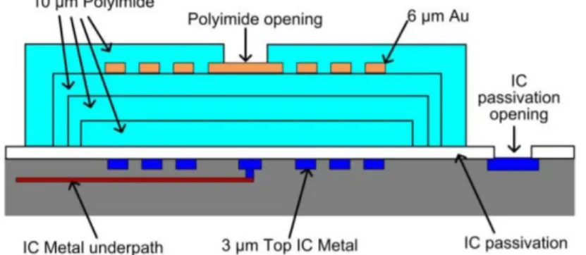
Micro-transformers using polyimide stacks have been used in other works, and an example of a transformer cross-section with a 30µm thick polyimide stack is shown in Figure 4 [2]. Aside from the dimensions, the cross-section of this architecture is expected to be similar. The thickness of the stack determined the 80µm radial spacing between the coils. This was done to equate the vertical breakdown path and the lateral breakdown path through the isolation barrier, in a similar manner to other works [3]. The shortest breakdown path would consequentially be 80µm of polyimide, which doubles the isolation provided by 40µm of polyimide.
Figure 4. Cross section of micro-transformer with 30µm polyimide spacing from A Fully Isolated Amplifier Based on
13
2.1.1.1 Coupling issue
The minimum spacing of 80µm between the inner and outer coils presents a problem for coupling windings in the lateral design. This can be understood by reviewing how the transformer operates.
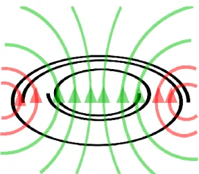
When an alternating current flows through the outer coil, a magnetic field will form around the windings of the coil. These magnetic field lines are illustrated as green and red vectors in Figure 5 below. The magnetic flux produced by this coil is the product of the vector of the magnetic field normal to the coil with the area of the coil. The
magnetic field will also flow through the inner coil, as it is concentric with the outer coil. The changing magnetic flux from the outer coil will consequentially result in an
electromotive force, or EMF, in the inner coil, which is how the transformer is able to transform voltages.
Figure 5. Representation of magnetic field lines resulting from current flow in coil.
14
However, because the area of the inner coil is significantly less than that of the outer coil due to the 80µm spacing that separates them, the changing flux of the inner coil will be significantly less. This is represented by green, coupled, magnetic field lines and red, uncoupled, magnetic field lines in Figure 5. The ratio of the magnetic flux shared by the two coils to the total flux generated is quantified as the coupling
coefficient between the two coils, often denoted by k. Less area shared by the two coils for the magnetic field to penetrate results in weaker coupling between them. Much research has gone into calculating the influence of coil placement with coupling, and the impact that poor coupling can have on the efficiency of the transformer [10]. The effect that poor coupling will have on this transformer’s performance will be seen by
15
2.1.1.2 Efficiency and Power delivery
The efficiency analysis of a single transformer has been researched extensively, and a summary of the analysis is explained below [11][12].
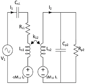
Figure 6. Coupled resonator model for a single transformer
Several component variables have been identified and labeled in the coupled resonator model shown in Figure 6. Impedances on the primary and secondary sides of the transformer have been condensed below to simplify later expressions.
𝑍1 = 𝑅𝑠1+ 𝑠𝐿𝑠1+ 1 𝑠𝐶𝑠1 𝑍2 = 𝑠𝐿𝑠2+ 1
1
16
The variable Rp2 represents the parallel combination of the load resistor with the series resistance of the secondary winding scaled by the square of its quality factor. This simplification was made using the narrow band approximation. The efficiency of the transformer is calculated in two steps. First, the efficiency between the primary winding and the secondary winding is found. This is done by finding the reflected impedance from the secondary across the primary winding.
𝑍𝑟𝑒𝑓12 =𝑉1 𝐼1 − 𝑍1
This is evaluated by performing Kirchhoff’s Voltage Law (KVL) along both isolated domains
𝑉1= 𝑍1𝐼1− 𝑠𝑀12𝐼2 𝑠𝑀12𝐼1 = 𝑍2𝐼2
By solving for the input current and output current, the impedance can be solved in terms of known variables. The reflected resistance is found by taking the real part of this value. 𝑍𝑟𝑒𝑓12 = − 𝑠 2𝑀 122 𝑠𝐿𝑠2+ 1 1 𝑅𝑝2+ 𝑠𝐶𝑝2
17 𝑅𝑟𝑒𝑓12 = 𝜔 2𝑘 122𝐿𝑠1𝐿𝑠2𝑅𝑝2 𝜔2𝐿 𝑠22+ (−1 + 𝜔2𝐶𝑝2𝐿𝑠2) 2 𝑅𝑝22
With the reflected resistance found, the efficiency between the primary and secondary windings can be found.
𝜂12 = 𝑅𝑟𝑒𝑓12 𝑅𝑠1+ 𝑅𝑟𝑒𝑓12 = 𝜔2𝑘122𝐿𝑠1𝐿𝑠2𝑅𝑝2 𝜔2𝑘 122𝐿𝑠1𝐿𝑠2𝑅𝑝2+ (𝜔2𝐿𝑠22+ (−1 + 𝜔2𝐶𝑝2𝐿𝑠2) 2 𝑅𝑝22) 𝑅𝑠1
The frequency that the circuit is oscillating at can be designed to maximize this efficiency. The ideal frequency can be found to be the resonant frequency of the secondary winding. It can be seen, therefore, that efficiency between the primary and secondary coils will be maximized when the primary and secondary windings are tuned to the same resonant frequency.
𝜔 → 1 √𝐿𝑠2𝐶𝑝2 𝜂12= 𝑘12 2 𝐿𝑠1𝑅𝑝2 𝑘122𝐿𝑠1𝑅𝑝2+ 𝐿𝑠2𝑅𝑠1
It is useful to see this efficiency in terms of the quality factors for each of the windings, as well as for the load.
18 𝑄𝑠1=𝐿𝑠1𝜔 𝑅𝑠1 𝑄𝑝2 = 𝑅𝑝2 𝐿𝑠2𝜔 𝑄𝐿 = 𝑅𝐿 𝐿𝑠2𝜔 𝜂12= 𝑘122𝑄𝑠1𝑄𝑝2 1 + 𝑘122𝑄𝑠1𝑄𝑝2
After the efficiency between the primary and secondary windings is found, the efficiency between the secondary winding and the load is calculated. As was described
previously, the resistor Rp2 is a parallel combination of the load resistance and the series resistance of the secondary scaled by Qs22. The efficiency, therefore, is found by treating the two resistors as a current divider.
𝜂2𝐿 = 1 𝑅𝐿 1 𝑄𝑠22𝑅𝑠2+ 1 𝑅𝐿 = 𝑄𝑠2 𝑄𝑠2+ 𝑄𝐿
The total efficiency of the transformer is found by taking the product of the two efficiencies found earlier: the efficiency from the primary to the secondary, and the efficiency of the secondary to the load.
𝜂1𝐿 = 𝜂12 𝜂2𝐿 = 𝑘12 2𝑄 𝑠1𝑄𝑠2𝑄𝑝2 (1 + 𝑘122𝑄𝑠1𝑄𝑝2)(𝑄𝑠2+ 𝑄𝐿) = 𝑘12 2 𝑄𝑠1𝑄𝑠22𝑄𝐿 (𝑄𝑠2+ 𝑄𝐿) (𝑄𝑠2+ 𝑄𝐿(1 + 𝑘122𝑄𝑠1𝑄𝑠2))
19
Because the efficiency is being defined as the ratio of the power delivered to the load to the total power generated from the source, the power delivery across the transformer falls out from this result.
𝑃𝐿 = 𝑉1,𝑟𝑚𝑠2 (𝑅𝑠1+ 𝑅𝑟𝑒𝑓14) 𝜂1𝐿 = 𝑘122𝑄𝑠1𝑄𝑠22𝑄𝐿𝑉12 2 (𝑄𝑠2+ 𝑄𝐿(1 + 𝑘122𝑄𝑠1𝑄𝑠2)) 2 𝑅𝑠1
As mentioned previously, the coupling coefficient between the two windings for a lateral design is expected to be poor due to the large spacing between them. Fortunately, this can be compensated by ensuring that the windings have large quality factors, which is to say low series resistance.
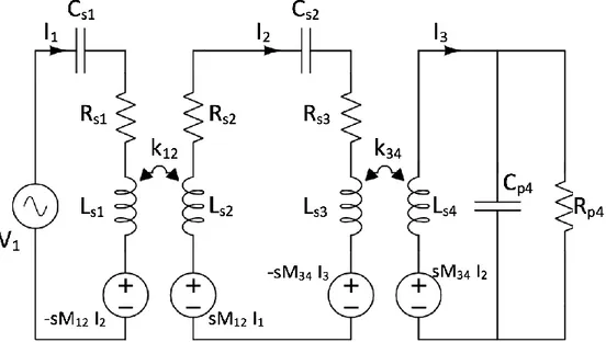
2.1.2 Back-to-Back
Similar to most integrated on-chip DC-DC converters, a back-to-back design utilizes stacked transformers. However, this architecture involves two transformers instead of one, where the secondary of the first transformer is connected to the primary of the second transformer.
20
Figure 7. Top-view of back-to-back design, half
Figure 8. Top-view of back-to-back design, full
Each planar spiral would be on its own gold layer, and the spirals would be vertically separated by a 40µm thick polyimide stack. The cross section of each transformer would be similar Figure 9. The two gold coils would be concentric and vertically separated by a 40µm layer of polyimide. By including a second transformer, there would be two polyimide isolation barriers between the input and output of the transformer die, consequentially doubling the isolation rating of a single polyimide stack. The result would be the desired 1500Vrms working voltage specification.
Figure 9. Cross section of a stacked with micro-transformer 32µm polyimide spacing from Integrated Signal and Power Isolation Provide Robust and Compact Measurement and
21
2.1.2.1 Efficiency and Power delivery
The steps for finding the efficiency of back-to-back transformers does not vary significantly from the single transformer case, and a summary of the analysis is below.
Figure 10. Coupled resonator model for back-to-back transformers
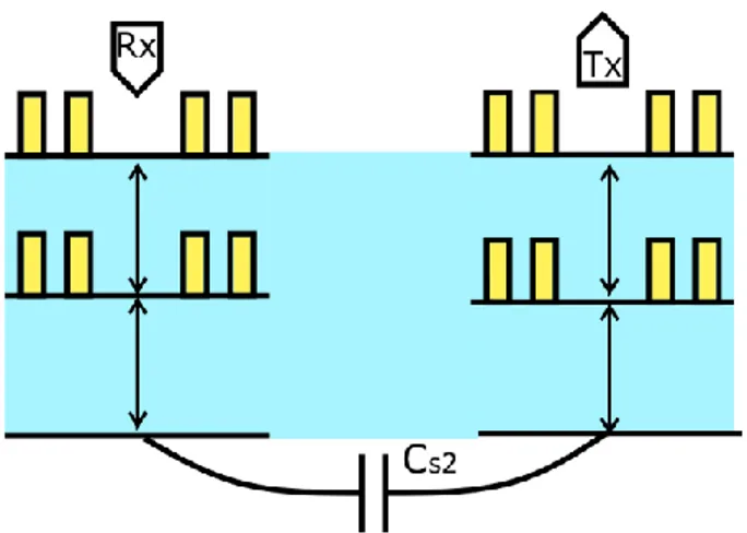
In the coupled resonator model shown in Figure 10, an extra capacitance has been introduced between the secondary of the first transformer and the primary of the second transformer. The purpose of this capacitor is to select the resonant frequency for the two windings it is interacting with. A possible way of implementing this is shown in Figure 11. The first transformer, connected to the oscillator, is denoted with an Rx, while the second transformer, connected to the rectifier, is denoted with a Tx. With the bottom coil of the first transformer as its secondary winding and the bottom coil of the second transformer as its primary winding, the capacitor can be added between them in the substrate.
22
Figure 11. Addition of tuning capacitor between two windings
Similar to the lateral case, impedances of the model are listed before. Similar to the single transformer case, the series resistance of the second transformer secondary – referred to as coil 4 for clarity – has also been scaled by its quality factor and
absorbed with the load resistance into the resistor Rp4.
𝑍1 = 𝑅𝑠1+ 𝑠𝐿𝑠1+ 1 𝑠𝐶𝑠1 𝑍2 = 𝑅𝑠2+ 𝑠𝐿𝑠2 𝑍3 = 𝑅𝑠3+ 𝑠𝐿𝑠3+ 1 𝑠𝐶𝑠2 𝑍4 = 𝑠𝐿𝑠4+ 1 1 𝑅𝑝4+ 𝑠𝐶𝑝4
23
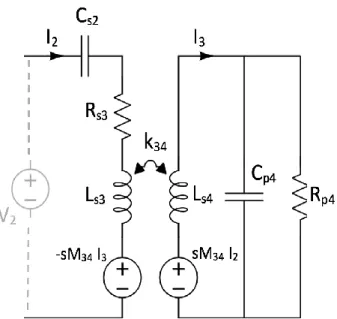
For simplicity, elements before coil 3 have been abstracted away into the source V2. This is to first find the reflected impedance from coil 4 to coil 3 – in other words, from the secondary to the primary of the second transformer.
Figure 12. Coupled resonator model focused around second transformer
The reflected impedance from coil 4 across coil 3 is found. This is then simplified by performing KVL around both isolated domains
𝑍𝑟𝑒𝑓34 =𝑉2 𝐼2 − 𝑍3
𝑉2 = 𝑍3𝐼2 − 𝑠𝑀34𝐼3 𝑠𝑀34𝐼2 = 𝑍4𝐼3
24 𝑍𝑟𝑒𝑓34 = − 𝑠2𝑀342 𝑍4 = − 𝜔 2𝑘 342𝐿𝑠3𝐿𝑠4 𝑖𝜔𝐿𝑠4+ 1 𝑖𝜔𝐶𝑝4+𝑅1 𝑝4
The real part of the impedance is used to find the reflected resistance
𝑅𝑟𝑒𝑓34 = 𝜔
2𝑘
342𝐿𝑠3𝐿𝑠4𝑅𝑝4 𝜔2𝐿
𝑠42+ (−1 + 𝜔2𝐶𝑝4𝐿𝑠4)2𝑅𝑝42
Because the efficiency will ultimately depend on this reflected resistance being as large as possible, the frequency can already be designed to maximize this value. By taking the derivative of the resistance and seeing which frequency sets it equal to zero, the designed frequency is found to be the resonant frequency of coil 4. The resulting reflected resistance and impedance are shown below.
𝜔 → 1 √𝐿𝑠4𝐶𝑝4 𝑍𝑟𝑒𝑓34 = −𝑖𝜔𝑘342𝐿𝑠3+𝑘34 2𝐿 𝑠3𝑅𝑝4 𝐿𝑠4 𝑅𝑟𝑒𝑓34 =𝑘34 2𝐿 𝑠3𝑅𝑝4 𝐿𝑠4
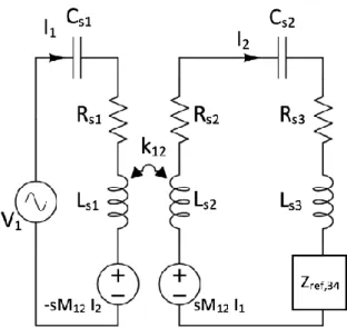
This reflected impedance will now be used to find the reflected impedance across both transformers. Figure 13 shows a simplified coupled resonator model that makes use of the reflected impedance.
25
Figure 13. Coupled resonator model focused around first transformer 𝑍𝑟𝑒𝑓14 =𝑉1 𝐼1 − 𝑍1 𝑉1 = 𝑍1𝐼1− 𝑠𝑀12𝐼2 𝑠𝑀12𝐼1 = (𝑍2+ 𝑍3+ 𝑍𝑟𝑒𝑓34)𝐼2 𝑍𝑟𝑒𝑓14 = − 𝑠 2𝑀 122 𝑍2+ 𝑍3+ 𝑍𝑟𝑒𝑓34 = − 𝜔 2𝑘 122𝐿𝑠1𝐿𝑠2 −𝜔𝐶𝑖 𝑠2+ 𝑖𝜔𝐿𝑠2+ 𝐿𝑠3(𝑖𝜔 + 𝑘34 2 (−𝑖𝜔 +𝑅𝐿𝑝4 𝑠4)) + 𝑅𝑠2+ 𝑅𝑠3
The real part of this value is the reflected resistance, and to maximize efficiency, this value should be as large as possible. The capacitance Cs2 can be designed to maximize the real part of this impedance.
26
𝐶𝑠2→ 1
𝜔2(𝐿
𝑠2+ (1 − 𝑘342)𝐿𝑠3)
It can be noted that this expression is equivalent to
𝜔 → 1
√(𝐿𝑠2+ (1 − 𝑘342)𝐿𝑠3)𝐶𝑠2
In other words, the frequency of oscillation needs to be the resonant frequency of a combination of coils 2 and 3. As seen before, these coils should also resonate with coil 4. The reflected resistance with these two conditions is the following
𝑅𝑟𝑒𝑓14 =
𝑘122𝐿𝑠1𝐿𝑠2
𝐶𝑝4(𝑘342𝐿𝑠3𝑅𝑝4+ 𝐿𝑠4(𝑅𝑠2+ 𝑅𝑠3))
The efficiency from coil 1, the first primary coil, to coil 4, the second secondary coil, can now be calculated. As before, it is useful to evaluate this in terms of quality factors
𝜂14 = 𝑅𝑟𝑒𝑓14 𝑅𝑠1+ 𝑅𝑟𝑒𝑓14 = 𝑘12 2 𝐿𝑠1𝐿𝑠2 𝑘122𝐿𝑠1𝐿𝑠2+ 𝐶𝑝4𝑅𝑠1(𝑘342𝐿𝑠3𝑅𝑝4 + 𝐿𝑠4(𝑅𝑠2+ 𝑅𝑠3)) 𝑄𝑠𝑥= 𝐿𝑠𝑥𝜔 𝑅𝑠𝑥
27 𝑄𝑝4 = 𝑅𝑝4 𝐿𝑠4𝜔 𝑄𝐿 = 𝑅𝐿 𝐿𝑠4𝜔 𝑄𝑝4 = 𝑄𝑠4𝑄𝐿 𝑄𝑠4+ 𝑄𝐿 𝜂14 = 𝑘12 2𝑄 𝑠1𝑄𝑠2𝑅𝑠2 (1 + 𝑘122𝑄𝑠1𝑄𝑠2)𝑅𝑠2+ (1 + 𝑘342𝑄𝑠3𝑄𝑝4)𝑅𝑠3
The efficiency between coil 4 and the load must then be found, identically to the single transformer case. 𝜂4𝐿 = 1 𝑅𝐿 1 𝑄𝑠42𝑅𝑠4 +𝑅1 𝐿 = 𝑄𝑠4 𝑄𝑠4+ 𝑄𝐿
The total efficiency of the architecture is taken as the product of these two values. The power delivery of this architecture falls out from this result.
𝜂1𝐿 = 𝑘122𝑄𝑠1𝑄𝑠2𝑄𝑠4𝑅𝑠2 (𝑄𝑠4+ 𝑄𝐿) ((1 + 𝑘122𝑄𝑠1𝑄𝑠2)𝑅𝑠2+ (1 + 𝑘342𝑄𝑠3𝑄𝑝4)𝑅𝑠3) 𝑃𝐿 = 𝑉1 2 2(𝑅𝑠1+ 𝑅𝑟𝑒𝑓14) 𝜂1𝐿 = 𝑘12 2𝑄 𝑠1𝑄𝑠2𝑄𝑠4𝑅𝑠2(𝑄𝑠4(𝑅𝑠2+ 𝑅𝑠3) + 𝑄𝐿(𝑅𝑠2+ (1 + 𝑘342𝑄𝑠3𝑄𝑠4)𝑅𝑠3)) 𝑉12 2𝑅𝑠1((1 + 𝑘122𝑄𝑠1𝑄𝑠2)(𝑄𝑠4+ 𝑄𝐿)𝑅𝑠2+ (𝑄𝑠4+ 𝑄𝐿(1 + 𝑘342𝑄𝑠3𝑄𝑠4)) 𝑅𝑠3) 2
28
2.1.3 Comparison
Designing a micro-transformer involves selecting the following dimensions, among others
• Outer radius • Number of turns • Turns ratio • Metal width
There are several characteristics that these dimensions effect, including the following
• Coupling coefficient • Inductance
• Series resistance • Quality factor
To understand the range of transformers that can result from either architecture discussed, multiple sweeps were performed on their dimensions. The extent of these sweeps is summarized below.
29
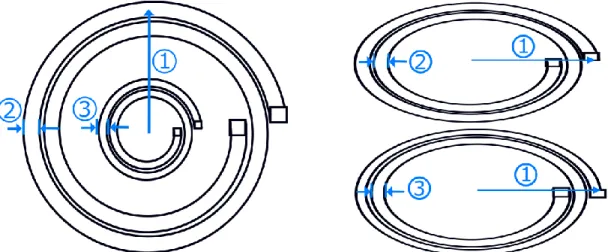
Figure 14. Simulated transformer layouts for sweeps; nested on the left and stacked on the right. Dimensions 1-3 represent outer radius, coil 1 metal width, and coil 2 metal
width, respectively
Characteristic Value
Outer radius 500um – 1mm
Number of turns, coil 1 1-30 Number of turns, coil 2 1-30
Metal width, coil 1 6um – 60um Metal width, coil 2 6um – 60um
Table 1. Sweep parameters
These sweeps were performed using ASITIC, a script-based simulator that can extract the characteristics of a transformer model given its geometry and process information. These sweeps were conducted at 200MHz, a frequency of the same magnitude as frequencies seen in several converters of this field that also allows for reasonably timed simulations. The results for a back-to-back transformer are expressed in Figures 15 – 17, while those for a lateral transformer are shown in Figures 18 – 20.
30
Figure 15. Quality factor against inductance for one stacked coil
Figure 16. Quality factor against inductance for other stacked coil
Figure 17. Quality factor against coupling coefficient for stacked transformer
31
Figure 18. Quality factor against inductance for nested coil
Figure 19. Quality factor against inductance for outer coil
Figure 20. Quality factor against coupling coefficient for nested transformer
32
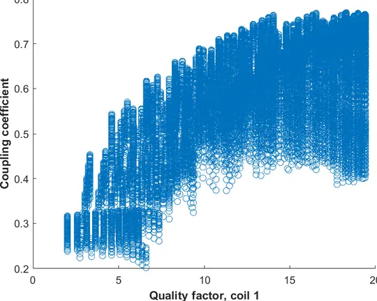
The coupling coefficient for a stacked transformer is reasonably large, reaching almost 0.8 in the limited sweeps conducted. A notable quality of the stacked
transformers is the disparity in the quality factors of its coils. While one coil of the transformer reaches a quality factor of nearly 20, the other coil does not exceed 9. This disparity is due to the positioning of the coils, as the proximity of the bottom coil to the substrate will increase the substrate losses in the coil and have adverse effects on its quality factor [14]. These results can be compared to a nested transformer, which would be used in the lateral case. As expected, the coupling coefficient for the lateral
architecture is significantly lower than that for the back-to-back case. However, the quality factors of both coils remain large, exceeding 20 each. Both coils are located on the same metal layer, and consequentially, they experience substrate losses equally.
Using these results, more specific representations for each architecture can be examined further. Values taken from the simulated sweeps can be used to calculate an expected efficiency and power delivery at 200MHz operation with a 5V input source. The transformer characteristics compared in Tables 2 and 3 were chosen such that the quality factors and coupling coefficients of the transformers were maximized for the sweep range tested. The back-to-back transformers used in this model are assumed to be symmetric, though asymmetrical cases are possible. Symmetry is chosen in this example, however, as this model represents the most promising transformer seen in simulation, so having a less promising transformer connected to it should not improve performance.
33
Table 2. Back-to-back transformer model characteristics, simulated at
200MHz
Table 3. Lateral transformer model characteristics, simulated at 200MHz
From Figures 21 and 22, it can be seen that the behavior of efficiency and output power as the load varies differ drastically. In the back-to-back case, an efficiency of 100% is theoretically achievable, but the efficiency falls off with the output load very quickly, and at a peak power delivery of 0.2W, the efficiency has fallen to approximately 50%. In the lateral case, the efficiency at which the peak output power is seen is also approximately 50%. However, the peak output power is 0.6W – three times higher than for the back-to-back model. Furthermore, when the output power is 0.4W, the efficiency is still roughly 73%. The lateral case demonstrates a more promising correlation
between power and efficiency, and consequentially, the lateral approach was chosen. Characteristic Value k 0.4 Qs1,2 25 Lp2 50nH Rs1 5Ω Characteristic Value k12, k34 0.8 Qs1,3 18 Lp2,s4 100nH Rs1,3 7Ω Qs2,4 8 Lp2,s4 50nH Rs2,4, 8Ω
34
Figure 21. Efficiency (left axis) and output power (right axis) against load resistance for back-to-back transformers from Table 1
Figure 22. Efficiency (left axis) and output power (right axis) against load resistance for lateral transformer from Table 2
35
Other factors that helped influence this decision were cost and footprint. One of the biggest deterrents for the lateral approach was the size of the transformer that would need to be chosen in order to offset the poor coupling between the two windings. However, the use of two stacked transformers is itself a large investment of space, and the configurations tested are approximately equal in footprint. Though maybe equally expensive in terms of footprint, the back-to-back design would undoubtedly be more costly because of the process it would require. A stacked transformer needs a process with two gold metal layers – one for each winding. Because a lateral design has both windings on the same layer, only one gold layer will need to be used. From a cost perspective, the lateral design is also more appealing.
36
Choosing a transformer for this project was an iterative process. The transformer influences the rectifier and oscillator designs by determining the operating frequency at which optimal performance is expected. At the same time, the oscillator and rectifier also influence what is needed from the transformer in terms of inductance and quality factor. Figure 23 shows only a sample of the lateral transformers that can be designed.
2.2 Rectifier
The transformer provides isolation, but also acts as an AC-AC converter – scaling an AC voltage from one terminal and outputting it to the other. For a full DC-DC converter, the AC output from the transformer will need to be rectified into a DC output. For this task, a rectifier must be designed. A full-wave rectifier makes use of both the positive and negative swing of the incoming AC signal, and in terms of efficiency, is the best option for this application. There are two full-bridge rectifiers that were strongly considered for this design: a center-tapped rectifier and a full H-bridge rectifier.
37
2.2.1 Center-tapped rectifier
Figure 24. Center-tapped rectifier circuit
A center-tapped rectifier allows for the secondary of the transformer to which it is receiving an AC signal to have its center-tap tied to the same ground that the output is referenced to. The chosen switch implementation for this rectifier chosen is shown in Figure 24. Active switches could have been used, but the diodes used are assumed to have sufficiently good efficiency without needing the overhead of gate drivers and added control circuitry, which could have their own losses. A closer look at that efficiency is detailed in [15] and summarized below.
38
Figure 25. Single state of center-tapped rectifier circuit with activated diode modeled as a voltage source with parasitic
resistance
The efficiency is being defined at the ratio of the power delivered to the output to the sum of the total power in the circuit. First, the power delivered to the load is calculated.
𝐼𝑜𝑢𝑡 = 1 𝜋∫ 𝐼1sin 𝜃 𝑑𝜃 𝜋 0 = 2 𝜋𝐼1 𝑃𝑜𝑢𝑡 = 𝐼𝑜𝑢𝑡2𝑅𝐿
The power dissipated in the diodes is then found
𝐼𝐷1,𝑟𝑚𝑠 = √ 1 2𝜋∫ (𝐼1sin 𝜃)2𝑑𝜃 𝜋 0 = 𝜋 4𝐼𝑜𝑢𝑡 𝐼𝐷1,𝑎𝑣𝑔= 1 2𝜋∫ 𝐼1sin 𝜃 𝑑𝜃 𝜋 0 = 1 2𝐼𝑜𝑢𝑡 𝑃𝐷 = 𝐼𝐷1,𝑟𝑚𝑠2𝑅𝐷+ 𝑉𝐷𝐼𝐷1,𝑎𝑣𝑔
39
Finally, the power dissipated in the capacitor is found. The capacitor is assumed to be non-ideal, and consequentially has a series resistance that will account for some loss.
𝐼𝐶,𝑟𝑚𝑠 = √1 2𝜋∫ (𝐼1sin 𝜃 − 𝐼𝑜𝑢𝑡)2𝑑𝜃 𝜋 0 = 𝐼𝑜𝑢𝑡√1 8(𝜋2 − 8) 𝑃𝐶 = 𝐼𝐶,𝑟𝑚𝑠2𝑅𝐶
The total efficiency is found to be the following
𝜂 = 𝑃𝑜𝑢𝑡
2𝑃𝐷+ 𝑃𝐶 + 𝑃𝑜𝑢𝑡 =
8𝐼𝑜𝑢𝑡𝑅𝐿 𝐼𝑜𝑢𝑡𝜋2𝑅
𝐷 + 8𝐼𝑜𝑢𝑡𝑅𝐿+ 8𝑉𝐷+ (𝜋2− 8)𝐼𝑜𝑢𝑡𝑅𝐶
An important metric for designing this rectifier is the switch stress parameter for the diodes. This is the product of the peak current stress and the peak voltage stress that each of the diodes will experience. This will influence the sizing of the diodes and how many would have to be used in series.
𝐼𝐷1,𝑚𝑎𝑥= 𝐼1 = 𝜋 2𝐼𝑜𝑢𝑡 𝑉𝐷1,𝑚𝑎𝑥 = 2𝑉𝑜𝑢𝑡 = 2𝑃𝑜𝑢𝑡
𝐼𝑜𝑢𝑡 𝑆𝑆𝑃 = 𝜋𝑃𝑜𝑢𝑡
40
The output power capability is defined as the ratio of the power output to the switch stress parameter and provides insight on the output power possible at a given maximum current and voltage through the diode.
𝑐𝑝𝑟 =𝑃𝑜𝑢𝑡 𝑆𝑆𝑃 =
1 𝜋
2.2.2 H-bridge rectifier
Figure 26. H-bridge rectifier circuit
The passive H-bridge rectifier is another full-wave rectifier that is very common for on-chip isolated dc-dc converters. Similar to the center-tapped rectifier, passive switches – diodes – were used instead of active switches because the diodes available are assumed to be efficient enough to avoid the added complexity of control.
41
Figure 27. Single state of H-bridge rectifier circuit with activated diode modeled as a voltage source with parasitic resistance
The efficiency is shown below. This function is very similar to the center-tapped case, with the only variation being in the diode loss. However, the diodes to be used are already assumed to be relatively efficient, so any advantage of the center-tapped
solution in this respect is negligible.
𝜂 = 𝑃𝑜𝑢𝑡
4𝑃𝐷+ 𝑃𝐶 + 𝑃𝑜𝑢𝑡 =
8𝐼𝑜𝑢𝑡𝑅𝐿 2𝐼𝑜𝑢𝑡𝜋2𝑅
𝐷 + 8𝐼𝑜𝑢𝑡𝑅𝐿 + 16𝑉𝐷+ (𝜋2 − 8)𝐼𝑜𝑢𝑡𝑅𝐶
The switch stress parameter for the diodes in the H-bridge rectifier is shown below.
𝐼𝐷1,𝑚𝑎𝑥= 𝐼1 = 𝜋 2𝐼𝑜𝑢𝑡 𝑉𝐷1,𝑚𝑎𝑥 = 𝑉𝑜𝑢𝑡 = 𝑃𝑜𝑢𝑡 𝐼𝑜𝑢𝑡 𝑆𝑆𝑃 =𝜋 2𝑃𝑜𝑢𝑡
42 𝑐𝑝𝑟 =𝑃𝑜𝑢𝑡
𝑆𝑆𝑃 = 2 𝜋
The H-bridge has a switch stress parameter that is one half the switch stress parameter for the center-tapped case. This means that diodes experiencing the same maximum currents and voltages as the center-tapped case will result in twice the output power. With comparable efficiency and twice the output power capability, the H-bridge rectifier was selected.
2.3 Oscillator
With the transformer and rectifier selected, the system is currently capable of AC-AC conversion followed by AC-AC-DC conversion. The final piece needed for the full DC-DC converter is circuitry capable of DC-DC-AC conversion, as the input to the system is expected to be a DC source while an AC signal is needed for mutual inductance to occur in the transformer windings. This is known as an oscillator and it will be
responsible for driving the isolator. The oscillator used in this work draws inspiration from two oscillator topologies: A cross-coupled LC tank oscillator and a Class E oscillator
43
2.3.1 Cross-coupled LC Tank
Figure 28. Cross-coupled LC Tank oscillator
The cross-coupled LC Tank oscillator architecture shown above is very common for integrated DC-DC power supplies, and its operation has been extensively analyzed [16]. This negative impedance oscillator can be broken up into two parts: a cross-coupled pair and an LC tank. The impedance seen by the LC-tank looking into the cross-coupled pair is negative, with a magnitude of half of the transconductance of one of the active switches. When this negative impedance matches the magnitude of
damping resistances in the circuit, stable oscillation at the resonant frequency of the LC tank occurs. While a viable candidate for an oscillator, research has already been
conducted to improve the cross-coupled LC tank. This design, therefore, is considered a starting point.
44
2.3.2 Single-ended Class E
Figure 29. Single-ended class E power amplifier
In order to try to improve the efficiency of the oscillator, inspiration was drawn from the class E power amplifier. This amplifier has two states: the state where the active switch is on, and the state where the switch is off. In the state where the switch is on, current is flowing through the switch, and the voltage across the switch and
capacitor is zero. The matching network formed by L and Ca allow sinusoidal current to flow to the load R at a specific frequency. The inductor between the source and the active switch is assumed to be large, and its current can be approximated to be DC. The current that would be flowing through the switch is therefore the difference of the DC current funneled from the source and the AC current being delivered to the load. In the state where the switch is off, current flow through the switch is now zero. However, the DC feed inductor continues to funnel the same amount of DC current to the circuit,
45
and because the current provided to the load through the matching network is also unchanged, the current originally flowing through the switch now must flow through the capacitor Cs. This produces a voltage across the capacitor and the switch. If a voltage is still present across the capacitor when the switch it returns to the on state, the capacitor will immediately discharge through the switch and any non-ideal series resistances it has. This form of power dissipation is known as switching loss, and can be reduced by soft-switching, which is to say reducing the voltage across the switch as low as possible before turning it back on. When the voltage across the switch is zero before it is turned on, zero-voltage switching is achieved, and switching losses in the circuit are effectively eliminated. Based on the capacitor relationship 𝐼 = 𝐶𝑑𝑉
𝑑𝑡, the derivative of the switch voltage at any point during this state can be found. The component values in a class E amplifier can be selected in such a way that the derivative of the switch voltage at the time the switch will be turned on can be set to zero, resulting in zero-voltage switching and, theoretically, 100% efficiency.
For the purpose of the DC-DC converter being designed, a differential implementation of this oscillator is preferred to a single ended approach. While this could be implemented with two single ended amplifiers with inverted inputs, a self-driven oscillator would also be desirable, as was the case for the cross-coupled LC tank. Converting class E amplifiers into self-driven power oscillators for improved efficiency has been previously researched and show promising results [7][17].
46
2.3.3 Cross-coupled Class E
Figure 30. Proposed cross-coupled class E oscillator
The proposed architecture for this work is shown in Figure 30 and will be referred to as a cross-coupled class E oscillator. Comparable to the cross-coupled LC tank oscillator, this is a self-driven oscillator that does not require extra control circuitry to drive the gates of the active switches. The LC-tank is no longer determined by the isolating transformers, but instead by two smaller inductors, which would constitute DC feed inductors in a single ended class E amplifier. This allows the isolating transformer’s primary to be implemented at the load of the cross-coupled pair, where the center-tap is now able to be tied to ground. This helps the EMI of the circuit by reducing the path of common mode currents. The transformer primary forms a matching network with the Ca capacitors, which AC couple the oscillator to the transformer.
47
2.3.3.1 DC Feed inductor
The single-ended Class E converter is typically implemented with an RF choke – an inductor large enough to filter any AC components and deliver only DC current from the source. An integrated choke, however, is not very feasible as a planar transformer in this application. To have a large enough inductance to constitute a choke, many
windings will be needed, each spiraling out from the inner most winding. This will result in a winding with an excessively large foot print, and presumably poor quality factor. The average voltage drop across the inductor in periodic steady state is ideally zero, but a voltage drop will be present across any series resistance it has, the magnitude of which is inversely proportional to the quality factor. This voltage drop not only presents a continuous loss to the system, but also reduces the average voltage across the active switch, which determines the amplitude of the AC signal seen by the transformer. An inductor with poor quality factor, therefore, will quickly degrade the performance of the oscillator.
Research has shown that an RF choke is not needed in a single-ended class E oscillator, and that a smaller inductor in its place, when chosen properly can even improve the efficiency of the oscillator [18]. The equations found in research are difficult to implement in a self-oscillating case, but empirically, an acceptably small inductor value can be found.
48
The implementation of the two inductors as a single transformer was
investigated. Because the size of the inductor needed to gain sufficient inductance is a concern, a lateral transformer similar to the isolator is not a feasible option, as it
requires a large outer radius for the coils to be nested. A stacked transformer would be more feasible. The two inductors in this oscillator expected to be equivalent, however, and the bottom coil is expected to have a lower quality factor due to substrate losses, as was discussed previously.
2.3.3.2 Level shifting
The voltage across the drain of the cross coupled devices can get relatively large. Assuming the quality factor of the inductors is large enough, the average voltage across the drain of the device is expected to be approximately VDD. The peak voltage, therefore, will be πVDD. This is too large for NMOS devices, so LDMOS devices will be used, as they are better suited for high power applications. Because the cross-coupled devices have their drains and gates tied to one another, those terminals are expecting to see the same voltage. LDMOS devices have lower gate voltage ratings than drain voltage ratings. This means that the drain voltage for an LDMOS will need to be level shifted before safely being applied to the gate. This is done with a capacitor divider. By implementing a single capacitor between the drain and gate, this will form a divider with the capacitance of the LDMOS between the gate and source. This capacitive voltage divider will then determine the ratio of the peak voltage across the drain to the peak voltage across the gate.
49
Figure 31. Capacitive voltage divider to level-shift gate of active switch
3. Simulation
Figure 32. Proposed DC-DC converter circuit
The DC-DC converter was designed for a 5V-5V conversion, and the full topology of the circuit simulated can be seen in Figure 32. This design was heavily iterated, and the component values listed below empirically showed the best results.
50
Ca 300pF CL 450pF
Cs 1pF RL 50Ω
Cshift 46pF Ct 12pF
Table 4. DC-DC converter component values
The dimensions of the transformer used in simulation are displayed and
quantified in Figure 33 and Table 5, and its resulting characteristics are shown in Table 6. The transformer used was chosen for the large quality factors of each of its windings, and its high predicted efficiency even at high frequencies.
Figure 33. Transformer layout. Dimensions 1-3 correspond to isolation spacing, gold trace width, and outer radius values found on Table 3, respectively. The transformer
windings are terminated with bond pads.
Gold trace width 100µm
Outer radius 1mm
Isolation spacing 80µm
Turns spacing 6µm
Turns ratio 2:2
51 Primary Secondary Q 27.75 Q 27.19 L 4.74nH L 6.14nH R 0.64Ω R 0.86Ω Both k 0.37
Table 6. Transformer characteristics, simulated at 600MHz
Figure 34. Quality factor of inner coil against frequency
Figure 35. Quality factor of outer coil against frequency
Figure 36. Simulated efficiency of chosen transformer against frequency
52
Width 4µm Length 4µm In parallel 200
Table 7. Diode specifications. Each diode symbol in Figure 32 represents 200 diodes in parallel
Length/device 50µm Width 0.6µm Number of gates 280
Max Vgs 5.5V Max Vds 18V
Table 8. LDMOS transistor specifications
Metal trance width 26µm
Turns 8
Area 0.117 mm2
Inductance 19nH
Quality Factor 8
Table 9. DC feed inductor specifications
The performance of the converter in its entirety while operating in steady state is summarized in Table 10 and the waveforms that follow. The goal of this project was to increase the working voltage while being able to delivery at least 500mW output power with at least 30% efficiency. Based on simulation, this topology is expected to deliver over 1W of output power at 50% efficiency. Though the scope of this work is limited to the simulation phase, and performance will invariably worsen after implementation, these are promising results for DC-DC converters with improved isolation.
53 Total efficiency 50% Driver efficiency 74% Transformer efficiency 77% Rectifier efficiency 86% Output power 1.1W Operating frequency 480MHz
Table 10. DC-DC converter performance
Figure 37. Gate voltage of an LDMOS transistor in cross-coupled pair
Figure 38. Drain voltage of an LDMOS transistor in cross-coupled pair
Figure 39. Voltage across secondary windings of the isolating transformer and the rectified output voltage of the converter
54
4. Future Work
From simulations run on the DC-DC converter design this work proposes, efficiency and power delivery projections far exceed the minimum specifications set for this project. The proposed design utilizes a transformer with a 1mm outer radius, a size that contributes to a relatively high quality factor to offset poor coupling. However, this transformer is much larger than those seen in related works and would be far too
expensive to realistically implement. Unsurprisingly, reducing the size of the transformer is seen as a priority. The amount by which it can be minimized, however, needs further analysis, as the performance of the converter might also be effected by the needed additions of load regulation and bond wires.
4.1 Load Regulation
When this DC-DC converter is implemented, one concern is how to implement load regulation. In order for the output voltage to avoid overshoot from the desire value, feedback will be added Though the control of this feedback has not been looked at extensively for this work, a proof of concept is below.
55
Figure 40. Proposed oscillator with load regulation transistors
This feedback will require the addition of two more active switches, shown in Figure 40. Each has their drain tied to one of the gates of the cross-coupled pair, and their source tied to ground. Because the drain voltage of the transistors is limited to the gate voltage of the cross-coupled pair, using NFETs for the feedback transistors is acceptable. If the output voltage overshoots, a positive gate voltage will be applied to the gates of the feedback transistors. This will cause both transistors to enter saturation, which will effectively tie the gates of the cross-coupled pair to ground. With their gates tied to ground, current flowing into the transformer will be cut-off, decreasing the output voltage. As the output voltage falls to an acceptable voltage, the gates of the feedback transistors will be set to ground, and the cross-coupled pair will be free to oscillate once again. More work must be done to implement this and examine the cost of this addition.
56
Figure 41. Example of a turn off event with load regulation transistors
4.2 Bond wires
Bond wire will be used to connect the transformer die to the driver die and
rectifier die, but they will introduce extra capacitance, inductance, and series resistance that will affect the efficiency and operating frequency of the system. An approximate circuit model referenced for the bond wire is shown in Figure 42 [19].
57
Lbw 1nH Rbw 40mΩ Cbw 70pF
Table 11. Parameters for 1mm gold bond wire model with 1.2 mil diameter
The inductance of this model is on the order of nanohenries, which is also the same order of magnitude as the inductance of the transformer. Because of this, there is a concern that the addition of the bond wire will affect the operating point of the
converter. There are methods to minimize the effect of these parasitics and including multiple bond wires in parallel to minimize their overall impedance is a possibility. However, the extent at which the bond wires will interfere with performance should be fully scoped.
58
Bibliography
[1] B. Chen, "Fully Integrated Isolated DC-DC Converter Using Micro-Transformers." Twenty-Third Annual IEEE Applied Power Electronics Conference and Exposition, pp. 335-338, Feb. 2008.
[2] S. Ma et al., “A Fully Isolated Amplifier Based on Charge-Balanced SAR Converters.” IEEE Transactions on Circuits and Systems I: Regular Papers, vol. 65, no. 6, pp. 1795-1804, Jun. 2018.
[3] Y. Moghe, A. Terry, and D Luzon, “Monolithic 2.5kV RMS, 1.8V - 3.3V Dual-Channel 640Mbps Digital Isolator in 0.5µm SOS.” 2012 IEEE International SOI Conference, Napa, CA, Oct. 2012.
[4] R. Yun, J. Sun, E. Gaalaas, and B. Chen, “A Transformer-based Digital Isolator With 20kVPK Surge Capability and > 200kV/µS Common Mode Transient Immunity.” 2016 IEEE Symposium on VLSI Circuits, Honolulu, HI, pp. 1-2, Sept. 2016.
[5] N. Spina et al., “Current-Reuse Transformer-Coupled Oscillators with Output Power Combining for Galvanically Isolated Power Transfer Systems.” IEEE Transactions on Circuits and Systems I: Regular Papers, vol. 62, no. 12, pp. 2940-2948, Dec. 2015.
[6] N. Greco, A. Parisi, G. Palmisano, N. Spina, and E. Ragonese, “Integrated transformer modelling for galvanically isolated power transfer systems,” in Proc. 13th Conf. Ph.D. Res. Microelectron. Electron. (PRIME), Jul. 2017, pp. 325–328.
[7] Q. Ma et al., “Power-Oscillator Based High Efficiency Inductive Power-Link for Transcutaneous Power Transmission.” Fifty-Third IEEE International Midwest Symposium on Circuits and Systems, pp. 537-540, Aug. 2010.
[8] N. Greco et al., “A 100-mW Fully Integrated DC-DC Converter with Double Galvanic Isolation.” Forty-Third IEEE European Solid State Circuits Conference, pp. 291-294, Nov. 2017.
[9] V. Fiore, E. Ragonese, G. Palmisano, "A Fully Integrated Watt-Level Power Transfer System with On-Chip Galvanic Isolation in Silicon Technology." IEEE Transcripts Transactions on Power Electronics, vol. 32, no. 3, pp. 1984-1995, Mar. 2017.
[10] R.M. Duarte, G.K. Felic, “Analysis of the Coupling Coefficient in Inductive Energy Transfer Systems.” Active and Passive Electronic Components, vol. 2014, pp. 1-6, Jun. 2014.
59
[11] M. Gasulla et al., “Correction to ‘Feedback Analysis and Design of RF Power Links for Low-Power Bionic Systems’.” IEEE Transactions on Biomedical Circuits and Systems, vol. 8, no. 1, pp. 148-149, Feb. 2014.
[12] M. Baker and R. Sarpeshkar, “Feedback Analysis and Design of RF Power Links for Low-Power Bionic Systems.” IEEE Transactions on Biomedical Circuits and Systems, vol. 1, no. 1, pp. 28-38, Jul. 2007.
[13] B. Chen, “Integrated signal and power isolation provide robust and compact
measurement and control,” Analog Devices, Norwood, MA , Tech. Rep. 2013. [Online]. Available:
http://www.analog.com/media/en/technical-documentation/technical- articles/Integrated-Signal-and-Power-Isolation-Provide-Robust-and-Compact-Measurement-and-Conrol-MS-2511.pdf
[14] M.Z. Yang, C.L. Dai, and J.Y. Hong, “Manufacture and characterization of high Q-factor inductors based on CMOS-MEMS techniques” Sensors (Basel, Switzerland) vol. 11, Oct. 2011.
[15] M.K. Kazimierczuk, “Class D Current-Driven Rectifiers for Resonant DC /DC Converter Applications”, IEEE Transactions on Industrial Electronics, vol. 38, pp. 344-354, Nov. 1991.
[16] J.S. Hamel, “LC Tank Voltage Controlled Oscillator Tutorial “, Presented to the UW ASIC Analog Group. [Online]. Available: http://www.asic.uwaterloo.ca/filesvcotut.pdf.
[17] R. Pinto, R. Duarte, F. Sousa, I. Muller, and V. Brusamarello, “Efficiency modeling of class-E power oscillators for wireless energy transfer.” 2013 IEEE Instrumentation and Measurement Technology Conference, pp. 271–275, May 2013.
[18] D. Milosevic, J. van der Tang, and A. van Roermund, “Explicit design equations for class-E power amplifiers with small dc-feed inductance,” Proceedings of the 2005 European Conference on Circuit Theory and Design, vol. 3, pp. 101–104, Aug. 2005.
[19] N. Karim, “Plastic Packages’ Electrical Performance: Reduced Bond Wire Diameter.” AMKOR Electronics, Inc., Chandler, AZ, USA, 2002. [Online]. Available: