Publisher’s version / Version de l'éditeur:
ACS Nano, 2017-11-01
READ THESE TERMS AND CONDITIONS CAREFULLY BEFORE USING THIS WEBSITE. https://nrc-publications.canada.ca/eng/copyright
Vous avez des questions? Nous pouvons vous aider. Pour communiquer directement avec un auteur, consultez la
première page de la revue dans laquelle son article a été publié afin de trouver ses coordonnées. Si vous n’arrivez pas à les repérer, communiquez avec nous à [email protected].
Questions? Contact the NRC Publications Archive team at
[email protected]. If you wish to email the authors directly, please see the first page of the publication for their contact information.
NRC Publications Archive
Archives des publications du CNRC
This publication could be one of several versions: author’s original, accepted manuscript or the publisher’s version. / La version de cette publication peut être l’une des suivantes : la version prépublication de l’auteur, la version acceptée du manuscrit ou la version de l’éditeur.
For the publisher’s version, please access the DOI link below./ Pour consulter la version de l’éditeur, utilisez le lien DOI ci-dessous.
https://doi.org/10.1021/acsnano.7b07068
Access and use of this website and the material on it are subject to the Terms and Conditions set forth at
Resolving and tuning carrier capture rates at a single silicon atom gap
state
Rashidi, Mohammad; Lloyd, Erika; Huff, Taleana R.; Achal, Roshan; Taucer,
Marco; Croshaw, Jeremiah J.; Wolkow, Robert A.
https://publications-cnrc.canada.ca/fra/droits
L’accès à ce site Web et l’utilisation de son contenu sont assujettis aux conditions présentées dans le site LISEZ CES CONDITIONS ATTENTIVEMENT AVANT D’UTILISER CE SITE WEB.
NRC Publications Record / Notice d'Archives des publications de CNRC:
https://nrc-publications.canada.ca/eng/view/object/?id=b681fbd1-f23a-452f-b3de-d297f86471a9 https://publications-cnrc.canada.ca/fra/voir/objet/?id=b681fbd1-f23a-452f-b3de-d297f86471a9
Resolving and Tuning Carrier Capture Rates at
a Single Silicon Atom Gap State
Mohammad Rashidi,
*
,†,‡,∥Erika Lloyd,
†,∥Taleana R. Huff,
†,§Roshan Achal,
†,§Marco Taucer,
†Jeremiah J. Croshaw,
†and Robert A. Wolkow
†,‡,§†
Department of Physics, University of Alberta, Edmonton, Alberta T6G 2J1, Canada
‡
National Institute for Nanotechnology, National Research Council of Canada, Edmonton, Alberta T6G 2M9, Canada
§
Quantum Silicon, Inc., Edmonton, Alberta T6G 2M9, Canada
ABSTRACT: We report on tuning the carrier capture events at a single dangling bond (DB) midgap state by varying the substrate temperature, doping type, and doping concentration. All-electronic time-resolved scanning tunnel-ing microscopy (TR-STM) is employed to directly measure the carrier capture rates on the nanosecond time scale. A characteristic negative differential resistance (NDR) feature is evident in the scanning tunneling microscopy (STM) and scanning tunneling spectroscopy (STS) measurements of DBs on both n- and p-type doped samples. We find that a common model accounts for both observations.
Atom-specific Kelvin probe force microscopy (KPFM) measurements confirm the energetic position of the DB’s charge transition levels, corroborating STS studies. We show that under different tip-induced fields the DB can be supplied with electrons from two distinct reservoirs: the bulk conduction band and/or the valence band. We measure the filling and emptying rates of the DBs in the energy regime where electrons are supplied by the bulk valence band. We show that adding point charges in the vicinity of a DB shifts observed STS and NDR features due to Coulombic interactions.
KEYWORDS: silicon, dangling bonds, time-resolved scanning tunneling microscopy, noncontact atomic force microscopy, carrier-capture rates
W
hether for the next era of computing or an improvement of current technology, detailed studies of individual atoms in semiconductors are re-quired.1,2 One important issue is the dynamics of deep levels in the semiconductor band gap.3,4In some exotic applications, these deep gap states can act as the device itself.STM and charge-sensitive noncontact atomic force micros-copy (NC-AFM) are ideal tools to investigate deep gap states on the atomic scale. Owing to the recent development of TR-STM techniques, today it is possible to study the dynamic processes of single atoms and molecules with time resolution down to a fraction of a picosecond.5−12 Examples are the measurement of the spin relaxation of individual atoms,6 imaging the ultrafast carrier capture into a single quantum dot,13nanosecond resolved study of single arsenic dopants14,15 and femtosecond orbital imaging of a single molecule.16
One particular technologically relevant gap state is the surface state of a silicon DB. DBs are promising candidates to be employed as building blocks in field controlled computing designs17 and as charge qubits.18−20 They can be place-d21−23and erased24,25 with atomic precision. Confined quantum-well states can be fabricated by linking DBs in a linear chain.26Prior STM and STS analyses have provided both
a detailed description of carrier capture by DBs into their gap state27and examination of the Coulomb repulsion energy for a single silicon DB.28 Recently, it has been shown that the Coulomb energy separating the two different charge states of a DB, the Hubbard “U”, gives rise to a characteristic NDR feature.29In the same study, the carrier capture rate into that midgap state was directly measured by employing all-electronic TR-STM.
Here, we explore previously inaccessible carrier capture events at a single DB gap-state on hydrogen-terminated Si(100) (H−Si) to thereby expand upon measurement and control of silicon bulk to surface-state transport. Studies of n- and p-type samples reveal that both doping types exhibit a characteristic NDR feature. We employ TR-STM to directly measure the majority carrier transition rate from the bulk to the DB on the nanosecond time scale. We alter the majority carrier concentration at the surface by annealing the substrate at different temperatures and show its effect on the capture rate. We show that the tip-induced band bending can draw the DB’s Received: October 5, 2017
Accepted: November 1, 2017 Published: November 1, 2017
Article
www.acsnano.org
© XXXX American Chemical Society A DOI:10.1021/acsnano.7b07068
ACS NanoXXXX, XXX, XXX−XXX Cite This: ACS Nano XXXX, XXX, XXX-XXX
energetic position down to make it resonant with the bulk valence band. In this configuration, the DB can be supplied by the valence band in addition to the conduction band. The filling and emptying rates of the DB in this energy regime are also measured using a variant of all-electronic pump probe methods. In addition, we use atom-specific KPFM measurements to probe the bias voltages where DB charge-state transitions occur. Furthermore, single-point charges were added in the vicinity of a DB to modify both the DB’s supply rate from the bulk as well as the relative energetic position of the charge transition levels of that DB.
RESULTS AND DISCUSSION
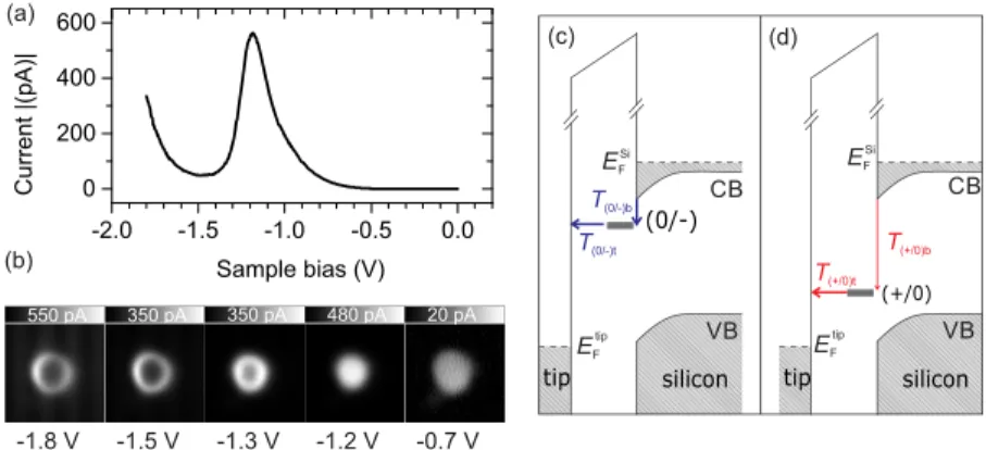
The NDR phenomenon was first observed by Esaki in tunnel diodes.30It has been observed that DBs on degenerately doped silicon surfaces also exhibit NDR.27−29 Figure 1a displays the
I(V) spectroscopy of a DB on a degenerately n-doped
hydrogen-terminated Si(100). The tunneling current first rises with increasing negative sample bias voltage but decreases again (NDR) at approximately −1.20 V. As shown inFigure 1b, in the NDR energy regime, the DB’s center is less conductive than its edge, resulting in a “ring” shape. A detailed description of the NDR feature and its properties can be found in a previous work.29 Briefly, when the DB transitions from a predominantly neutral state to a positive condition, a nonresonant inelastic process becomes dominant. This results in a reduced carrier capture rate at the DB.
Parts c and d ofFigure 1display the energy band diagrams of our system in the NDR energy regime. H−Si(100) has no localized surface states. When the surface is degenerately doped on n-type samples, the Fermi level is above the conduction band (impurity band). For this doping condition, DBs are natively negatively charged; i.e., they hold two electrons. Different STM measurement conditions can change the occupation of the DB to hold either one electron (neutral charge state) or zero electrons (positive charge state).14,31,32 The charge transition levels are represented by (+/0) and (0/ −) in Figure 1c,d. These levels denote the energy required to add the first and second electron to the DB, respectively.
The energy difference between the charge transition levels arises from the Coulomb repulsion between the two electrons occupying the same DB orbital. As a result, the two transition levels are mutually exclusive: the DB cannot be singly and
doubly occupied at the same time, and the (0/−) transition level is irrelevant unless the DB is already occupied by at least one electron. The (0/−) level acts as a stepping stone via vibronic coupling33for the conduction band electrons to reach the tip, but only as long as the DB holds at least one electron (Figure 1c). The DB can occasionally be fully emptied by the tip, making it positively charged (Figure 1d). When the DB is positively charged, the (0/−) level is not available for the electron to tunnel efficiently to the tip. The conduction of electrons from the bulk to the tip through the DB stops during this time until one electron transitions from the conduction band to the (+/0) level, making the DB neutral again. Since this process is inelastic, this transition is slow. Direct measurements show that the rate electrons pass from the conduction band to the (+/0) level is at least 2 orders of magnitude slower than the rate to reach the (0/−) level from the conduction band.29This slow inelastic process is the origin of NDR.
Figure 2a compares I(V) spectroscopy measurements of a DB and H−Si site at decreasing tip−sample distances. Importantly, the DB is conductive in the band gap of silicon. At these energies, the current is through the (0/−) level of the DB, meaning it is always at least singly occupied. Comparing to the spectra acquired over H−Si, we see that there is nearly no measurable current in the gap, except at the closest tip−sample separations, where the overlap between the tip and sample wave functions becomes sufficient to see the current originating from the donor band. These measurements again corroborate that the direct tunneling from the conduction band to the tip is very weak compared to having the DB gap state as a stepping stone. Figure 2b shows similar curves toFigure 2a but extended to show the spectroscopy up to a sample bias of −2.0 V. For the tip-height offset of 0 pm, the NDR feature is absent in the I(V) spectroscopy of the DB due to the slow emptying rate from the (+/0) level to the tip.29As the tip moves closer to the surface (starting with the −100 pm tip height offset), the NDR feature appears at approximately −1.20 V. By increasing the emptying rate with closer tip−sample distances (closer than −300 pm tip-height offset), we are able to make the DB spend a significant fraction of its time in the positive charge state. The positively charged DB becomes clear when the conduction over the DB becomes smaller than H−Si at the same tip height. The point where this occurs is indicated by the arrows inFigure 2b. The positively charged DB is less conductive than H−Si because the Figure 1. (a) I(V) spectroscopy of a single DB on a degenerately doped n-type H−Si(100) surface showing the characteristic NDR feature at approximately −1.20 V. (b) Constant height STM images of the DB at different bias voltages displaying its characteristic “ring” shape in the NDR energy regime. (c, d) Energy diagrams of the two conduction pathways in the NDR energy regime. (+/0) and (0/−) denote the charge transition levels of the DB. CB and VB indicate the sample’s conduction and valence bands. The Fermi level of the tip and the sample are denoted by EFtipand EFSi. T(0/−)b, T(+/0)b, T(0/−)t, and T(+/0)tdenote the time constant of electron transition from the bulk to the (0/−) level,
from the bulk to the (+/0) level, from the (0/−) level to the tip and from the (+/0) level to the tip, respectively.
ACS Nano Article
DOI:10.1021/acsnano.7b07068
ACS NanoXXXX, XXX, XXX−XXX
electron conduction from the bulk impurity band to the tip via the DB’s (+/0) level is inelastic and therefore slow. At the same time, the charge-induced downward band bending of the valence band in the presence of a positively charged DB reduces the direct tunneling from the valence band to the tip. The KPFM measurement in Figure 3a shows the bias voltages where the charge transitions on an n-type sample occur. The steplike jump in the frequency shift vs bias voltage
signal at approximately −0.20 V corresponds to a single-electron charge transition, consistent with previous studies that report steplike features in KPFM experiments for single-charge-state switching events.34,35The DB goes from a negative charge state right of the step to a neutral charge state on the left.18We also observe a secondary feature just before the onset of the NDR regime, a small dip in the frequency response at approximately −1.10 V. This dip is associated with an average charge population change of DB from neutral (right of the dip) to positive (left of the dip) similar to the prior works where continuous changes in the charge state led to diplike features in KPFM measurements.36−39 A more comprehensive and quantitative understanding of the secondary feature in relation to its time-averaged charge state calls for theoretical modeling beyond the scope of this work.
The features observed in KPFM measurements occur at less negative sample bias voltages than the corresponding current shifts in the I(V) spectroscopy. This is because KPFM is sensitive to single-electron-charge changes, whereas I(V) spectroscopy measures the electronic rates. It is possible that the tip Fermi level is already past the charge transition levels of the DB, but because of small electronic rate changes, I(V) does not show an immediate response. We expect that the KPFM measurements are much better suited to show the relative energetic positions of the DB’s charge transition levels at a given tip height. This is consistent with previous studies where the capability of KPFM to resolve single-electron charge transitions in charged metallic species,34,40 single-electron transfer between molecules,35 and charge-state transitions in quantum dots were shown.37
We are able to control the carrier density at the surface region by changing the bulk doping concentration through our choice of sample annealing temperature or through measure-ment at different ambient temperatures. By employing all-electronic TR-STM techniques,29 we show the effect of the carrier density at the surface region on the electron capture time constant from the bulk to the (+/0) level (T(+/0)b). The greater the density of carriers, the faster these rates will be. This is because the carrier capture rate from a midgap state (Γ) is equal to nγ, where n is the majority carrier density in the bulk conduction or valence band, and the coefficient γ is related to the carrier thermal velocity and capture cross-section of the midgap state.41We control the concentration of dopants at the surface of a material by annealing the sample to different temperatures during preparation.14,31,42 Higher annealing Figure 2. (a) I(V) spectra at DB and H−Si sites with decreasing
tip−sample distances. The initial tip height was set on top of the DB at −1.80 V and 50 pA. The measurements are shown for different tip height offsets between −200 to −650 pm (indicated by black arrows), with 50 pm intervals. More negative tip height indicates a smaller tip−sample separation. The current originating from the dopant (impurity band) is labeled in the bottom panel. (b) I(V) spectra on a DB (different from the DB presented in (a)) and H−Si with a wider bias window. The initial reference tip height (0 pm) was set on top of the DB at −2.00 V and 50 pA. Tip height offsets are shown to the right of each curve. The arrows indicate the crossing point where conductivity at the DB becomes less than at H−Si.
Figure 3. (a) KPFM (red) and NDR I(V) (black) curves measured for a DB on a 1250 °C annealed sample. The KPFM curve was measured at z= −330 pm from the reference height of −1.80 V and 50 pA, set over hydrogen. The oscillation amplitude was 100 pm. Two features in the KPFM curve are visible (indicated by red arrows) which correspond to the (0/−) charge transition level (approximately −0.20 V) and the (+/0) charge transition level (approximately −1.10 V). (b) T(+/0)btime constant (seeFigure 1d) of DBs on samples annealed at different
temperatures (1250 °C and 1050 °C) during preparation. (c) T(+/0)bvstip height offset measured for a DB on an n-type sample annealed at
1250 °C during preparation. Initial tip height was set at −1.80 V and 50 pA on top of the DB. The time constants are measured at the sample bias of −1.45 V.
DOI:10.1021/acsnano.7b07068
ACS NanoXXXX, XXX, XXX−XXX
temperatures cause a depletion of dopants in the near surface region on n-type and thereby decrease the available carriers at the surface. Figure 3b compares the electron capture rates of 1050 and 1250 °C annealed samples. As expected, DBs on higher annealed samples have slower electron capture by 2 orders of magnitude. This is consistent with the secondary ion mass spectroscopy measurements presented in previous studies,31,42 which show 2 orders of magnitude reduction in dopant concentration close to the surface on higher annealed samples. We can also thermally induce carriers by increasing the temperature of the sample during measurements. At room temperature and 77 K, there are sufficient carriers for the electron capture rate to become too fast for our experimental setup to resolve.
Because of the tip-induced band bending, the carrier density at the surface is dependent on the tip−sample distance. On n-type samples at negative sample biases, the tip induces a downward band bending at the semiconductor surface. As the tip moves closer to the sample, the downward band bending increases, pulling the conduction band further below the Fermi level and thereby increasing the near surface electron concentration. This results in a decrease in T(+/0)b. Figure 3c demonstrates that T(+/0)balmost exponentially decreases as the tip moves closer to the surface.
InFigure 4a,b, we observe the complementary nature of the properties of n-type and p-type semiconductors. I(V)
experi-ments of DBs on p-type samples exhibit a NDR feature at a positive sample bias close to the conduction band edge. To emphasize the similarity in mechanism, the sample bias axes in Figure 4a and4b are shifted to make the bulk conduction and valence band edges aligned in both plots. The NDR on p-type samples can be explained by the same mechanism as the n-type samples, but by replacing electron capture from the bulk conduction band with hole capture from the valence band. In addition, electron injection from the tip to the DB level can be viewed as hole emptying by the tip. All other arguments about the tip height and charge transition levels are the same as for
n-type samples. We note that the same NDR on DBs on p-n-type samples has been observed before on boron δ-doped Si(111).27,28 We were not able to resolve the hole capture rate of DBs on the p-type samples, possibly because it was much faster than the time resolution of our setup (<1 ns).
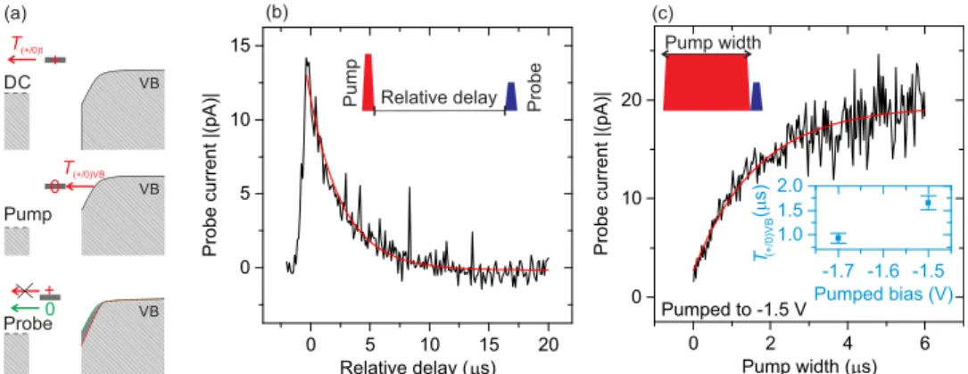
Past the NDR regime, at higher negative bias, there is a sharp turn on in current corresponding to the (+/0) level becoming resonant with the valence band.29As shown inFigure 5a, at this energy, a new filling rate (1/T(+/0)VB) from the bulk is introduced. We use an all-electronic TR-STM technique to measure this rate. The schematic inFigure 5a outlines the three elements of the experiment: the DC bias, the pump, and the probe. The DC bias is set at a value in the NDR region, and thus works to empty the DB. The pump pulse height is set to a value that pulls the (+/0) level into resonance with the valence band, serving to fill the DB. Finally, the probe is set at an energy near the valence band threshold to probe the state of the system. If the level is empty, the corresponding downward band bending from the positive charge means the probe will collect less current. If the level is neutral or full, then the VB edge at the surface will be higher, and the probe will collect more current.
The emptying rate to the tip can be measured by sweeping the relative delay between pump and probe (schematic in Figure 5b). By staying at the DC bias for longer amounts of time we measure an exponential decrease in current. The time constant associated with this decay is the emptying rate, T(+/0)t, at the valence band edge. The pump pulse must be long enough to ensure that the (+/0) level is occupied with an electron. For the data shown inFigure 5b we set the pump pulse width to 300 ns, the DC Bias to −1.2 V, the pump amplitude to −0.4 V, the probe pulse to 1 μs and the period of the pulse trains to 50 μs. The time constant we measured for the emptying rate at this energy is T(+/0)t= 2.78 ± 0.12 μs, which is consistent with our previous measurements on a 1250 °C flashed sample.
To measure the filling time constant (T(+/0)VB), we keep all parameters constant except for the pump width. For small pump widths the (+/0) level has not had the chance to be filled by valence band electrons, resulting in the probe pulse measuring less current. For larger pump widths the (+/0) level has sufficient time to be filled by the valence band, resulting in more measured current by the probe pulse. By sweeping this value and measuring probe current, we get the exponential curve shown in Figure 5c. Note that since we are changing the duration of the pump pulse, we must be careful in extracting the probe current from the averaged measured current. To do this we run two experiments. One with both the pump and probe, and one with just the pump. We then take the difference in the collected current for these measurements to extract only the probe current. The data shown inFigure 5c is the probe current only. By fitting this curve we extract the filling time constant (T(+/0)VB). The relative delay between pump and probe pulses must be constant and smaller than the emptying time of the tip. For the experimental data shown in Figure 5c we set the relative delay to 10 ns, the DC bias to −1.3 V, the probe amplitude to −0.18 V, and the period of pulse trains to 50 μs. The time constants measured for different pumped voltages are shown in the blue inset of Figure 5c. As expected, the filling rate increases with higher pump amplitude because the overlap of the (+/0) level with the valence band increases. For the experiments shown in Figure 5, a 1250 °C flashed sample was used.
Figure 4. (a, b) Symmetric properties of the rate-limited bulk-to-surface transport effect in n-type and p-type silicon, respectively. The I(V) curves comparing a DB with H−Si show the characteristic feature of NDR when the charge carriers are electrons (n-type) and also holes (p-type). Note, the graphs have been shifted to align the bulk conduction and valence band edges of both curves. The bands are hatched for clarity and the NDR onset features are marked with a black arrow for both n- and p-type.
ACS Nano Article
DOI:10.1021/acsnano.7b07068
ACS NanoXXXX, XXX, XXX−XXX
The transition levels are defined as the energy required to put additional electrons into the DB. This implies that the effective electric field at the site will energetically shift the states. The presence of any negative charge, such as another DB, will cause the transition levels and the surrounding bands to be shifted higher in energy as shown in Figure 6c. This is
intuitive since it will take more energy to add an electron to the DB if there are other negative charges in the vicinity. By adding DBs around a target DB, as illustrated inFigure 6a, we observe a consistent shift of features in the I(V) curves. The black curve in Figure 6b shows the spectroscopy of the center DB in the image ofFigure 6a before any additional DBs were added. The two surrounding DBs were sequentially placed in the order they are labeled with a corresponding I(V) taken over the probed DB after each addition.
We can understand these shifts by discussing each of its features and their relation to the newly positioned transition levels. First, the amplitude of the NDR peak decreases indicating that the conduction band is being bent upward; there are now fewer states below the Fermi level to supply the DB. The second feature is the onset of the NDR region, which shifts to a less negative bias as indicated by the vertical dashed lines marking the onset of the NDR inFigure 6b. This is due to the (+/0) level now being higher in energy, so that it can be emptied by the tip at smaller negative sample biases. In the NDR region the current tends to 0, and the DB is on average empty because the filling rates from the bulk have decreased. Finally, the post-NDR onset of the valence band current shifts to more negative bias values since the (+/0) level now requires a larger negative bias to come into resonance with the valence band. Using simple electrostatics, we estimate the electrostatic potential energy induced by each of the perturber DBs at the position of probed DB to be 45 meV. This estimate which does not include the screening effect and the tip induced band bending is in good agreement with the measured value of approximately 40 meV inFigure 6b for the energy shift of the NDR peak after addition of each perturber DB.
CONCLUSIONS
To summarize, we used the techniques of STS, KPFM, and TR-STM to examine the effect of substrate temperature, doping type, doping concentration, and electrostatic perturbation on a single DB gap state. The NDR effect originally observed with n-type samples was found to also occur for p-n-type samples under complementary conditions, which could be straightforwardly accounted for by extension of a common model. STS measurements illustrate that controlled change of the tip− sample distance allows control of the average charge state of the DB and conduction through that state. KPFM corroborates the STS study, giving the relative energetic positions of the DB’s charge transition levels. Further tuning was achieved by altering the majority carrier concentration of the system. Measurements made at higher temperature enabled thermionic carrier generation and the increase of rates. The first measurement of filling and emptying rates for the (0/+) level from the valence band have been determined. Finally, a target DB’s Figure 5. (a) Schematic showing the measurement of the filling and emptying rates of the (0/+) level from the valence band to the tip using TR-STM. DC represents the fixed bias used to empty the DB to a positive state. Pump represents the pulse bias used to fill the DB from the valence band, and probe represents the pulse bias used to sample the charge state of the DB. T(+/0)VBdenotes the time constant of electron
transition from the valence band to the (0/+) state. T(+/0)tdenotes the time constant of electron transition from the (0/+) state to the tip. (b)
Measurement of T(+/0)tby sweeping the relative delay between the pump and probe pulse. The red curve is the single exponential fit. The inset
schematically illustrates the measurement setup. (c) Measurement of T(+/0)VBby varying the pump pulse width while maintaining the probe
pulse height and relative delay constant. The blue inset is the measurement of T(+/0)VBfor different pumped biases. The red curve is the single
exponential fit. The top inset illustrates the measurement setup. For the experiments shown in (b) and (c), a 1250 °C flashed sample is used.
Figure 6. (a) STM image of the initial central DB and the two perturbing DBs. (b) The I(V) spectra of the lone central DB before (black), after the addition of perturber #1 (red), and after the addition of perturber #2 (blue). The dashed lines indicate the onset of NDR for each curve. The arrows indicate the shift of the post-NDR current onset after adding each perturber DB. (c) Energy band diagram of the system of study displaying the energy shift of (+/0), (0/−), the conduction band, and the valence band in the presence of a perturbing DB.
DOI:10.1021/acsnano.7b07068
ACS NanoXXXX, XXX, XXX−XXX
electronic character was shown to be tunable in a predictable manner through Coulombic interactions induced by the placement of negatively charged DBs nearby.
EXPERIMENTAL METHODS
These measurements were performed using an Omicron low temperature STM operated at 4.5, 77 K, and room temperature. A Nanonis SPM controller and associated software were used for data acquisition. STM tips were made of both tungsten and iridium to demonstrate our results are tip independent. Tungsten and iridium were electrochemically etched, cleaned, and sharpened by nitrogen-assisted field ion microscopy.43Boron (5−7 mΩ·cm) and arsenic (3− 4 mΩ·cm) doped Si(100) wafers were used in these experiments. The samples were degassed for several hours at 600 °C prior to hydrogen termination. The oxide layer was then desorbed by flash annealing the crystal between 1050 and 1250 °C, depending on desired dopant concentration. Hydrogen termination was done at 330 °C under exposure of H atoms for 30 s. Single DBs are created by placing the tip over a hydrogen atom at a reference height defined by 1.30 V and 50 pA and applying a positive sample voltage pulse (2.0−2.4 V) to desorb the hydrogen atom.
Radio frequency (RF) wiring with a 500 MHz bandwidth enables the STM to achieve all-electronic time-resolved measurements on the order of nanoseconds. A RF switch (Mini-Circuits ZX80-DR230-S+) was connected to each of the two output channels of an arbitrary function generator (Tektronix AFG3252C), toggling between it and ground. The outputs of the switches were fed into an adder (Mini-Circuits ZFRSC-42-S+) and connected to the tip. To account for distortion that may occur for small pulses at the junctions, cross-correlation signals were measured over H−Si to extract a proper calibration. To mitigate ringing at the junction, the pulse edges were set to 2.5 ns. In our time-resolved experiments we can vary many parameters including: pulse frequency, pulse amplitude, pulse width, and relative delay between pulse pairs from each output.
NC-AFM experiments were all carried out at 4.5 K. A Tungsten-tipped commercial (Omicron) qPlus AFM sensor with a separate tunneling wire was used to avoid cross-talk problems under bias.44The sensor exhibited a quality factor of 15k with a resonance frequency of 25 kHz. KPFM curves were taken from a fixed height with a fixed amplitude of 100 pm, calibrated using the tunnel current method.45
The tip was allowed to settle overnight before all curves were acquired to minimize piezo drift.
AUTHOR INFORMATION Corresponding Author *E-mail:[email protected]. ORCID Mohammad Rashidi: 0000-0002-8830-4812 Taleana R. Huff: 0000-0002-6876-8265 Author Contributions
∥M.R. and E.L. contributed equally to this work.
Notes
The authors declare no competing financial interest.
ACKNOWLEDGMENTS
We thank Martin Cloutier and Mark Salomons for their technical expertise as well as Leo Gross for stimulating discussions. We also thank NRC, NSERC, AITF and Compute Canada for support.
REFERENCES
(1) Morello, A.; Pla, J. J.; Zwanenburg, F. A.; Chan, K. W.; Tan, K. Y.; Huebl, H.; Möttönen, M.; Nugroho, C. D.; Yang, C.; van Donkelaar, J. A.; Alves, A. D. C.; Jamieson, D. N.; Escott, C. C.; Hollenberg, L. C. L.; Clark, R. G.; Dzurak, A. S. Single-Shot Readout of an Electron Spin in Silicon. Nature 2010, 467, 687−691.
(2) Koenraad, P. M.; Flatté, M. E. Single Dopants in Semiconductors.
Nat. Mater. 2011, 10, 91−100.
(3) Pantelides, S. T. The Electronic Structure of Impurities and Other Point Defects in Semiconductors. Rev. Mod. Phys. 1978, 50, 797−858.
(4) Shockley, W.; Read, W. T. Statistics of the Recombination of Holes and Electrons. Phys. Rev. 1952, 87, 835−842.
(5) Nunes, G.; Freeman, M. R. Picosecond Resolution in Scanning Tunneling Microscopy. Science 1993, 262, 1029−1032.
(6) Loth, S.; Etzkorn, M.; Lutz, C. P.; Eigler, D. M.; Heinrich, A. J. Measurement of Fast Electron Spin Relaxation Times with Atomic Resolution. Science 2010, 329, 1628−30.
(7) Loth, S.; Baumann, S.; Lutz, C. P.; Eigler, D. M.; Heinrich, A. J. Bistability in Atomic-Scale Antiferromagnets. Science 2012, 335, 196− 9.
(8) Grosse, C.; Etzkorn, M.; Kuhnke, K.; Loth, S.; Kern, K. Quantitative Mapping of Fast Voltage Pulses in Tunnel Junctions by Plasmonic Luminescence. Appl. Phys. Lett. 2013, 103, 183108.
(9) Jelic, V.; Iwaszczuk, K.; Nguyen, P. H.; Rathje, C.; Hornig, G. J.; Sharum, H. M.; Hoffman, J. R.; Freeman, M. R.; Hegmann, F. A. Ultrafast Terahertz Control of Extreme Tunnel Currents through Single Atoms on a Silicon Surface. Nat. Phys. 2017, 13, 591−598.
(10) Moult, I.; Herve, M.; Pennec, Y. Ultrafast Spectroscopy with a Scanning Tunneling Microscope. Appl. Phys. Lett. 2011, 98, 233103.
(11) Saunus, C.; Raphael Bindel, J.; Pratzer, M.; Morgenstern, M. Versatile Scanning Tunneling Microscopy with 120 ps time resolution.
Appl. Phys. Lett. 2013, 102, 051601.
(12) Yan, S.; Choi, D.-J.; Burgess, J. A. J.; Rolf-Pissarczyk, S.; Loth, S. Control of Quantum Magnets by Atomic Exchange Bias. Nat.
Nanotechnol. 2014, 10, 40−45.
(13) Cocker, T. L.; Jelic, V.; Gupta, M.; Molesky, S. J.; Burgess, J. a. J.; Reyes, G. D. L.; Titova, L. V.; Tsui, Y. Y.; Freeman, M. R.; Hegmann, F. a. An Ultrafast Terahertz Scanning Tunnelling Microscope. Nat. Photonics 2013, 7, 620−625.
(14) Rashidi, M.; Burgess, J. A. J.; Taucer, M.; Achal, R.; Pitters, J. L.; Loth, S.; Wolkow, R. A. Time-Resolved Single Dopant Charge Dynamics in Silicon. Nat. Commun. 2016, 7, 13258.
(15) Rashidi, M.; Vine, W.; Burgess, J. A. J.; Taucer, M.; Achal, R.; Pitters, J. L.; Loth, S.; Wolkow, R. A. All-Electronic Nanosecond-Resolved Scanning Tunneling Microscopy: Facilitating the Inves-tigation of Single Dopant Charge Dynamics. arXiv:1706.08906 2017. (16) Cocker, T. L.; Peller, D.; Yu, P.; Repp, J.; Huber, R. Tracking the Ultrafast Motion of a Single Molecule by Femtosecond Orbital Imaging. Nature 2016, 539, 263−267.
(17) Haider, M. B.; Pitters, J. L.; Dilabio, G. A.; Livadaru, L.; Mutus, J. Y.; Wolkow, R. A. Controlled Coupling and Occupation of Silicon Atomic Quantum Dots at Room Temperature. Phys. Rev. Lett. 2009,
102, 046805.
(18) Huff, T.; Labidi, H.; Rashidi, M.; Achal, R.; Livadaru, L.; Dienel, T.; Pitters, J.; Wolkow, R. A. Binary Atomic Silicon Logic.
arXiv:1706.07427 2017.
(19) Kolmer, M.; Zuzak, R.; Dridi, G.; Godlewski, S.; Joachim, C.; Szymonski, M. Realization of a Quantum Hamiltonian Boolean Logic gate on the Si(001):H Surface. Nanoscale 2015, 7, 12325−12330.
(20) Livadaru, L.; Xue, P.; Shaterzadeh-Yazdi, Z.; DiLabio, G. a.; Mutus, J.; Pitters, J. L.; Sanders, B. C.; Wolkow, R. a. Dangling-Bond Charge Qubit on a Silicon Surface. New J. Phys. 2010, 12, 083018.
(21) Kolmer, M.; Godlewski, S.; Zuzak, R.; Wojtaszek, M.; Rauer, C.; Thuaire, A.; Hartmann, J. M.; Moriceau, H.; Joachim, C.; Szymonski, M. Atomic Scale Fabrication of Dangling Bond Structures on Hydrogen Passivated Si(0 0 1) Wafers Processed and Nanopackaged in a Clean Room Environment. Appl. Surf. Sci. 2014, 288, 83−89.
(22) Møller, M.; Jarvis, S. P.; Guérinet, L.; Sharp, P.; Woolley, R.; Rahe, P.; Moriarty, P. Automated Extraction of Single H Atoms with STM: Tip State Dependency. Nanotechnology 2017, 28, 075302.
(23) Soukiassian, L.; Mayne, A. J.; Carbone, M.; Dujardin, G. Atomic-Scale Desorption of H Atoms from the Si(100)-2 × 1:H Surface: Inelastic Electron Interactions. Phys. Rev. B: Condens. Matter Mater.
Phys. 2003, 68, 035303.
ACS Nano Article
DOI:10.1021/acsnano.7b07068
ACS NanoXXXX, XXX, XXX−XXX
(24) Huff, T. R.; Labidi, H.; Rashidi, M.; Koleini, M.; Achal, R.; Salomons, M. H.; Wolkow, R. A. Atomic White-Out: Enabling Atomic Circuitry through Mechanically Induced Bonding of Single Hydrogen Atoms to a Silicon Surface. ACS Nano 2017, 11, 8636−8642.
(25) Pavliček, N.; Majzik, Z.; Meyer, G.; Gross, L. Tip-Induced Passivation of Dangling Bonds on Hydrogenated Si(100)-2 × 1. Appl.
Phys. Lett. 2017, 111, 053104.
(26) Schofield, S. R.; Studer, P.; Hirjibehedin, C. F.; Curson, N. J.; Aeppli, G.; Bowler, D. R. Quantum Engineering at the Silicon Surface Using Dangling Bonds. Nat. Commun. 2013, 4, 1649.
(27) Berthe, M.; Stiufiuc, R.; Grandidier, B.; Deresmes, D.; Delerue, C.; Stiévenard, D. Probing the Carrier Capture Rate of a Single Quantum Level. Science 2008, 319, 436−438.
(28) Nguyen, T. H.; Mahieu, G.; Berthe, M.; Grandidier, B.; Delerue, C.; Stiévenard, D.; Ebert, P. Coulomb Energy Determination of a Single Si Dangling Bond. Phys. Rev. Lett. 2010, 105, 226404.
(29) Rashidi, M.; Taucer, M.; Ozfidan, I.; Lloyd, E.; Koleini, M.; Labidi, H.; Pitters, J. L.; Maciejko, J.; Wolkow, R. A. Time-Resolved Imaging of Negative Differential Resistance on the Atomic Scale. Phys.
Rev. Lett. 2016, 117, 276805.
(30) Esaki, L. New Phenomenon in Narrow Germanium p-n Junctions. Phys. Rev. 1958, 109, 603−604.
(31) Labidi, H.; Taucer, M.; Rashidi, M.; Koleini, M.; Livadaru, L.; Pitters, J.; Cloutier, M.; Salomons, M.; Wolkow, R. a. Scanning Tunneling Spectroscopy Reveals a Silicon Dangling Bond Charge State Transition. New J. Phys. 2015, 17, 073023.
(32) Taucer, M.; Livadaru, L.; Piva, P. G.; Achal, R.; Labidi, H.; Pitters, J. L.; Wolkow, R. A. Single-Electron Dynamics of an Atomic Silicon Quantum Dot on the H-Si(001)-(2 × 1) Surface. Phys. Rev.
Lett. 2014, 112, 256801.
(33) Berthe, M.; Urbieta, A.; Perdigão, L.; Grandidier, B.; Deresmes, D.; Delerue, C.; Stiévenard, D.; Rurali, R.; Lorente, N.; Magaud, L.; Ordejón, P. Electron Transport via Local Polarons at Interface Atoms.
Phys. Rev. Lett. 2006, 97, 206801.
(34) Steurer, W.; Repp, J.; Gross, L.; Scivetti, I.; Persson, M.; Meyer, G. Manipulation of the Charge State of Single Au Atoms on Insulating Multilayer Films. Phys. Rev. Lett. 2015, 114, 036801.
(35) Steurer, W.; Fatayer, S.; Gross, L.; Meyer, G. Probe-Based Measurement of Lateral Single-Electron Transfer Between Individual Molecules. Nat. Commun. 2015, 6, 8353.
(36) Wagner, C.; Green, M. F.; Leinen, P.; Deilmann, T.; Krüger, P.; Rohlfing, M.; Temirov, R.; Tautz, F. S. Scanning Quantum Dot Microscopy. Phys. Rev. Lett. 2015, 115, 026101.
(37) Stomp, R.; Miyahara, Y.; Schaer, S.; Sun, Q.; Guo, H.; Grutter, P.; Studenikin, S.; Poole, P.; Sachrajda, A. Detection of Single-Electron Charging in an Individual InAs Quantum Dot by Noncontact Atomic-Force Microscopy. Phys. Rev. Lett. 2005, 94, 056802.
(38) Kocić, N.; Decurtins, S.; Liu, S. X.; Repp, J. Forces from Periodic Charging of Adsorbed Molecules. J. Chem. Phys. 2017, 146, 092327.
(39) Kocić, N.; Weiderer, P.; Keller, S.; Decurtins, S.; Liu, S. X.; Repp, J. Periodic Charging of Individual Molecules Coupled to the Motion of an Atomic Force Microscopy Tip. Nano Lett. 2015, 15, 4406−4411.
(40) Konig, T.; Simon, G. H.; Rust, H.-P.; Pacchioni, G.; Heyde, M.; Freund, H.-J. Measuring the Charge State of Point Defects on MgO/ Ag (001). J. Am. Chem. Soc. 2009, 131, 17544−17545.
(41) de la Broïse, X.; Delerue, C.; Lannoo, M.; Grandidier, B.; Stiévenard, D.; de la Broise, X.; Delerue, C.; Lannoo, M.; Grandidier, B.; Stievenard, D. Theory of Scanning Tunneling Microscopy of Defects on Semiconductor Surfaces. Phys. Rev. B: Condens. Matter
Mater. Phys. 2000, 61, 2138−2145.
(42) Pitters, J. L.; Piva, P. G.; Wolkow, R. A. Dopant Depletion in the Near Surface Region of Thermally Prepared Silicon (100) in UHV. J.
Vac. Sci. Technol., B: Nanotechnol. Microelectron.: Mater., Process., Meas., Phenom. 2012, 30, 021806.
(43) Rezeq, M.; Pitters, J.; Wolkow, R. Tungsten Nanotip Fabrication by Spatially Controlled Field-Assisted Reaction with Nitrogen. J.
Chem. Phys. 2006, 124, 204716.
(44) Majzik, Z.; Setvín, M.; Bettac, A.; Feltz, A.; Cháb, V.; Jelínek, P. Simultaneous Current, Force and Dissipation Measurements on the Si(111) 7 × 7 Surface with an Optimized qplus AFM/STM Technique. Beilstein J. Nanotechnol. 2012, 3, 249−259.
(45) Simon, G. H.; Heyde, M.; Rust, H. Recipes for Cantilever Parameter Determination in Dynamic Force Spectroscopy: Spring Constant and Amplitude. Nanotechnology 2007, 18, 255503.
DOI:10.1021/acsnano.7b07068
ACS NanoXXXX, XXX, XXX−XXX