HAL Id: cea-02421723
https://hal-cea.archives-ouvertes.fr/cea-02421723
Submitted on 18 Feb 2020
HAL is a multi-disciplinary open access archive for the deposit and dissemination of sci-entific research documents, whether they are pub-lished or not. The documents may come from teaching and research institutions in France or abroad, or from public or private research centers.
L’archive ouverte pluridisciplinaire HAL, est destinée au dépôt et à la diffusion de documents scientifiques de niveau recherche, publiés ou non, émanant des établissements d’enseignement et de recherche français ou étrangers, des laboratoires publics ou privés.
Development of a tip enhanced near-field laser ablation
system for sub-micrometric analysis of solid samples
Chirelle Jabbour, Jean-Luc Lacour, Michel Tabarant, Alexandre Semerok,
Fredéric Chartier
To cite this version:
Chirelle Jabbour, Jean-Luc Lacour, Michel Tabarant, Alexandre Semerok, Fredéric Chartier. Develop-ment of a tip enhanced near-field laser ablation system for sub-micrometric analysis of solid samples. Journal of Analytical Atomic Spectrometry, Royal Society of Chemistry, 2016, 31, pp.1534-1541. �10.1039/C6JA00044D�. �cea-02421723�
1
Influence of the laser wavelength on tip-enhanced near-field laser
ablation of solid samples
C.Jabbour1,*, A. Semerok1, J-L. Lacour1, M. Tabarant1, S. V. Fomichev2, 3, J. Moryousef1, J. Simonnet1, 4 and F. Chartier1, 5, *
1DEN-DANS-Service d’Etudes Analytiques et de Réactivité des Surfaces (SEARS), CEA, Université Paris-Saclay,
F-91191 Gif-sur-Yvette, France
2National Research Center “Kurchatov Institute”, 123182 Moscow, Russia
3Moscow Institute of Physics and Technology, 141700 Dolgoprudny, Moscow region, Russia 4Sorbonne Universités, UPMC Université Paris 06, 75252 Paris cedex 05, France
5DEN-DANS-Département de Physico-Chimie, Direction, CEA, Université Paris-Saclay, F-91191 Gif-sur-Yvette,
France
*Corresponding authors’ email addresses: [email protected] [email protected]
Abstract
We have studied the influence of the laser wavelength (266 nm and 532 nm) on the tip-enhanced near-field laser ablation of conducting gold and semiconducting silicon samples. The near-field laser ablation effect was obtained by coupling a nanosecond Nd:YAG laser to an atomic force microscope. Experiments were carried out at atmospheric pressure with one and multiple laser pulses. The near-field ablation showed distinct differences in the dimensions of the craters according to the laser wavelength and the nature of the sample. On gold samples, with the same number of laser pulses, larger craters were obtained at 532 nm while the crater depths remained almost constant for both wavelengths. On silicon samples and under the same experimental conditions, craters were only obtained at 266 nm, while at 532 nm no defined structure was observed below 200 laser pulses. These experimental results were in accordance with the numerical simulations of the localized heating given by a home-made 3D code. Both the experimental and theoretical approaches showed that the sample absorption coefficient set by the laser wavelength was one of the most important parameters affecting the efficiency of the near-field laser ablation.
2
Introduction
Local analysis and chemical characterization of solid samples with sub-micrometer resolution are gaining importance in many scientific fields such as materials research, biology, geology, etc [1-4]. Over the years, near-field laser ablation (NF-LA) has demonstrated that it is a powerful solid sampling technique at the nanometer scale [5-6]. In comparison with conventional laser ablation (LA), the major advantage of NF-LA is its ability to overcome the optical diffraction limit, which is impossible with traditional laser ablation.
Laser ablation is a convenient and widespread solid sampling technique applied on a large range of conducting and non-conducting samples. In order to perform quantitative analysis, a laser beam is usually coupled to emission or mass spectrometric techniques (laser-induced breakdown spectroscopy (LIBS), laser ablation inductively coupled plasma with optical emission spectrometry or with mass spectrometry (LA-ICP-OES/-MS)). The usual spatial resolution of LA analysis techniques is in the range of 5 – 300 μm [5]. The best-achieved resolutions were found in the range of a few micrometers (2 – 3 μm) [7-8]. Despite the fact that such a resolution ensures the analysis of a large range of solid samples, extending the spatial resolution is of great importance to analyze fine structures and small zones of solid samples and it explains the development of NF-LA during the past few years.
Guided through an etched optical fiber (NF-LA aperture configuration) [6, 9] or illuminating the extremity of a sharp, pointed tip (NF-LA apertureless configuration) [5, 10], the laser field can be locally confined on a very small interaction spot comparable with the fiber/tip radius, i.e., from a few tens to a few hundreds of nanometers. Both the etched optical fiber and the sharp pointed tip are maintained a few nanometers above the sample surface. The local confinement of laser radiation leads to the near-field ablation and generates craters whose diameters are of the same order of magnitude as the fiber/tip diameter. In the apertureless configuration used in the present study, the ablation efficiency depends on the tip parameters (nature, dimension and tip-to-sample distance), the laser parameters (fluence and polarization) and the sample nature and properties [11]. The reduction of the ablation spot to a few tens of nanometers, while improving
3
the resolution, also leads to the generation of a very small quantity of ablated matter. Any coupling with this sampling technique will therefore require a highly sensitive technique for chemical characterization such as ICP-MS.
The optimization of spatial resolution and ablation efficiency, in order to form as much ablated mass as possible for chemical characterization, turns the choosing of laser parameters into a critical task for micro- and nano-analysis. Many studies on direct laser ablation have been reported in the literature [12-15]. Among the studied parameters, the laser wavelength is a fundamental one affecting the laser-matter interaction. On the one hand, depending on the sample target, the laser wavelength determines the optical penetration depth and the distribution of light intensity as a function of depth: the laser energy may remain on the sample surface or propagate through the sample [16-17]. On the other hand, the laser wavelength is of great importance for the LIBS technique performance because it affects the plasma behavior and its temporal evolution [18-19]. In this case, it should be noted that the plasma expansion also depends on the laser pulse duration and on the size of the laser interaction spot [20-21].
The effect of the wavelength on the size and shape of the craters as well as on the ablation efficiency of AL has been extensively studied [12, 19, 22-25]. For example, Torrisi et al. [22] studied three different wavelengths: 1064 nm and 532 nm emitted by an Nd:YAG laser and 248 nm delivered by a KrF laser. At a fluence of 4 J.cm-², the craters obtained on PMMA polymer during infrared (IR) and visible laser ablation were large with a rough edge containing re-solidified ablated material whereas the craters obtained with UV light (248 nm wavelength) showed a very neat edge. The authors explained this observation with the difference in ablation process: longer wavelengths, i.e., IR and visible, mainly involved a photo-thermal ablation process whereas shorter wavelengths, i.e., UV, induced photochemical mechanisms.
On copper samples, Geertsen et al. [23] studied the laser ablation efficiency as a function of the laser wavelength. Three laser sources were employed: an Nd:YAG laser operating at 1064 nm, 532 nm and 355 nm and two excimer lasers, XeCl and ArF, emitting at 308 nm and 193 nm, respectively. The authors showed that the ablation efficiency was about 20 and 10 times higher
4
for a UV laser than for respectively an IR and visible laser: at a fluence of 200 J.cm-², a mass of about 60 µg of copper was ablated at 193 nm, for example. The authors explained that, for UV wavelengths, direct laser ablation was the major process responsible for the material removal, while with IR and visible laser radiation, the produced plasma acted as a shield for the incoming radiation and less laser energy interacted directly with the sample surface thus limiting the ablation performance.
The same observation was made by Semerok et al. [19] who compared the ablation efficiency at different pulse durations and wavelengths. For example, for a fluence of 650 J.cm-2 and ps pulses, the authors measured crater depths of 2 μm and 7 μm for a wavelength of 532 nm and 266 nm, respectively, on copper samples. They concluded that, for ns and ps laser pulses, the ablation efficiency was 2 to 3 times higher at UV wavelengths than at visible radiation. A similar conclusion was made by Hussein et al. [24] who studied the laser wavelength effect on an aluminum target: with an Nd:YAG nanosecond laser, the authors showed that the measured crater depths increased when decreasing the laser wavelength. With the same fluence of 318 J.cm-², the crater depth decreased from 33 µm to approximately 5 µm as the laser wavelength increased from 266 nm to 1064 nm. According to the authors, the strong plasma produced at long wavelengths prevented the direct laser-target interaction.
Russo et al. [12] studied the influence of three wavelengths in the UV spectral region on glass samples with different opacity. The wavelengths were emitted by an F2 excimer laser (157 nm) and two Nd:YAG lasers (213 nm and 266 nm), operating with an energy maintained at 0.8 mJ. The authors showed that the shorter the wavelength, the more reproducible was the ablation rate and the more reduced was the matrix dependence. In another study by the same group, Gonzalez et al. [25] showed that after 40 pulses on a NIST 610 glass, the 266 nm wavelength produced deep craters (35 nm) while shallower and flatter craters (8-15 nm) were obtained for 213 and 193 nm. The ablation rate (defined as the obtained crater depth per pulse) was greater at 266 nm. It should be noted here that the opacity of the glass samples is highly dependent on the laser wavelength and affects the optical penetration depth of each sample [12, 25].
5
In general, depending on the laser wavelength, the laser ablation process may induce thermal and/or non-thermal mechanisms [26]. The IR wavelength involves mainly a thermal effect (heating, melting, vaporization…) while the UV wavelength induces primarily a photochemical effect due to the high photon energy. In this case, when the photon energy is higher than the chemical energy of the bonding of the target atoms, the laser can break these chemical bonds and release molecular, atomic and ionic species [22]. Despite it being difficult to isolate the influence of the laser wavelength on the ablation behavior from the influence of other important parameters such as the laser pulse duration, the laser energy or the sample properties, it has been shown that the shorter the laser wavelength, the higher the ablation rate [26].
Several NF-LA applications have been explored, with [27-28] or without [29-30] chemical analysis of solid samples. However, unlike conventional laser ablation studies, the laser wavelength effect on the near-field ablation efficiency and on the crater dimensions has not been widely studied. Zorba et al. [2, 9] explored the influence of the laser wavelength on crater dimensions during nanostructuring of silicon wafer samples with an aperture NF-LA configuration. A Ti:Sapphire laser (100 fs, 10 Hz) emitting two wavelengths (λ = 400 nm and the fundamental wavelength λ = 800 nm) was coupled to a sub-wavelength SNOM fiber probe aperture (100-150 nm). Distinct differences in the crater structures were observed depending on laser wavelength: on silicon samples, nanometer craters were only observed at a 400 nm wavelength. With this wavelength, the diameters of the obtained craters at full-width at half maximum (FWHM) ranged from 27 nm to 550 nm for 1 to 500 pulses, respectively. Under these conditions, 1.2 nm deep craters to 52 nm high “protrusions” were obtained. With the fundamental laser wavelength of 800 nm, only protrusions were observed independently of the number of laser pulses. In this case, the diameters of the protrusions at FWHM ranged from 90 nm to 760 nm for 5 to 500 pulses, respectively, and their height remained stable around 1 nm. No protrusions were seen with a single laser pulse at 800 nm. According to the authors, the absorption of the laser light by the material for each wavelength is an important factor that should be considered. Assuming linear absorption, the optical penetration depth for Si varied from 164 nm to 25 µm for the 400 and 800 nm irradiation wavelengths, respectively. Based on a simple thermal energy model, authors
6
showed that the deposited energy per volume of material differed significantly between the two wavelengths and led to a higher temperature of the Si sample at 400 nm (170 000 K) than at 800 nm (1 800 K). According to the authors, these differences were responsible for the ‘’more ablative’’ behavior at 400 nm. At 800 nm, the ablation behavior appeared to be a material melting process since the melting point of Si is around 1 700 K.
In a previous work [11], a multiparametric study (tip nature and dimension, tip-to-sample distance, laser fluence, sample nature) on tip-enhanced NF-LA was carried out in order to identify the effect of these parameters on the dimensions of the produced craters, the lateral resolution and the amount of ablated material. In order to develop this work further, the effect of the laser wavelength on the near-field ablation efficiency and on the crater dimensions was studied for two different types of solid samples: gold and silicon. With an apertureless configuration and a nanosecond laser, both experimental and theoretical approaches are discussed herein.
Experimental section
Materials and methods
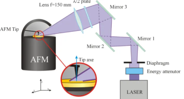
To perform tip-enhanced near-field laser ablation, the instrumentation was constituted by a combination of a nanosecond laser and an atomic force microscope. An Nd:YAG laser (Minilite Continuum, Santa Clara, California, USA) was used as the irradiation source, delivering 4 ns pulses with a repetition rate of 10 Hz. Both frequency-doubled (532 nm) and -quadrupled (266 nm) laser wavelengths were used. A tip from a Nano-Observer (CSI, Scientec, Les Ulis, France) atomic force microscope (AFM) was utilized to ensure the near-field tip-enhancement effect above the sample surface. In addition, the AFM provided the topographic information before and after the ablation in order to characterize the obtained craters. Conductive diamond-coated silicon AFM tips (NanoAndMore, Wetzlar, Germany) with a diameter of 200-250 nm were used in this study. A scheme of the experimental setup is shown in Figure 1. The AFM tip was illuminated by the laser beam passing through a laser energy attenuator, a diaphragm, 3 mirrors, a half-wavelength plate and a focusing lens. The tip axis was parallel to the laser’s incident plane and perpendicular to
7
the sample surface. For both wavelengths, the laser field was guided through the same experimental setup and the appropriate optics for each wavelength were used.
In our setup, due to the mechanical design of the AFM, the laser beam was delivered with an inclination angle of 70° to the tip axis. The mirrors and the focusing lens made it possible to align and to illuminate the tip with a laser fluence below the ablation thresholds of the sample and of the tip. To control the size of the interaction laser spot with the tip, a top-hat laser beam was provided by diaphragm imaging on the tip apex. The tip was immersed in a laser spot with a diameter of about 300 µm. This laser interaction spot made it possible to control the tip illumination and the homogeneity of the fluence. Moreover, the match between the polarization direction and the tip axis was important for a large enhancement in the near-field of a tip [31]. Consequently, a half-wavelength plate was set in front of the lens to ensure a p-polarized laser radiation that was parallel to the incident plane.
Fig. 1: Schematic experimental setup.
Sample preparation
In order to study the laser wavelength effect on the near-field laser ablation efficiency, two types of samples were used in our experiments: a conducting sample of gold and a semi-conducting silicon wafer sample. The aim of using these two sample types was to compare their behavior against laser heating at both wavelengths and to observe the impact of oxidation which may occur with silicon in air at atmospheric pressure. Ionic polishing was applied to the samples to reduce most of the surface defects and to ensure a nanometric surface roughness.
8
Measurement procedure
The sample was placed on the AFM piezo manipulator, movable in the vertical direction. Using an AFM allows to precisely control the tip position over the sample surface. However, the AFM tip cannot be maintained in a static state during the ablation time. In order to generate craters with multiple laser pulses, the tip scans a very small area of 5 nm that can be considered as a fixed tip position above the sample surface. Each line of this scan is performed in two passes. The first one is carried out in contact mode and the line topography is saved. During the second pass, the tip follows the same memorized line topography but while lifted above the sample surface at a distance of a few nanometers, controlled by the operator and kept constant during the whole experiment. The Nd:YAG laser was synchronized with the displacement of the tip. The tip was illuminated only during the second pass. By illuminating the tip apex with the laser beam, the laser radiation was confined to the immediate tip vicinity and locally enhanced on a few tens of nanometers of the sample surface, leading to near-field laser ablation.
The AFM was then used to make a precise cartography of the craters formed by near-field ablation. These cartographies were made using contact mode, on micrometric square areas. In this work, all measurements were carried out at an ambient temperature, in air at atmospheric pressure.
Results and discussions
On the same experimental setup, the multiparametric study already carried out [11] made it possible to identify the influence of the following experimental parameters on the laser ablation efficiency and the amount of ablated mass: tip nature, tip dimension, tip-to-sample distance, laser fluence and number of laser pulses. In short, it has been shown that the tip-enhanced near-field effect of a laser radiation of 80 mJ.cm-2 produced by a conductive tip maintained 5 nm above the surface of a conducting sample ensured the best ablation yield and the largest amount of ablated mass. Based on these results, the values of the experimental parameters leading to the most effective ablation were verified for the two tested laser wavelengths: 266 and 532 nm. For a single laser pulse and for each wavelength, the largest amount of ablated mass was obtained
9
by setting the appropriate parameters to the values obtained during the previous multiparametric study.
IR radiation was not tested since the properties of the samples studied in this work, i.e., gold and silicon, are not suitable for significant observations at 1064 nm. Indeed, Si shows a very poor absorption of the laser energy at this wavelength (absorption coefficient α ≈ 2 cm-1 at 1064 nm [32-33]). Concerning Au, the thermal model (presented below) shows very restrictive conditions on the Si tip geometry in order to achieve near-field ablation at 1064 nm.
Gold sample
Gold crater diameters for the two wavelengths: Experiments were carried out on a gold sample
for a single and multiple laser pulses. Figure 2 shows crater diameters as a function of the number of laser pulses for two laser wavelengths.
Fig. 2. Crater diameter at FWHM on a gold sample as a function of the number of laser pulses with the two laser
wavelengths 266 and 532 nm. The error bars for the crater diameter correspond to a relative standard deviation at k = 1 of about 5 % for four different measurements. The dotted lines are a guide to the eye.
Experiments showed that the crater diameter at FWHM increased with the number of laser pulses. With the same number of laser pulses on the gold sample, the crater diameters obtained at 532 nm were larger than those obtained at 266 nm except for the crater obtained with a single laser pulse. At 266 nm, the crater diameter at FWHM increased from 60 nm for a single laser pulse to 230 nm for 200 laser pulses. On the other hand, at 532 nm, the gold crater diameter increased from 60 nm for a single laser pulse to about 280 nm for 200 laser pulses. The difference in diameter between the two wavelengths was about 50 nm for multi-pulse ablation.
0 50 100 150 200 250 300 350 0 50 100 150 200 250 Cr at er dia m et er a t F W HM (nm )
Number of laser pulses
Gold
532 nm 266 nm
10
In our case, with an apertureless configuration of NF-LA, when the laser light illuminated the sharp tip, the latter acted as an optical antenna producing a strong enhancement of the radiation intensity at the apex [34]. It is important to note that different mechanisms may take place under the tip and lead to sample patterning/ablation at the nanometer scale. When the laser beam is focused on the apex of a sharp tip, a high local electrical field is generated by different sources: the dipole effect, the “lightning rod” effect which depends on the geometry of sharply pointed metal structures, and the resonant plasmon effect which is related to the laser wavelength and the tip geometry.
According to Lu et al. [35] who carried out a theoretical study of the electric field distribution of the laser radiation on a gold sample beneath a silver tip, the electric field intensity in the near-field region was frequency-dependent. With the increase of the laser wavelength, the authors showed that the near-field zone expanded. In the same way, Chimmalgi et al. [36] demonstrated that the enhancement factor of the electric field induced by a silicon AFM tip above thin gold films deposited on a silicon substrate increased with the laser wavelength. This enhancement factor increased from 40 to 150 when the wavelength of a femtosecond laser increased from 400 to 800 nm. According to the authors, this difference could be attributed to the fact that the antenna effect exhibited by the tip in an apertureless configuration is less dominant at visible wavelengths and prevalent at longer wavelengths. These differences of the electric field distribution beneath the tip may be one of the reasons that larger gold craters were obtained during NF-LA when the laser wavelength increased from 266 to 532 nm.
Gold crater depths for the two wavelengths: In the same way as for the crater diameters, the
crater depths were examined as a function of the number of laser pulses and the laser wavelength. The results are shown in Figure 3.
11
Fig. 3. Crater depth on a gold sample as a function of the number of laser pulses with the two laser wavelengths:
266 and 532 nm. The error bars for the crater depth correspond to a relative standard deviation at k = 1 of about 5 % for four different measurements. The dotted lines are a guide to the eye.
Experiments showed that the crater depth increased from approximately 8 nm for a single laser pulse to 125 nm after 400 pulses for both wavelengths. Beyond 400 laser pulses, the depth remained almost constant at approximately 125 nm regardless of the number of laser pulses. However, many reasons could be at the origin of the constant value of the crater depth obtained beyond 400 laser pulses. Before ablation, the tip was maintained 5 nm above the sample surface. With the operating properties of our AFM and due to the synchronization between the laser and the AFM, a maximum number of 40 pulses could be delivered by one set of pulses. The duration of one set was 4 seconds. In order to cumulate 400 laser pulses, 10 sets of 40 laser pulses each had to be delivered for the same position of the tip above the sample surface. After each pulse set, a crater was obtained which means that, during the pulse sets, the distance between the tip and the sample became more and more significant, thus reducing the near-field effect and limiting the crater depth. For a tip-to-sample distance above 30 nm, the near-field effect was significantly reduced [31]. Moreover, after the ablation, the tip scanned the surface topography
12
in order to characterize the obtained crater. With deep craters (depth > 100 nm), due to the tip and crater geometries, it was possible that the tip of the AFM could not reach the bottom of the crater and, therefore, could not measure the exact crater depth. The combination of these phenomena could lead to this seemingly constant value of the crater depth beyond 400 laser pulses.
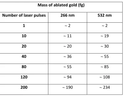
Mass of ablated gold for the two wavelengths: The influence of the laser wavelength on the
ablated mass could be studied with the obtained craters. The amount of ablated material produced by near-field laser ablation is of great analytical importance. The ablated particles will be transported to an ICP-MS in order to perform elemental qualitative and quantitative analyses. At this scale, the real shape of the crater is not exactly known and could vary between a cone and a cylinder shape. The ablated mass estimations were based on a cylindrical crater shape also used by other groups [3, 37]. The amount of ablated gold for both wavelengths is reported in Table 1.
Table 1. Mass of ablated gold for both wavelengths as a function of the number of laser pulses. The results
uncertainty was evaluated at around 10 %.
Mass of ablated gold (fg)
Number of laser pulses 266 nm 532 nm
1 ~ 2 ~ 2 10 ~ 11 ~ 19 20 ~ 20 ~ 30 40 ~ 36 ~ 55 80 ~ 55 ~ 85 120 ~ 94 ~ 108 200 ~ 190 ~ 234
The ablated mass increased from about 2 fg for a single laser pulse to about 190 fg for 200 laser pulses at 266 nm. At the wavelength of 532 nm, the amount of ablated mass was higher: the mass of ablated gold increased from approximately 2 fg for one pulse to about 230 fg for 200
13
pulses. For a single laser pulse, the crater diameters for both wavelengths were approximately the same.
To summarize the results obtained on gold, NF-LA showed nanometric craters for both wavelengths. Both the depth and the diameter of the craters increased with the number of laser pulses. The craters obtained with 532 nm were larger than those obtained with the 266 nm wavelength but the depths were similar at the two different wavelengths. It is important to keep in mind that, in the case of gold, the optical penetration depth did not vary significantly between the two wavelengths: about 13 nm for the 266 nm wavelength and 20 nm for the 532 nm wavelength [32]. In order to understand the similitude between the crater depths at both wavelengths and determine whether this behavior was associated with the sample’s optical properties, the same experiments were carried out on silicon, since this sample has very different optical properties at these wavelengths.
Silicon sample
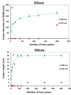
Experiments on silicon samples were carried out for a single and multiple laser pulses at the two wavelengths: 266 nm and 532 nm. Figure 4 shows the AFM cartographies of the silicon surface after near-field ablation by 40 laser pulses with a fluence maintained at 80 mJ.cm-2, which was lower than the Si ablation thresholds for 266 and 532 nm [11].
14
Fig 4. Near-field laser ablation of a silicon sample with different wavelengths (λ = 266 and 532 nm) after 40 laser pulses. Laser
fluence Flaser = 80 mJ.cm-2.
As can be seen in Figure 4, after 40 laser pulses, craters were only observed at a wavelength of 266 nm. No craters were observed at 532 nm. The diameters and depths of the obtained craters as functions of the number of laser pulses for the two wavelengths are shown in Figure 5.
Fig 5. a) Crater diameter at FWHM and b) crater depth for silicon sample as a function of the number of laser pulses with the two
laser wavelengths: 266 and 532 nm. The error bars for the crater depths/diameters correspond to a relative standard deviation at k = 1 of about 5 % for four different measurements. The dotted lines are a guide to the eye.
Silicon crater dimensions for the two wavelengths: At 266 nm, the silicon crater diameter
increased from 50 nm for a single laser pulse to about 230 nm after 200 laser pulses (Fig.5.a) and the depth increased from 4 nm for a single laser pulse to 18 nm after 80 laser pulses (Fig.5.b). At 532 nm, no craters were observed below 200 laser pulses. However, after 200 laser pulses, a small crater could be seen and it presented a diameter at FWHM of about 100 nm with a depth of 2 nm. The crater size did not show any significant evolution when increasing the number of laser pulses. These results were in accordance with the behavior of silicon during NF-LA observed by Zorba et al. [9]. As mentioned in the introduction, with a femtosecond laser, the authors
15
observed nanometer craters only at 400 nm while small protrusions were observed at 800 nm. These differences were attributed to the way that laser irradiation was absorbed by the silicon for each wavelength. Thus, due to the significant difference in optical penetration depths (164 nm and 25.5 μm for the 400 and 800 nm wavelengths, respectively) and to the consecutive density of the deposited energy, the silicon temperature was much higher at 400 nm (170 000 K) than at 800 nm (1 800 K). For the authors, this temperature difference was responsible for the ablation mechanism and the crater formation at 400 nm while only a material melting process was observed at 800 nm.
In our case, the absorption coefficients of Si varied between 209 µm-1 and 1 µm-1 when the laser wavelength increased from 266 nm to 532 nm. In other terms, the optical penetration depth for silicon increased from about 5 nm at 266 nm to 1 µm at 532 nm [33], which induced a difference in the density of the deposited energy and a lower ablation efficiency at 532 nm in comparison with 266 nm. This difference is discussed in detail below with a laboratory-made numerical code for the calculation of the heating temperature distribution. This code showed that the absorption coefficient effect on NF-LA was largely predominant over other parameters such as the laser pulse duration.
After 200 laser pulses, small craters were observed at a wavelength of 532 nm (Fig.5.a and b). The dimensions of these craters remained constant up to 600 laser pulses. It is important to note that by increasing the number of laser pulses, the sample properties were likely to change and a silicon oxide layer could be formed since the ablation was carried out in air [38-39]. This could be the origin of the observed crater formations on silicon after 200 laser pulses with a wavelength of 532 nm.
Comparison between gold and silicon ablation at λlaser = 266 nm: By increasing the number of laser pulses at 266 nm, the depth of the silicon craters increased from 4 nm for a single laser pulse to 18 nm after 80 pulses (Fig.5.b). Beyond 80 laser pulses, the crater depth remained almost constant at 18 nm. Under the same experimental conditions, the significant difference of the crater depth between gold (29 nm for 80 pulses, Fig.3) and silicon (18 nm for 80 pulses, Fig.5.b)
16
can be related to the sample’s electrical conductivity affecting the near-field tip enhancement factor. Both the thermal and electrical conductivities were greater for gold than for the silicon wafer [32], which resulted in a more effective ablation and deeper craters on the gold sample. Moreover, among the hypotheses that could explain the constant value of the silicon crater depth just beyond 80 laser pulses can be mentioned the formation of an oxide layer in an ambient atmosphere. The laser-heated area could chemically react with the oxygen in air and this reaction led to the formation of silicon oxides layer. These results were found by Mai et al. [39] during their study on a laser-induced nano-modification on a silicon surface beneath an STM tip in ambient air.
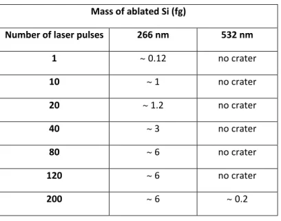
Mass of ablated silicon for the two wavelengths: As for gold, based on the approximation of a
cylindrical shape of the craters, the amount of ablated silicon as a function of the number of laser pulses at the two wavelengths is reported in Table 2.
Table 2. Mass of ablated silicon for the two wavelengths as a function of the number of laser pulses. The results uncertainty was evaluated at around 10 %.
Mass of ablated Si (fg)
Number of laser pulses 266 nm 532 nm
1 ~ 0.12 no crater 10 ~ 1 no crater 20 ~ 1.2 no crater 40 ~ 3 no crater 80 ~ 6 no crater 120 ~ 6 no crater 200 ~ 6 ~ 0.2
At 266 nm, the amount of ablated material increased from 0.12 fg for a single laser pulse to about 6 fg after 200 pulses. At 532 nm, and due to the absence of a defined crater structure, a small amount corresponding to 0.2 fg of ablated mass could be obtained after 200 laser pulses. With
17
200 laser pulses, one could notice the significant difference of ablated mass between gold (Table 1) and silicon: 190 fg of gold for 6 fg of silicon at 266 nm wavelength and 230 fg of gold for only 0.2 fg of silicon at 532 nm. This confirms that near-field laser ablation was more efficient on a conductive sample that ensures a higher ablation rate in comparison with a semi-conductive one.
Comparison of NF-LA for the two wavelengths by using a thermal model of laser heating
To understand the results obtained with the Au- and Si-samples during NF-LA for the two wavelengths (266 nm and 532 nm), one may apply a one-temperature thermal model of the laser heating of solid samples [40]:
𝐶𝐶(𝑇𝑇)𝑑𝑑𝑑𝑑𝑑𝑑𝑑𝑑 = 𝑑𝑑𝑑𝑑𝑑𝑑(𝑘𝑘(𝑇𝑇)∇𝑇𝑇)) + 𝑄𝑄(𝑡𝑡, 𝑥𝑥, 𝑦𝑦, 𝑧𝑧) (1) where 𝑄𝑄(𝑡𝑡, 𝑥𝑥, 𝑦𝑦, 𝑧𝑧) is the heating source, 𝐶𝐶(𝑇𝑇) is the thermal capacity, 𝑇𝑇 = 𝑇𝑇(𝑡𝑡, 𝑥𝑥, 𝑦𝑦, 𝑧𝑧) is the heating temperature, and 𝑘𝑘(𝑇𝑇) is the thermal conductivity of a sample. We applied this model to simulate the heating of solid samples by nanosecond laser pulses with the source term:
𝑄𝑄(𝑡𝑡, 𝑥𝑥, 𝑦𝑦, 𝑧𝑧) = (1 − 𝑅𝑅) 𝛼𝛼 𝐼𝐼𝐿𝐿(𝑡𝑡, 𝑥𝑥, 𝑦𝑦) 𝑒𝑒−𝛼𝛼𝛼𝛼 (2)
where 𝑅𝑅 is the sample reflectivity, α is the sample absorption coefficient, and 𝐼𝐼𝐿𝐿 is the laser beam
intensity.
In the general case, the source term may be written as [41]:
𝑄𝑄(𝑡𝑡, 𝑥𝑥, 𝑦𝑦, 𝑧𝑧) = 8𝜋𝜋𝜔𝜔 𝜀𝜀′′�𝐸𝐸�⃗�2 (3)
where 𝜔𝜔 = 2𝜋𝜋𝜋𝜋𝜆𝜆 , 𝑐𝑐 is the light velocity, 𝜀𝜀′′ is the imaginary part of the dielectric permittivity 𝜀𝜀 of
a sample, and 𝐸𝐸�⃗ = 𝐸𝐸�⃗(𝑡𝑡, 𝑥𝑥, 𝑦𝑦, 𝑧𝑧) is the electric field complex amplitude distribution in a sample. For NF laser heating (laser field 𝐼𝐼𝐿𝐿(𝑡𝑡) enhanced by an AFM tip), this term may be written as:
18
where 𝛼𝛼 =𝜔𝜔𝜀𝜀𝜋𝜋 𝑛𝑛′′ is the sample absorption coefficient on a laser frequency 𝜔𝜔, 𝑛𝑛 = 𝑅𝑅𝑒𝑒(√𝜀𝜀 ) is the refraction index of a sample, 𝐼𝐼𝐿𝐿(𝑡𝑡) =𝜋𝜋 𝐸𝐸𝐿𝐿
2
8𝜋𝜋 is the time-dependent intensity of a laser pulse,
𝐹𝐹(𝑥𝑥, 𝑦𝑦, 𝑧𝑧) ≡|𝐸𝐸(𝑥𝑥,𝑦𝑦,𝛼𝛼)||𝐸𝐸(0,0,0)|22 is the near-field intensity spatial profile normalized to the unity on a
sample surface and tip axes, and 𝐹𝐹(0, 0, 0) is the enhancement factor of the NF intensity from the tip on the medium with respect to the incident laser pulse intensity. Here, we admit that the laser beam intensity distribution 𝐼𝐼𝐿𝐿(𝑡𝑡, 𝑥𝑥, 𝑦𝑦, 𝑧𝑧 = 0) is much wider than the NF distribution
𝐸𝐸�⃗(𝑡𝑡, 𝑥𝑥, 𝑦𝑦, 𝑧𝑧) and that the laser intensity is homogeneous as 𝐼𝐼𝐿𝐿(𝑡𝑡, 0, 0, 0) = 𝐼𝐼𝐿𝐿(𝑡𝑡) for the tip area.
For a given sample, the difference in the heating temperatures for different wavelengths (λ) should be correlated with the dependence of the heating source terms 𝑄𝑄(𝑡𝑡, 𝑥𝑥, 𝑦𝑦, 𝑧𝑧) on the heating wavelengths. Here, the effects of the laser wavelength (λ) on the heating efficiency are complex. From Equation (4), these effects may be distinguished as follows. Firstly, one can see
that the heating efficiency is proportional to the absorption coefficient (𝛼𝛼) of the sample. Thus, it is evident that the samples with low absorption will be heated and, consequently, be ablated poorly and less efficiently (LA of the Si-sample for 532 nm wavelength in our study, for which the absorption coefficient is approximately two orders of magnitude lower than for the Si-sample with a 266-nm wavelength [32]).
Secondly, NF-LA is affected by the near-field spatial localization around the tip (the term
𝐹𝐹(𝑥𝑥, 𝑦𝑦, 𝑧𝑧)). From the numerical model of [35], one may see that the NF spatial distribution is determined by a tip radius (Rtip) and is localized in the volume on the scale of ∆x = ∆y ≈ ∆z ≈ Rtip in the x, y and z directions. Thus, for the tip with Rtip ≈ 100 nm, the crater diameters may be estimated to be of the order of 2Rt ≈ 200 nm (this result was observed experimentally with Au- and Si-samples in our study).
Thirdly, the heating rate is affected by the NF enhancing term 𝐹𝐹(0, 0, 0), which is in turn affected by numerous parameters and features (tip form and composition, laser wavelength, polarization and incident angle, sample refraction index 𝑛𝑛 and absorption coefficient 𝛼𝛼 on the laser wavelength). The value of 𝐹𝐹(0, 0, 0) may be obtained by numerically solving the problem of
19
electromagnetic wave interaction with a nanometric tip placed closely to the sample surface (analogously to [35]). In principle, the 𝐹𝐹(0, 0, 0) value can vary from 𝐹𝐹(0, 0, 0) < 1 (the case without near-field enhancement) up to 𝐹𝐹(0, 0, 0) ~ 100-1 000. Under our experimental conditions, NF-LA was observed at sufficiently high laser fluence (𝐹𝐹𝐿𝐿 ≈ 0.5 𝐹𝐹𝑑𝑑ℎ). Based on these
observations, we may reasonably suppose that 𝐹𝐹(0, 0, 0) was not very high.
For both 532 nm and 266 nm, it was approximately the same. The LA thresholds (𝐹𝐹𝑑𝑑ℎ) for the Au-
and Si-samples for a laser beam with a 300 µm diameter at 532 nm and 266 nm were approximately 150 mJ.cm-2 [11]. For the Au-sample at a wavelength of 532 nm, the value of the product 𝛼𝛼𝑛𝑛 of the absorption coefficient 𝛼𝛼 and the refraction index 𝑛𝑛 (see Equation (4)) was approximately five times lower than for the Au-sample at 266 nm [32]. But experimentally, the crater depths and diameters for a single laser pulse were approximately the same for the two wavelengths in the case of the Au sample. This means that the enhancement factor of the employed tip should be approximately five times higher for the Au sample at 532 nm as compared with at a wavelength of 266 nm to compensate for the difference in the factor related to the product 𝛼𝛼𝑛𝑛. This may be due only to varying plasmonic effects for the two wavelengths. A detailed study of this question will be presented elsewhere.
Thus, under our experimental conditions, it could be assumed that the sample absorption coefficient (𝛼𝛼) on the laser wavelength (λ) should be considered as one of the most important parameters affecting NF-LA. This consideration may explain the fact that no NF-LA was observed on the Si sample at 532 nm in our study.
Conclusion
In this work, we have studied the laser wavelength effect on tip-enhanced near-field laser ablation of gold and silicon samples. The instrumentation combined a nanosecond Nd:YAG laser and an atomic force microscope. The effect of the laser wavelength on the crater dimensions and on the ablated mass has been investigated for the two sample types. On gold samples, NF-LA showed nanometric craters for both wavelengths: at 266 nm, the crater diameter at FWHM increased from 60 nm for a single laser pulse to 230 nm for 200 pulses. At 532 nm, the gold crater
20
diameter increased from 60 nm for a single laser pulse to about 280 nm for 200 pulses. The crater depth did not show any significant difference between the two wavelengths: it increased from approximately 8 nm for a single laser pulse to 125 nm after 400 laser pulses for both wavelengths. Beyond 400 laser pulses, the depth remained almost constant at approximately 125 nm regardless of the number of pulses.
Differences in the ablation behavior and the crater structure were found for the silicon samples depending on the laser wavelength. Nanometric craters were only observed at 266 nm. At this wavelength, the silicon crater diameter increased from 50 nm for a single laser pulse to about 230 nm after 200 pulses and the depth increased from 4 nm for a single laser pulse to 18 nm after 80 pulses. At 532 nm, no defined crater structure was seen on the silicon samples.
Moreover, numerical simulations addressing the localized temperature distribution due to heating on both samples surfaces under ultraviolet and visible laser wavelengths were presented. These distributions were obtained by a home-made 3D numerical code. The conclusion reached with the numerical code was coherent with the experimental observations. Both the experimental and theoretical approaches showed that the sample absorption coefficient controlled by the laser wavelength is one of the most important parameters affecting the near-field laser ablation efficiency.
Since the amount of ablated material produced by near-field laser ablation is of great analytical importance in order to perform quantitative analysis, the influence of the laser wavelength on the ablated mass was also studied for both samples. The ablated mass for gold was greater at 532 nm due to the larger craters obtained at this wavelength. The mass of ablated gold increased approximately 200-fold when the number of laser pulses went from a single pulse to 200 for both the 266 nm and 532 nm wavelengths. The silicon mass increased only at 266 nm with the number of pulses and this by a factor 50. Future work will focus on the analysis of the ablated material by ICPMS in order to ensure qualitative and quantitative analyses of solid samples at the nanometer scale.
21
This work has been realized within the framework of a PhD project at CEA Saclay, France. We gratefully thank Region Ile-de-France (DIM Analytics) for financial support.
References
[1] D. Cleveland, R. G. Michel, A review of near-field laser ablation for high-resolution nanoscale surface analysis,
Applied Spectroscopy Reviews, 2008, 43, 93 - 110.
[2] V. Zorba, X. Mao, R. E. Russo, Optical far- and near-field femtosecond laser ablation of Si for nanoscale chemical analysis, Analytical and Bioanalytical Chemistry, 2010, 396, 173 - 180.
[3] M. V. Zoriy, J. S. Becker, Near-field laser ablation inductively coupled plasma mass spectrometry: a novel elemental analytical technique at the nanometer scale. Rapid Communications in Mass Spectrometry, 2009, 23, 23 -
30.
[4] M. M. Nudnova, J. Sigg, P. Wallimann, R. Zenobi, Plasma Ionization Source for Atmospheric Pressure Mass Spectrometry Imaging Using Near-Field Optical Laser Ablation, Analytical Chemistry, 2015, 87, 1323 - 1329.
[5] D. J. Hwang, A. Chimmalgi, C. P. Grigoropoulos, Ablation of thin metal films by short-pulsed lasers coupled through near-field scanning optical microscopy probes, Journal of Applied Physics, 2006, 99, 044905, 1-11.
[5] M. V. Zoriy, D. Mayer, J. S. Becker, Metal imaging on surface of micro- and nanoelectronic devices by laser ablation inductively coupled plasma mass spectrometry and possibility to measure at nanometer range, American Society for
Mass Spectrometry, 2009, 20, 883 - 890.
[6] T. A. Schmitz, G. Gamez, P. D. Setz, L. Zhu, R. Zenobi, Towards nanoscale molecular analysis at atmospheric pressure by a near-field laser ablation ion trap/time-of-flight mass spectrometer, Analytical Chemistry, 2008, 80,
6537 - 6544.
[7] D. Menut, P. Fichet, J.-L. Lacour, A. Rivoallan, P. Mauchien, Micro-laser-induced breakdown spectroscopy technique: a powerful method for performing quantitative surface mapping on conductive and nonconductive samples, Applied Optics, 2003, 42, 6063 - 6071.
[8] Y. Lu, V. Zorba, X. Mao, R. Zheng, R. E. Russo, UV fs–ns double-pulse laser induced breakdown spectroscopy for high spatial resolution chemical analysis, Journal of Analytical Atomic Spectrometry, 2013, 28, 743 - 748.
[9] V. Zorba, X. Mao, R. E. Russo, Laser wavelength effects in ultrafast near-field laser nanostructuring of Si, Applied
Physics Letters, 2009, 95, 041110, 1 - 3.
[10] Z. Liang, Z. Yin, H. Yang, Y. Xiao, W. Hang, J. Li, Nanoscale surface analysis that combines scanning probe microscopy and mass spectrometry: A critical review, Trends in Analytical Chemistry, 2016, 75, 24 - 34.
22
[11] C. Jabbour, J.-L. Lacour, M. Tabarant, A. Semerok, F. Chartier, Development of a tip enhanced near-field laser ablation system for the sub-micrometric analysis of solid samples, Journal of Analytical Atomic Spectrometry, 2016,
31, 1534 - 1541.
[12] R. E. Russo, X. L. Mao, O. V. Borisov, H. Liu, Influence of wavelength on fractionation in laser ablation ICP-MS,
Journal of Analytical Atomic Spectrometry, 2000, 15, 1115 - 1120.
[13] S. F. Durrant, Laser ablation inductively coupled plasma mass spectrometry: achievements, problems, prospects,
Journal of Analytical Atomic Spectrometry, 1999, 14, 1385 - 1403.
[14] D. Günther, B. Hattendorf, Solid sample analysis using laser ablation inductively coupled plasma mass spectrometry, Trends in Analytical Chemistry, 2005, 24, 255 - 265.
[15] B. Fernández, F. Claverie, C. Pecheyran, O. F. X. Donard, Direct analysis of solid samples by fs-LA-ICP-MS, Trends
in Analytical Chemistry, 2007, 26, 951 - 966.
[16] K. Niemax, Laser ablation – reflections on a very complex technique for solid sampling, Fresenius Journal of
Analytical Chemistry, 2001, 370, 332 - 340.
[17] I. Horn, M. Guillong, D. Gunther, Wavelength dependent ablation rates for metals and silicate glasses using homogenized laser beam profiles – implications for LA-ICP-MS, Applied Surface Science, 2001, 182, 91 - 102.
[18] Q. Ma, V. Motto-Ros, F. Laye, J. Yu,W. Lei, X. Bai, L. Zheng, H. Zeng, Ultraviolet versus infrared: Effects of ablation laser wavelength on the expansion of laser-induced plasma into one-atmosphere argon gas, Journal Of Applied
Physics, 2012, 111, 053301, 1 - 11.
[19] A. Semerok, C. Chaleard, V. Detalle, J.-L. Lacour, P. Mauchien, P. Meynadier, C. Nouvellon, B. Sallé, P. Palianov, M. Perdrix, G. Petite, Experimental investigations of laser ablation efficiency of pure metals with femto, pico and nanosecond pulses, Applied Surface Science, 2000, 138-139, 311 - 314.
[20] B. Sallé, O. Gobert, P. Meynadier, M. Perdrix, G. Petite, A. Semerok, Femtosecond and picosecond laser microablation: ablation efficiency and laser microplasma expansion, Applied Physics A, 1999, 69, S381 - S383.
[21] A. Semerok, B. Sallé, JF. Wagner, G. Petite, Femtosecond, picosecond, and nanosecond laser microablation: Laser plasma and crater investigation, Laser and Particle Beams, 2002, 20, 67 - 72.
[22] L. Torrisi, A. Borrielli, D. Margarone, Study on the ablation threshold induced by pulsed lasers at different wavelengths, Nuclear Instruments and Methods in Physics Research B, 2007, 255, 373 - 379.
[23] C. Geertsen, A. Briand, F. Chartier, J-L. Lacour, P. Mauchien, S. Sjöström, Comparison between infrared and ultraviolet laser ablation at atmospheric pressure-Implications for solid sampling inductively coupled plasma spectrometry, Journal of Analytical Atomic Spectrometry, 1994, 9, 17 - 22.
[24] A. E. Hussein, P. K. Diwakar, S. S. Harilal, A. Hassanein, The role of laser wavelength on plasma generation and expansion of ablation plumes in air, Journal Of Applied Physics, 2013, 113, 143305, 1 - 10.
23
[25] J. Gonzalez, X. L. Mao, J. Roy, S. S. Mao, R. E. Russo, Comparison of 193, 213 and 266 nm laser ablation ICP-MS,
Journal of Analytical Atomic Spectrometry, 2002, 17, 1108 - 1113.
[26] R. E. Russo, X. Mao, H. Liu, J. Gonzalez, S. S. Mao, Laser ablation in analytical chemistry-a review, Talanta, 2002,
57, 425 - 451.
[27] D. Kossakovski, J. L. Beauchamp, Topographical and Chemical Microanalysis of Surfaces with a Scanning Probe Microscope and Laser-Induced Breakdown Spectroscopy, Analytical Chemistry, 2000, 72, 4731 - 4737.
[28] O. Samek, A. Kurowski, S. Kittel, S Kukhlevsky, R. Hergenröder, Ultra-short laser pulse ablation using shear-force feedback: Femtosecond laser induced breakdown spectroscopy feasibility study, Spectrochimica Acta Part B: Atomic
Spectroscopy, 2005, 60, 1225 - 1229.
[29] K. Lieberman, Y. Shani, I. Melnik, S. Yoffe, Y. Sharon, Near-field optical photomask repair with a femtosecond laser, Journal of Microscopy, 1999, 194, 537 - 541.
[30] A. Kirsanov, A. Kiselev, A. Stepanov, N. Polushkin, Femtosecond laser-induced nanofabrication in the near-field of atomic force microscope tip, Journal of Applied Physics, 2003, 94, 6822 - 6826.
[31] N. Anderson, A. Bouhelier, L. Novotny, Near-field photonics: tip-enhanced microscopy and spectroscopy on the nanoscale, Journal of Optics A: Pure and Applied Optics, 2006, 8, 227 - 233.
[32] CRC Handbook of Chemistry and Physics, 97th Edition, Editor-in-Chief: W. M. Haynes, 2016-2017.
[33] Calculated from the optical constants of Si found in: J. H. Weaver, H. P. R. Frederikse, Optical Properties of Selected Elements, in [32].
[34] K. A. Meyer, O. Ovchinnikova, K. Ng, D. E. Goeringer, Development of a scanning surface probe for nanoscale tip-enhanced desorption/ablation. Review of Scientific Instruments, 2008, 79, 123710, 1 - 4.
[35] Y.-F. Lu, Z. H. Mai, W. K. Chim, Electromagnetic Calculations of the Near Field of a Tip under Polarized Laser Irradiation. Japanese Journal of Applied Physics, 1999, 38, 5910 - 5915.
[36] A. Chimmalgi, T. Y. Choi, C. P. Grigoropoulos, K. Komvopoulos, Femtosecond laser apertureless near-field nanomachining of metals assisted by scanning probe microscopy, Applied Physics Letters, 2003, 82, 1146 - 1148.
[37] R. Stöckle, P. Setz, V. Deckert, T. Lippert, A. Wokaun, R. Zenobi, Nanoscale atmospheric pressure laser ablation-mass spectrometry, Analytical Chemistry, 2001, 73, 1399 - 1402.
[38] S.-B. Wen, R. Greif, R. E. Russo, Background gas effects on the generation of nanopatterns on a pure silicon wafer with multiple femtosecond near field laser ablation, Applied Physics Letters, 2007, 91, 251113, 1 - 3.
24
[39] Z. H. Mai, Y. F. Lu, S. M. Huang, W. K. Chim, J. S. Pan, Mechanism of laser-induced nanomodification on hydrogen-passivated Si (100) surfaces underneath the tip of a scanning tunneling microscope, Journal of Vacuum Science &
Technology B, 2000, 18, 1853 - 1857.
[40] A. Semerok, S. V. Fomichev, J.-M. Weulersse, F. Brygo, P.-Y. Thro, C. Grisolia, Heating and ablation of tokamak graphite by pulsed nanosecond Nd-YAG lasers, Journal of Applied Physics, 2007, 101, 084916, 1 - 10.
[41] L. D. Landau, E. M. Lifshitz, Electrodynamics of continuous media, Course of theoretical physics, Pergamon Press, 1960, 8.