HAL Id: hal-02945934
https://hal.archives-ouvertes.fr/hal-02945934
Submitted on 2 Nov 2020
HAL is a multi-disciplinary open access
archive for the deposit and dissemination of
sci-entific research documents, whether they are
pub-lished or not. The documents may come from
teaching and research institutions in France or
abroad, or from public or private research centers.
L’archive ouverte pluridisciplinaire HAL, est
destinée au dépôt et à la diffusion de documents
scientifiques de niveau recherche, publiés ou non,
émanant des établissements d’enseignement et de
recherche français ou étrangers, des laboratoires
publics ou privés.
for energy applications
Olga Burchak, Caroline Keller, Gérard Lapertot, Mathieu Salaun, Julien
Danet, Yani Chen, Nedjma Bendiab, Brigitte Pépin-Donat, Christian
Lombard, Jérôme Faure-Vincent, et al.
To cite this version:
Olga Burchak, Caroline Keller, Gérard Lapertot, Mathieu Salaun, Julien Danet, et al.. Scalable
chemical synthesis of doped silicon nanowires for energy applications. Nanoscale, Royal Society of
Chemistry, 2019, 11 (46), pp.22504-22514. �10.1039/c9nr03749g�. �hal-02945934�
PAPER
Cite this: DOI: 10.1039/c9nr03749g
Received 2nd May 2019, Accepted 28th October 2019 DOI: 10.1039/c9nr03749g rsc.li/nanoscale
Scalable chemical synthesis of doped silicon
nanowires for energy applications
†
Olga Burchak,
aCaroline Keller,
aGérard Lapertot,
bMathieu Salaün,
cJulien Danet,
‡
dYani Chen,
cNedjma Bendiab,
cBrigitte Pépin-Donat,
aChristian Lombard,
aJérôme Faure-Vincent,
aAnthony Vignon,
aDavid Aradilla,
§
aPeter Reiss
aand Pascale Chenevier
*
aA versatile, low-cost and easily scalable synthesis method is presented for producing silicon nanowires (SiNWs) as a pure powder. It applies air-stable diphenylsilane as a Si source and gold nanoparticles as a catalyst and takes place in a sealed reactor at 420 °C ( pressure <10 bar). Micron-sized NaCl particles, acting as a sacrificial support for the catalyst particles during NW growth, can simply be removed with water during purification. This process gives access to SiNWs of precisely controlled diameters in the range of 10 ± 3 nm with a high production yield per reactor volume (1 mg cm−3). The reaction was scaled up to 500 mg of SiNWs without altering the morphology or diameter. Adding diphenylphosphine results in SiNW n-type doping as confirmed by ESR spectroscopy and EDX analyses. The measured SiNW doping level closely follows the initial dopant concentration. Doping induces both an increase in diameter and a sharp increase of electrical conductivity for P concentrations >0.4%. When used in symmetric super-capacitor devices, 1% P-doped SiNWs exhibit an areal capacity of 0.25 mF cm−2and retention of 80% of the initial capacitance after one million cycles, demonstrating excellent cycling stability of the SiNW elec-trodes in the presence of organic electrolytes.
Introduction
Elemental silicon, the central building block of microelec-tronics, also shows outstanding characteristics for energy con-version and energy harvesting applications.1 The most well-known example is the use of crystalline silicon in photovoltaic panels, which dominates solar cell technology.2,3 For Li-ion batteries, silicon has attracted a lot of interest as a constituent of anode materials4due to its high Earth abundance, low dis-charge potential, very high theoretical dis-charge capacity (>4000 mA h g−1),5and its ability– after nanostructuration – to stand mechanical strains due to swelling/deswelling in lithia-tion/delithiation.6 Among the different nanostructured mor-phologies (0D nanoparticles, 1D nanowires, 2D nanosheets),
silicon nanowires (SiNWs) are of particular interest for use in energy storage or energy conversion devices. First of all, they possess a very high aspect ratio (generally around 100 to 1000) favoring efficient charge transport as well as a good processa-bility from dispersions or slurries facilitating e.g., the prepa-ration of electrode materials. Furthermore, SiNWs exhibit a huge surface-to-volume ratio and their electrical conductivity can be increased via doping. The former features are particu-larly beneficial for their application as anodes in Li-ion bat-teries,7 while the latter are of special interest for super-capacitors8and thermoelectrics.9
SiNW growth was initially reported more than 60 years ago10 and the potential application of SiNWs in electronics boosted research on controlled growth methods in the 1990s.11,12 The control of n- and p-type doping is not only important for electronic devices13,14 or optoelectronic p–n junctions,15,16 it is also of great interest for SiNW based devices for energy storage or conversion. Thermoelectrics,9 photoelectrocatalysis17 and supercapacitors18 are illustrative examples of applications requiring high electrical conductivity. Phosphorus-doped SiNWs also proved to lower the lithiation potential of Si in Li-ion batteries.19,20In general, n-type doping will be preferred as it leads to higher conductivity in Si than p-type doping.21For all these reasons, the development of scal-able and cost-efficient synthesis methods giving access to large
†Electronic supplementary information (ESI) available. See DOI: 10.1039/ c9nr03749g
‡Present address: Laboratoire des Composites ThermoStructuraux, CNRS, UMR5801, 33600 Pessac, France.
§Present address: University of Göttingen, Institute of Inorganic Chemistry, Tammannstrasse 4, 37077, Göttingen, Germany.
aUniv. Grenoble Alpes, CEA, CNRS, IRIG, SYMMES, 38000 Grenoble, France. E-mail: pascale.chenevier@cea.fr
bUniv. Grenoble Alpes, CEA, IRIG, PHELIQS, 38000 Grenoble, France
cUniv. Grenoble Alpes, CNRS, Grenoble INP, Institut Néel, 38000 Grenoble, France dUniv. Grenoble Alpes, CEA, IRIG, MEM, 38000 Grenoble, France
Published on 04 November 2019. Downloaded by CEA Grenoble on 11/20/2019 3:50:45 PM.
View Article Online
quantities of doped SiNWs is highly desirable. Current methods do not satisfy this demand. The high chemical versa-tility of Si opened very different ways for producing SiNWs in bottom-up and top-down approaches.22 To date, the three most popular methods are metal assisted catalytic etching (MACE), chemical vapor deposition (CVD) and solution growth.8,23 MACE relies on the catalytic Si dissolution by HF solution in contact with metal particles deposited on the surface of bulk Si. This method yields SiNW arrays24,25 or SiNW decoration around Si grains26 at low temperature (50 °C). The SiNWs are intrinsically doped if the bulk Si source is doped, i.e. when doped Si wafers are etched. The main draw-back of this method is its high cost due to the use of silicon wafers. CVD and solution growth, on the other hand, both rely on crystallization of elemental Si obtained by cracking a mole-cular Si source. CVD growth is performed at 650 °C without catalysts27or at 400–500 °C with metal catalysts based on the vapor–liquid–solid (VLS) mechanism. Boron or phosphorus dopants added in the process are incorporated into the SiNWs during growth.18,22 The safe handling of highly reactive and sensitive SiH4 or SiCl4 used as gaseous sources of Si is one
challenge of this method. Furthermore, as in the case of MACE, CVD growth takes place on 2D substrates, and therefore the maximum SiNW surface area density is a factor intrinsi-cally limiting the quantity, which can be produced in one reac-tion. Chemical methods, characterized by the use of liquid (or solid) Si precursors and solvents, can be divided into two classes: the first one taking place at ambient or low pressure28,29 and the second implying high pressure con-ditions and solvents (e.g., toluene, hexane) in their supercriti-cal state.30,31In both cases, liquid organosilanes replace SiH4
as safer silicon sources while only supercritical growth has been reported to give access to larger quantities (0.1–1.0 g). However, reactions of organosilanes in supercritical medium are complex32,33 due to simultaneous transformations of the silicon and organic moieties and interactions with the solvent, which makes controlled doping a challenging task. Moreover, the control of the NW diameter, in particular in the range of 10–50 nm, remains to be demonstrated.
In the present work, we present a robust and easily scalable method for the solvent-free chemical synthesis of thin (10 ± 3 nm) SiNWs using diphenylsilane as a Si source and small (1–2 nm) gold nanoparticles (AuNP) as a catalyst in a sealed reactor at 420 °C and with a pressure <10 bar. The catalyst nanoparticles are immobilized on micron-sized NaCl powder, which acts as a sacrificial 3D substrate easily removable by washing with water after NW growth. Pure SiNWs are obtained at a high production yield of 1 mg cm−3of reactor volume and with a 70% chemical yield. N-type doping of the SiNWs is achieved by adding diphenylphosphine at concentrations of 0.025 to 1.5% as the dopant source. Using Raman and ESR spectroscopy as well as TGA, ICP-AES and EDX measurements, we demonstrate successful volume doping of the SiNWs. Doping results in a jump of electrical conductivity for dopant concentrations exceeding 0.4% and also induces an increase of the NW diameter. The obtained materials are used as
nano-structured electrodes in supercapacitors, resulting in excellent areal capacity, power density and cycling stability, in particular in the case of 1% P-doped NWs.
Experimental section
Materials and reagents
Diphenylphosphine, propylene carbonate (PC), tetrabutyl-ammonium tetrafluoroborate (TBABF4) and
carboxymethyl-cellulose sodium (CMC) were purchased from Sigma Aldrich. Gold tetrachloroauric acid, tetraoctylammonium bromide (TOAB), diphenylsilane, sodium chloride, carbon black Super-P (TIMCAL) and copper foil (thickness of 0.25 mm) were pur-chased from Alfa Aesar.
AuNP growth
Following Brust’s method34optimized by Hostetler,35gold tet-rachloroauric acid HAuCl4·3H2O dissolved in water is
trans-ferred to toluene using TOAB, then reduced with NaBH4and
stabilized with DDT (DDT/Au molar ratio 2 : 1), leading to 1.5–2 nm diameter AuNPs quantitatively.
SiNW growth
SiNWs are obtained from a solution of diphenylphosphine PPh2H in diphenylsilane SiPh2H2at a molar ratio of 0.025% to
1.5%. AuNPs in solution in dichloromethane (5 mg mL−1) are drop-dried on a finely ground NaCl powder (2 mg AuNPs on 1 g NaCl) in a warm mortar at 80 °C. The PPh2H/SiPh2H2
solu-tion (0.6 mL, 3.2 mmol of diphenylsilane) and the powder are sealed in a 30 mL glass tube (16 mm outer diameter, 1.5 mm thickness) under vacuum. The glass reactor is heated at 420 °C for 4 h in a preheated tubular furnace. At the end of the reac-tion, one end of the glass tube is pulled out of the oven for 15 minutes to allow for local condensation of tetraphenylsi-lane, and then the glass tube is cooled to room temperature. Care must be taken while opening because of the pressure in the glass tube (2–3 bars). The black micropowder is washed with water, acetone and dichloromethane to recover 30–35 mg of pure SiNWs (35% yield in Si conversion). For EDX analysis and electrical conductivity measurements, SiNWs were pre-pared as pellets: dry SiNW powder was (6 to 20 mg) finely ground and pressed for 10 minutes under a 2t pressure in a 5 mm die in a SPECAC hydraulic press.
Preparation of electrodes
SiNWs were employed as active materials. CMC was used as a binder and Super P as a conducting matrix. The formulation used in this study consisted of 50% wt of SiNWs, 25% wt CMC and 25% wt conductive carbon (Super P), respectively, using a total mass of 222 mg. Firstly, the corresponding amounts were weighed using a Sartorius micro-balance into a Techni-dome enclosure. Subsequently, the components were transferred into a planetary ball mill system (Fritsch model), made of silicon nitride milling tools, and filled with Milli-Q distilled water (2 mL) at 700 rpm for 3 h. After that, the
obtained slurry for the electrode’s induction was prepared by the doctor blade method using a Smart coater to obtain a homogeneous and uniform coating onto copper foils. Finally, the electrodes were dried under vacuum at 90 °C overnight before cutting them into the required dimensions.
Elaboration of supercapacitor devices
SiNW-based supercapacitors were built from CR2032 coin cell devices (MSK-160D, MTI, USA) using a symmetric configur-ation. CR2032 devices were composed of coin cell cases, wave springs, stainless steel (SS) spacers, two separators (Whatman glass fiber paper) and two identical electrodes of SiNWs (mass loading of 2 ± 0.5 mg per electrode) on round copper sub-strates (1.76 cm2, diameter 15 mm), which were in contact with stainless steel spacers as a current collector. The gold catalyst was not removed from the SiNW material, as gold was shown not to interfere with the electrochemical behavior of supercapacitors in previous studies based on CVD-grown SiNWs.36,37Before assembling, the separator was soaked in a PC solution containing 0.5 M TBABF4 (a total volume of
220 µl).36
Electrochemical performances of supercapacitor devices The electrochemical properties of the full devices were evalu-ated using CV curves, galvanostatic charge–discharge (GCD) cycles and electrochemical impedance spectra (EIS) using a multichannel VMP3 potentiostat/galvanostat with Ec-Lab soft-ware (Biologic, France) at a cell voltage of 2 V. CV curves were recorded for scan rates ranging from 0.01 to 40 V s−1. GCD cycles were recorded at various current densities (0.14–4.53 mA cm−2), and EIS tests (Nyquist and Bode plots) were performed using a frequency range between 400 kHz and 10 mHz with an ac perturbation voltage of 10 mV at open circuit potential. Areal capacitance (AC, µF cm−2) was calculated using GCD cycles and CV curves using the following equations: AC = I/ A(dV/dt ) where I is the discharge current, A is the surface of the electrode and dV/dt corresponds to the slope of the dis-charging curve, and AC = iυ where i is the average capacitive current density ([Δj: ( jox − jred)/2]) in the middle of the cell voltage (1 V) andυ is the scan rate. The energy (E, mJ cm−2) and power (P, mW cm−2) density values were calculated by using E = 0.5 ACΔV2and P = E/td, whereΔV is the cell voltage
and tdis the discharge time. The coulombic efficiency (η) was
determined alongη = td/tcwhere tcis the charge time and the
cycling stability was measured by applying 2 V at a current density of 0.57 mA cm−2. The electrochemical results reported in this study were analyzed from an average of three samples to ensure a good reproducibility. Before running any electro-chemical experiment, the cells were equilibrated overnight. All measurements were carried out at room temperature in an argon-filled glovebox with oxygen and water levels less than 1 ppm.
Electron microscopy
SiNWs were imaged by scanning electron microscopy (SEM) on a Zeiss Ultra 55 microscope at an accelerating voltage of 5 kV.
Samples were prepared by drop casting a suspension of SiNWs in dichloromethane on a Si wafer substrate. Diameter histo-grams were recorded by measuring the diameter of all SiNW sections in each 0.5 × 1 µm2zone of SEM images using ImageJ (>500 counts per sample). SiNW film electrodes for super-capacitors were observed under the same conditions with a tilted angle of 45°.
Energy-dispersive X-ray spectroscopy (EDX) spectra were recorded on SiNW pellets (compacity >80%) in the same microscope equipped with an EDX probe (acceleration voltage 5 kV) and calibrated with standards of pure SiC, MgO and GaP. Transmission electron microscopy (TEM) images were acquired on a Jeol JEM-3010 microscope, (300 kV) and on a Titan Ultimate microscope (200 kV). For TEM, a dispersion of SiNWs in dichloromethane is drop-cast on an ultrathin carbon lacey film on a Cu grid (TedPella Pelco 1824).
Brunauer–Emmett–Teller (BET) analysis
N2 adsorption/desorption curves were acquired on a
MICROMERITICS ASAP 2060 analyser. First, the samples were dried and degassed at 120 °C under high vacuum. The adsorp-tion/desorption measurements were conducted at 77.349 K in the range of relative pressure p·( p0)−1 from 0.01 to 0.995. Adsorption/desorption curves were analyzed using ASAP 2060 software.
Raman analysis
The Raman spectrometer setup consists of a confocal micro-scope with a 320 nm spot size for a laser wavelength of about 532 nm. Confocality of the system is ensured by using a 50 mm optical fiber for both injection and collection of light which allowed an accuracy in the mapping about 120 nm. The elastically scattered light from the sample is filtered out by using an edge filter, while the inelastically scattered light is collected and sent to a spectrometer with resolution less than 0.9 cm−1. Spectrum acquisition was performed by using a CCD camera, and cooling down to−65 °C was performed by Peltier cooling. The Raman spectrometer (WITec alpha 500) is equipped with a piezoelectrical stage, allowing making of 2D confocal maps of the sample.
Conductivity measurements
We used the two-terminal sensing method to measure the con-ductivity of SiNW pellets. For this measurement, a shadow mask is used to evaporate the two 200 nm-thick and 3 mm-spaced Au contacts on top of the pellet under secondary vacuum. Due to the pellet fragility, the electrical spring probes were not directly put onto the pellet: we bonded the pellet to deported electrical contacts by gluing gold wires with silver paste. Prior to any measurement, the pellets were pumped overnight under primary vacuum. The measurements were per-formed in a dynamic helium flow cryostat Oxford Instruments CF 1200 D from 340 K down to the lowest possible tempera-ture, i.e. the temperature for which the sample resistance is measurable by the electronic setup (combination of a Keithley 220 current source and Keithley 6512 electrometers).
Phosphorus content determination by ICP-AES
Inductively coupled plasma atomic emission spectroscopy (ICP-AES) (Shimadzu ICP 9000 with a Mini plasma Torch in axial reading mode) was used to measure the phosphorus content. Standard solutions of P for atomic absorption spec-troscopy (Sigma Aldrich) were used for quantification (cali-bration curve between 7.8 and 2000 µg L−1 with 10% HNO3
(Fluka)). SiNWs (10 mg) were dissolved in NaOH aqueous solu-tion (4 M, 0.5 mL) in a plastic vial. After 1 hour incubasolu-tion in an ultrasound bath, the solution was centrifuged (2000g, 2 minutes) to remove the gold nanoparticles and diluted in 6 mL aqueous HNO3 10%. ICP-AES was performed on this
solution and a 1/100 dilution in HNO3 10%. Results were
obtained in (mg of P)/(mg of SiNW).
Thermogravimetry and mass spectrometry analysis (TG-MS analysis)
Thermogravimetry (TG) was carried out with SETARAM TAG 16 equipment, using approx. 5 mg samples within 100 μL alumina crucibles. The thermal analysis was composed of a single heating ramp of 10 K min−1until 600 °C. It was directly coupled to a HIDEN analytical apparatus (QGA-HAL201-RC) mass spectrometry (MS) that analyses the decomposition by products. Specific masses were followed during all the thermal analyses. MS signal intensity was normalized by the sample mass for comparison.
Electronic spin resonance ESR
Spectra were recorded at 9 GHz at 77 K on an ER 200 Bruker spectrometer in a resonant cavity ER 4104 OR. For each sample, a pure powder of SiNWs (3 mg) was packed at the bottom of a 3 mm diameter quartz tube. Low temperature experiments were performed with a cryostat (ESR 900). Comparisons are made on spectra recorded under the same conditions (gain, modulation, accumulation times, accumu-lation number and microwave power). The operating con-ditions were chosen to avoid significant power saturation of each line and modulation broadening. The number of ESR lines present in the global signal, their Landé g-factors, line shapes (Gaussian or Lorentzian or both with relative g-cen-tered contribution), peak-to-peak line width and relative inten-sities were determined after simulation of the experimental spectra. Separate experimental measurements of the magnetic field and of the frequency were performed in order to ensure accurate g-values (±0.0002).
Results and discussion
One key feature of our method is the use of micron-sized salt (NaCl) particles acting as a sacrificial support for the catalyst nanoparticles. The latter consist of dodecanethiol-capped 1–2 nm gold nanoparticles (AuNPs) synthesized following the Brust method.34,35If deposited on a large flat surface, AuNPs merge into extended gold droplets and yield Si pillars of large diameters (>200 nm, data not shown). Here, the AuNPs are
de-posited from hexane onto NaCl microcrystals, which prevent them from agglomeration and allow for SiNW growth in the 10–20 µm-sized void spaces. The high porosity of the NaCl powder enables an optimal circulation of the reagents (in the gaseous phase at the reaction temperature) leading to homo-geneous growth within the whole volume of the 3D support. Catalyst loading is kept at a high molar ratio of Au/Si = 1/250, together with a high organosilane loading of 0.11 mmol cm−3 of reactor volume. This results in a maximum calculated pressure of 9.2 bar in the reactor at 420 °C, far below the burst-ing pressure of the glass tube (14 bar). Diphenylsilane was chosen as the Si source, which has been shown by Korgel29,33 and Ryan and coworkers38to be one of the organosilanes best suited for SiNW growth. Among its advantageous features, diphenylsilane is air-stable and its high boiling point (280 °C) is conveniently suited close to the Au–Si eutectic temperature (363 °C) at which SiNW growth starts. For doping, air-stable diphenylphosphine (PHPh2) was applied used at molar P/Si
ratios ranging from 0.025 to 1%. Standard syntheses (420 °C, 4 hours) produce 30–35 mg of SiNWs in 30 cm3 glass tubes
sealed under vacuum. Until now producing such high quan-tities of SiNWs in comparably small reactor volumes (1 mg cm−3) could only be achieved under supercritical conditions, in the so-called SuperFluid–liquid–solid (SFLS) growth.32,39 However, SFLS requires high pressure/high temperature setups compatible with the extreme reaction conditions (typically 100 bar/500 °C). Simpler growth methods in standard glassware, on the other hand, yield very low amounts of SiNWs.28,40Here we attain high SiNW quantity per reactor volume due to high organosilane and catalyst loadings and catalyst stabilization on NaCl micropowder acting as a 3D sacrificial support.41 Moreover, by using a 150 mL stainless steel reactor and simply upscaling the used precursor quantities by a factor of 15, around 500 mg of SiNWs could be produced in a single run, clearly demonstrating the facile scalability of the presented method.
The mechanistic path of the reaction as proposed by Lee et al.33 unfolds into 3 steps: diphenylsilane disproportiona-tion42 to monophenylsilane (1) then silane (2), cracking of silane (3) on the catalyst yielding Si atoms dissolved in the Au droplet, and (4) crystallization of Si from supersaturated Au droplets. Note that the overall conversion of Si from diphenyl-silane to SiNW along eqn (5) cannot exceed 50%.
2 SiPh2H2! SiPh3Hþ SiPhH3 ð1Þ
SiPh2H2þ SiPhH3! SiPh3Hþ SiH4 ð2Þ
SiH4þ Au ! 2 H2þ Si=Au ð3Þ
Si=Au ! Si=NW ð4Þ
Overall: 2 SiPh2H2! SiPh4þ 2 H2þ Si=NW ð5Þ
Purification of the NWs is achieved by dissolving NaCl in water, while the tetraphenylsilane subproduct is separated by condensation at a cold-point, induced by cooling one end of the glass reactor 15 minutes before stopping the reaction. The
Si atom conversion yield is 35 ± 5%, i.e. 70% of the maximum expected yield (5), independent of the presence of diphenylphosphine.
SEM and TEM analyses of the product reveal entangled SiNWs mostly assembled in cushion-like structures of 10–20 µm (Fig. 1 and S1†). The SiNWs are long and straight (Fig. 1A and B) in a fluffy intertwined structure of ∼90% poro-sity. On the outer surface of the “cushions” appear a few compact agglomerates consisting of tightly associated, short SiNWs (Fig. S1†). These agglomerates are very thin and show a flat free surface probably originating from the NaCl crystal on which the growth took place. The SiNWs contain AuNPs of identical diameter at their tips in accordance with a VLS-type growth mechanism.10As the AuNP catalysts are 1.5–2 nm in diameter, SiNWs as thin as 2 nm in diameter could in prin-ciple be expected. However, it has to be taken into account that at a reaction temperature of 420 °C the small Au particles are in their molten state. Therefore, although a few very short wires thinner than 5 nm are observed (Fig. 1E), the overwhelm-ing majority of SiNWs show larger diameters. Undoped SiNWs have a highly reproducible, homogeneous diameter of 10 ± 3 nm, which is lower than reported values using other growth methods: SiNWs from CVD have usual diameters in the 20–100 nm range;10,43 the lower diameters are difficult to obtain because the growth rate depends inversely on the radius.22High-resolution TEM imaging (Fig. 1C) demonstrates the highly crystalline character and the presence of a very thin (0.9 ± 0.3 nm) amorphous shell attributed to surface oxidation occurring during the purification and handling under ambient air. Importantly, when scaling up the reaction by a factor of 15
in a stainless steel reactor yielding 500 mg of SiNWs per syn-thesis, the morphology, diameter and diameter distribution remain the same (Fig. S2†).
Addition of the P dopant has a strong effect on the NW morphology, increasing both the mean diameter and its distri-bution in 1%P-SiNWs (Fig. 1B and D). (For simplicity, SiNWs obtained with an initial molar ratio P/Si = X% are named X% P-SiNWs, with X ranging from 0.025 to 1.) The shape remains cylindrical with no change in diameter along the length, indi-cating the absence of lateral growth. As for undoped NWs, the core is crystalline as shown by TEM (Fig. 1D) and X-ray diffrac-tion (Fig. S3†). TEM analyses further indicate that growth occurs along the 〈110〉 orientation, as classically reported for SiNWs with diameters below 20 nm grown by VLS.10In con-trast, 〈111〉 SiNWs have been reported in syntheses using diphenylsilane in supercritical toluene.33The diameter distri-bution of undoped and doped SiNWs is depicted in Fig. 2A and C, showing a gradual shift of the mean diameter to larger values with increasing dopant concentration. An increase by a factor of 4 is observed when going from undoped to 1% P-SiNWs, inducing a drop of the surface/volume ratio by a coherent factor of 5 measured using the Brunauer–Emmett– Teller (BET) technique (Table 1). The larger mean diameter and diameter distribution of doped SiNWs suggest that the initial 2 nm-sized AuNPs fuse into larger gold droplets in the presence of the P dopant. This change of the catalyst mor-phology is favored by slower growth kinetics, resulting in a longer lag time between Au particle melting on the NaCl surface and SiNW growth. This hypothesis is supported by two reported effects: first, phosphines are well known to bind to Au with a high affinity44and thus the formation of a PPh2H
layer at the surface of the AuNPs can be expected, slowing down SiH4 cracking. Second, P also dissolves in liquid Au so
that the catalyst droplet likely consists of an Au–Si–P ternary mixture in the presence of phosphine instead of an Au–Si eutectic. In such ternary systems, the rate of Si crystallization depends on the P concentration because a high P content decreases the solubility of Si in Au. Perea et al.45measured this effect in germanium NW growth demonstrating that the GeNW growth rate was reduced by 16% when adding 0.6% PH3. Summarizing, we expect the larger diameter of the doped
SiNWs to be the result of slowed down growth kinetics induced by dopant interactions with the AuNPs.
The mean diameters and diameter distributions are also evaluated by Raman spectroscopy following the shift and broadening of the LO-TO Si vibration at 520 cm−1(Fig. 2B). A series of Raman spectra were recorded for each sample using a confocal micro-Raman setup probing populations of SiNWs dispersed on a glass slide (Fig. S4†). The secondary peak at 498 cm−1is attributed to strains in the Si crystal arising in the growth process.46 The LO-TO band is sensitive to quantum confinement, a diameter below 20 nm inducing red shift and broadening.47 As SiNW heating induces an additional shift, broadening and asymmetric deformation due to the Fano effect,48 the laser power was tuned to a level low enough to make temperature effects negligible (Fig. S4†). Doping can
Fig. 1 Scanning electron microscopy (SEM) (A and B), transmission electron microscopy (TEM) (C and D) and high angle annular darkfield scanning TEM (HAADF-STEM) (E) images of undoped (A, C and E) and 1% P- (B and D) SiNWs. D inset: enhanced details showing the atomic plane distance in the crystalline core.
also induce shifts, which are, however, in the case of n-doped silicon very small in comparison with confinement effects.47,48
The LO-TO band in all SiNW spectra was blue shifted as com-pared to bulk Si (520.8 cm−1, FWHM of 4 cm−1limited by the optics), nonetheless both the blue shift and broadening were less and less pronounced with increasing doping level. The average Raman shift and FWHM nicely correlate with diameter data by SEM as a function of the doping level (Fig. 2C).
A further point of fundamental interest for any type of application is the surface state of the obtained NWs. Unlike CVD-grown SiNWs showing a hydrophilic behavior, the samples obtained by the present method are hydrophobic due
to an organic layer essentially consisting of phenyl groups (vide infra). TEM images of the undoped, highly crystalline SiNWs (Fig. 1C) indicate that this organic coating is very thin. 1%P-SiNWs, on the other hand, exhibit an amorphous shell of approximately 4.6 ± 2.2 nm around the crystalline core (Fig. 1D, Table 1). This shell could for example consist of a poly-phenylsilane organic layer as previously described by Chan et al.,49or of amorphous silicon as observed by Bogart et al.50 To gain further insight into the surface state of the obtained SiNWs, additional analyses were carried out. First, the amount of oxygen in SiNWs was estimated by EDX (Table S1†). The O content of O/Si = 0.12 in undoped SiNWs and O/Si = 0.32 in 1%P-SiNWs was fitted by a geometric model of a crystalline Si core surrounded by an amorphous shell made of an oxide SiOxand organic material. The model
was adjusted to the average outer diameters as determined by SEM (Fig. 2C), the thickness of the amorphous layer as measured by TEM and the Si/C/O content by EDX. The data for undoped SiNWs suggest that the amorphous layer has global composition SiO1.2C2.4, while 1%P-SiNW data fit with a more
O-rich shell of SiO1.75C0.6. Second, thermogravimetry (TG)
coupled to mass spectroscopy of effluent gas was performed. The TG spectra show at 500 °C a maximum mass loss of 5% for undoped SiNWs, and of 1% for 1%P-SiNWs (Fig. 2D). This 5-times higher mass loss for the undoped vs. the 1%P-SiNWs is in agreement with their 5 times higher BET surface
Fig. 2 A: Histograms of SiNW diameters measured by SEM. B: Raman spectra of undoped (black), 0.2%P (green) and 0.8%P (red) SiNWs. C: Correlation between the diameter and characteristics of the Si LO-TO Raman band as a function of doping level: average diameter (dots), Raman shift (triangles) and Raman peak full width at half maximum FWHM (squares) versus initial dopant concentration. (standard deviation of diameter rep-resented as bars). D: Thermogravimetry (TG, thick lines) and TG effluent mass spectroscopy (MS, thin lines) of undoped (crosses) and 1%P-SiNWs (circles) under Ar, as a function of temperature. Mass m/z = 78 corresponds to benzene.
Table 1 Top: BET surface area of undoped and 1%P-SiNWs; the expected surface area calculated from SEM diameter histograms Fig. 2A is given for comparison. Bottom: Average diameter of the crystalline core and thickness of the amorphous shell as measured by TEM
SiNWs Undoped 1%P
Surface area (m2g−1)
BET 230 43
Calculated from SEM 170 41 Size by TEM (nm)
Outer diameter 9.1 ± 2.4 26 ± 7 Crystalline core diameter 7.4 ± 2.0 18 ± 6 Amorphous shell thickness 0.9 ± 0.3 4.6 ± 2.2
(Table 1). As the amount of organic species is proportional to the surface area, it follows that the organic layer thickness must be essentially the same in doped and undoped SiNWs, i.e. a very thin layer. This result together with the EDX data indicates that the thicker amorphous shell in 1%P-SiNWs is mainly composed of amorphous SiOx. The formation of
amor-phous Si during the growth (then oxidizing to SiOxonce in air)
is likely induced by the dopant addition, as (i) phosphorus introduced during Si nanocrystal51or nanowire52,53growth is known to migrate partially to the surface and (ii) 0.4% and 1% are very high doping levels compared to the limit of solubility of P in Si, reported as 0.6%.54,55
Mass spectrometry of the TG effluent (Fig. 2D) clearly identified the thin organic layer as being constituted of phenyl radicals. In particular, the mass loss between 250 and 500 °C was accompanied by the emission of benzene (m/z = 78), as well as lower signals at m/z = 77, 52 and 39 corresponding to usual fragments from phenylsilane thermal decomposition.56 Benzene can form during the cleavage of vicinal Si–Ph and Si– H bonds at the surface of SiNWs.57 This process is accompanied by the oxidation of surface Si–Si bonds in the gas flow containing traces of water (<10 ppm in Ar), forming Si–O–Si and releasing H2 as observed by MS at 300 °C
(Fig. S5†). Mass gain due to oxidation thus partially compen-sates mass loss from benzene emission. Oxidation proceeds during cooling at the end of the TG analysis leading to a net mass gain. By consequence the 5% and 1% mass losses observed in the TG spectra for undoped and doped SiNWs (vide supra) underestimate the total mass corresponding to the organic layer. This explains the higher carbon content in SiNWs determined by energy-dispersive X-ray spectroscopy (EDX, Table S1†) as C/Si = 0.24 (undoped) and C/Si = 0.12 (1% P-SiNWs), which should lead to a maximal mass loss of 8% and 3%, respectively.
Quantitative EDX measurements and measurement of P content by ICP-AES provided a direct and coherent determi-nation of the P content in the doped SiNWs (Fig. 3A). Previous studies reported the P incorporation to be proportional to the initial P/Si ratio in VLS growth58with a saturation at P/Si = 1.5%.59 However, the P content was estimated indirectly, relying on SiNW conductivity and subsequent modeling. Here, a direct measurement of the atomic P/Si ratio was obtained by two methods: the EDX was recorded under quanti-tative conditions from SiNW pressed pellets, and P content was confirmed by P content determination by ICP-AES. The measurements are coherent and reproducible except for 1% P-SiNWs, in which P is unevenly distributed (Fig. S7†). Phosphorus was shown to incorporate into the SiNWs with the same P/Si ratio as that used in the reagents, as previously reported in ref. 58,59.
Global P content measurements do not indicate whether the dopants are localized in the crystalline NW core or accu-mulated at the surface, as previously reported in ref. 51,53. Only in the former situation efficient doping takes place leading to a significant increase in electrical conductivity. In the case of germanium NW doping, it has been reported that
the P distribution can be very inhomogeneous along the nano-wire section, with differences in concentration as high as a factor of 100.23,45Electron spin resonance (ESR) measurements indicate that in our case effective doping of the crystalline SiNW core takes place. This is evidenced by the appearance of a new signal at g = 1.998, noted gP (Fig. 3B), not visible in the case of undoped NWs. The gP signal is characteristic of free conduction band electrons induced by the n-type doping of crystalline Si.52,60 In the spectra of both the doped and undoped SiNWs, the signal located at g = 2.006, noted gSi, is attributed to defects at the interface between Si and SiO2.53
The intensity of the gP band, visible in the ESR signal of all doped SiNWs, grows with P content and reaches a plateau at 1%P. The ESR measurements do not allow for a more quanti-tative determination of the n-type doping because both the dopant concentration and the SiNW diameter change with P content, and therefore the gP and gSi signals change simul-taneously. Nonetheless, the gP/gSi signal intensity ratio
quali-Fig. 3 P content and conductivity in doped SiNWs. A: Quantitative EDX (dots) and ICP-AES (triangles) measurements of the P content in SiNWs as a function of the initial P/Si ratio in the reagents, demonstrating quan-titative P incorporation (EDX spectra in Fig. S6†). B: ESR spectra of undoped (thin black line) and 0.4%P (bold red line) SiNWs. The line at g = 2.006 (noted gSi) arises from defects in crystalline Si at the Si-SiOx interface; the line at g = 1.998 (noted gP) arises from conduction band electrons in doped Si. Inset: Variation of the intensity ratio gP/gSi as a function of P content in the reagents (Fig. S8†). C: Electrical conductivity at room temperature of doped (filled squares) and undoped (empty squares) SiNW pellets versus P content. The shaded zone shows samples with a SiNW average diameter <12 nm. D: Electrical conductivity versus temperature for undoped (black dots), 0.05%P (blue down triangles), 0.2%P (blue up triangles), 0.4%P (brown crosses) and 1%P (red squares) SiNW pellets.
tatively follows the P content (Fig. 3B inset). Furthermore, the ESR cavity was increasingly difficult to tune with increasing doping level due to resonance with the SiNW samples of higher conductivity.
Electrical conductivity (σ) was measured on pressed pellets of SiNWs (compacity >80%) in a 2-probe configuration as a function of P content at room temperature (Fig. 3C). As the oxide layer was not etched, bulk conductivity is low (max. 4 × 10⁻³S cm−1) as compared to the conductivity of single doped SiNWs reported in the literature43,61(1–10 S cm−1). However,σ shows an impressive 3-order of magnitude increase from undoped to highly doped SiNW pellets. Two parameters con-tribute synergistically to this tremendous conductivity change: the increase of the doping level and of the NW diameter. As discussed earlier, undoped and low-doped SiNWs (highlighted in the shaded area) have smaller average diameters around 10 nm, corresponding to a crystalline core of around 8 nm (Table 1). Such small diameters induce a strong reduction of the charge carrier concentration by at least a factor of 10 due to depletion via proximate surface traps.22,62As a result, these SiNWs are essentially insulating as shown by the steepσ drop in the low-temperature conductivity measurements (Fig. 3D).
By contrast, highly doped SiNWs show reduced depletion due to a 4-fold increase in diameter (Fig. 2C). However, this factor alone cannot explain the observed strong increase in conduc-tivity, which can only be understood by considering the additional contribution arising from the increase of the free carrier concentration induced by n-type doping. The small variation ofσ at low temperature, where σ scales with T0.7, may suggest dopant-to-dopant hopping of electrons in the case of highly doped 0.4%P- and 1%P-SiNWs. Taken together, these results also demonstrate that the amorphous shell observed around doped SiNWs does not impede electrical contact between them.
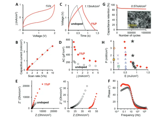
One application benefitting strongly from both the doping-induced enhanced conductivity and the inherent very high developed surface of 1%P-SiNWs are supercapacitors (SCs). To demonstrate the potential of the obtained materials in this application, we implemented them as electrodes in symmetri-cal SC devices (cf. Experimental section). Fig. 4 shows the electrochemical performance of these devices by using cyclic voltammetry (CV), galvanostatic charge–discharge (GCD) cycles and electrochemical impedance spectroscopy (EIS) techniques. Fig. 4A displays the CV curve at a scan rate of 1 V s−1revealing
Fig. 4 Electrochemical performance supercapacitors applying 1%P-SiNWs (red line/filled diamonds) compared to undoped SiNWs (black line/ empty circles). (A) CV curve at a scan rate of 1 V s−1and (B) average capacitive current density versus scan rate of 1%P-SiNWs. (C) Galvanostatic charge–discharge cycles at a current density of 1.13 mA cm−2and (D) areal capacity versus current density for both systems. (E) Nyquist plot with a magnified region at high frequency, and (F) Bode plot. (G) Cycling stability over 106GCD cycles at a current density of 0.57 mA cm−2. The inset shows a SEM image of 1%P-SiNWs after the cycling test. (H) Ragone plot (P vs. E) of 1%P-SiNW-supercapacitors of this work (red diamonds) com-pared to other state-of-the-art SiNW-based SCs: stars,37triangles,63crosses,64empty diamonds,65filled squares,18and empty squares.66
a rectangular shape without any redox peak, which denotes an excellent electrochemical double layer capacitive behavior. This tendency is constant at all scan rates from 10 to 0.01 V s−1 (Fig. S9†). The average capacitive current grows linearly with the scan rate (Fig. 4B) resulting in an areal capacity (AC) of 0.25 mF cm−2. A slight distortion of the rectangular shape CV curve was attributed to the presence of the amorphous Si layer (SiOx) (cf. Table 1 and S1†), which was found in good
agreement with the reported behavior of SiNW-based super-capacitors.66 Nevertheless, the major energy storage mecha-nism is electrochemical double layer capacitance, i.e. adsorp-tion/desorption of ions during charge/discharge. Accordingly, both 1%P- and undoped SiNWs exhibited symmetric and linear GCD profiles (Fig. 4C) with a similar small distortion. The areal capacitances derived from GCD profiles at current densities 0.1 to 5 mA cm−2 (Fig. S10†) confirm the high AC obtained by CV for 1%P-SiNWs, with 0.23 mF cm−2at 4.5 mA cm−2 (Fig. 4D). We note that 1%P-SiNWs show 2 to 4 times higher AC than undoped SiNWs, despite their 4 times lower specific area. As the capacity of an ideal conductive material is proportional to its specific area,21,65a 4 times lower AC could be expected for doped SiNWs. The observed high gain in capacity is therefore attributed to their strongly enhanced conductivity, reducing ohmic losses in the thick SiNW electrode.
Accordingly, doped SiNWs exhibited AC values ranging from 740 to 245 µF cm−2, whereas undoped SiNWs displayed AC values ranging from 255 to 120 µF cm−2 (Fig. 4D). AC shows an important initial decay reaching a plateau from 2.2 mA cm−2 with an AC value of 0.25 mF cm−2 for 1% P-SiNWs, in excellent agreement with the CV data (Fig. 4B). The EIS technique is a powerful tool to evaluate the electrode– electrolyte interface of a SC device. The Nyquist plot (Fig. 4E) shows two regions at high and low frequencies. At high fre-quencies, the semi-circle associated with the charge transfer resistance (Rct) is smaller for 1%P-SiNWs, as expected from
their higher conductivity. In this direction, at low frequencies, 1%P-SiNWs showed a more vertical line than undoped SiNWs, indicating better capacitive behavior. Besides, the impedance phase angle of doped SiNWs reached a value of approximately 70° at low frequencies (Fig. 4F), closer to the value of an ideal capacitor (90°) than undoped SiNWs (60°).
Long-term stability, another critical factor in SCs, was tested for 1%P-SiNWs (Fig. 4G) at a current density of 0.57 mA cm−2. The capacitance decayed by ∼10% in the first 10 000 cycles owing to the chemical reactions of the native silicon oxide layer and the possible presence of impurities in the elec-trolyte as previously demonstrated for CVD-grown doped SiNW64 and Si-nanotree37 based SCs. During further cycling the surface reached passivation and the capacitance was stable at >80% of its initial value for (at least) one million cycles, an excellent stability performance according to the lifetime cri-teria for supercapacitors.67 In addition, no structural degra-dation of the SiNWs after the cycling test was observed accord-ing to the SEM image depicted in the inset of Fig. 4G. The Ragone plot in Fig. 4H shows energy density values of 0.47
and 1.44 mJ cm−2at power densities of 3.9 and 2.8 mW cm−2, respectively. These values are higher than those reported in the literature for SC applying doped SiNWs obtained by other methods on a much smaller scale (e.g. CVD) and come close to the performance of the best reported system (CVD grown, doped Si nanotrees).18,37,63–66
Conclusion
This work provides a novel chemical synthesis method for pre-paring SiNWs of a small diameter (<50 nm) and controlled doping level with phosphorus (up to 1%). The use of a sacrifi-cial high-surface-area substrate (NaCl microcrystals) in combi-nation with elevated precursor loading results in a high-yield process (1 mg SiNWs per cm3 reactor volume), which can be easily scaled up as demonstrated by the use of a 150 mL reactor. Applying complementary characterization techniques, we show that successful n-type doping of the crystalline SiNW core is achieved. Phosphorus doping leads also to an unex-pected increase of the SiNW diameter. Both effects have a synergistic impact on electrical conductivity, which sharply switches from mainly resistive at a low doping level to conduc-tive at a doping level above 0.4%P. Symmetric supercapacitors based on electrodes fabricated with 1%P-SiNWs show a high areal capacity of 0.24 mF cm−2 combined with an excellent cycling stability (>1 million cycles), placing them at the top of the state of the art in the field of SiNW-based SCs. This per-formance is particularly significant considering that the present SC electrodes, made from a SiNW slurry deposited on a standard Cu current collector, lack electrical connection of the individual SiNWs. The latter is ensured in reported SCs using CVD-grown SiNWs, which have an epitaxial contact to the Si collector. To take full advantage of the good conductivity of this nanomaterial, improvements of the electrical connec-tion between individual nanowires are required to reduce ohmic losses in macroscopic SiNW assemblies. This can be achieved by modifying the outer shell of the SiNWs. We expect that the presented approach opens the way for the use of SiNWs in a wide range of electrochemical storage devices such as SCs and lithium-ion batteries, as well as in energy conver-sion devices such as thermoelectric generators.
Con
flicts of interest
There is no conflict of interest.
Acknowledgements
OB, PC and PR thank the DSM Energie program of CEA for funding. This work has been performed with the use of the Hybrid-En facility at CEA-Grenoble (France). The authors thank Thibaut Gutel in BET measurements, Eric Robin in STEM-EDX analysis, Julien Pérard in ICP-AES analysis and Stéphanie Pouget in X-ray diffraction for their help.
References
1 N. Fukata, T. Subramani, W. Jevasuwan, M. Dutta and Y. Bando, Small, 2017, 13, 1701713.
2 C. Battaglia, A. Cuevas and S. D. Wolf, Energy Environ. Sci., 2016, 9, 1552–1576.
3 B. Zhang, J. Jie, X. Zhang and X. Ou, ACS Appl. Mater. Interfaces, 2017, 9, 34527–34543.
4 X. Zuo, J. Zhu, P. Müller-Buschbaum and Y.-J. Cheng, Nano Energy, 2017, 31, 113–143.
5 B. A. Boukamp, G. C. Lesh and R. A. Huggins, J. Electrochem. Soc., 1981, 128, 725–729.
6 M. Ashuri, Q. He and L. L. Shaw, Nanoscale, 2016, 8, 74– 103.
7 C. K. Chan, H. Peng, G. Liu, K. McIlwrath, X. F. Zhang, R. A. Huggins and Y. Cui, Nat. Nanotechnol., 2008, 3, 31–35.
8 K.-Q. Peng, X. Wang, L. Li, Y. Hu and S.-T. Lee, Nano Today, 2013, 8, 75–97.
9 A. I. Hochbaum, R. Chen, R. D. Delgado, W. Liang, E. C. Garnett, M. Najarian, A. Majumdar and P. Yang, Nature, 2008, 451, 163–167.
10 V. Schmidt, J. V. Wittemann, S. Senz and U. Gösele, Adv. Mater., 2009, 21, 2681–2702.
11 A. M. Morales and C. M. Lieber, Science, 1998, 279, 208– 211.
12 Y. Cui, Z. Zhong, D. Wang, W. U. Wang and C. M. Lieber, Nano Lett., 2003, 3, 149–152.
13 P. Serre, M. Mongillo, P. Periwal, T. Baron and C. Ternon, Nanotechnology, 2015, 26, 015201.
14 J. Lee, J. Jang, B. Choi, J. Yoon, J. Y. Kim, Y. K. Choi, D. M. Kim, D. H. Kim and S. J. Choi, Sci. Rep., 2015, 5, 12286.
15 J. D. Christesen, X. Zhang, C. W. Pinion, T. A. Celano, C. J. Flynn and J. F. Cahoon, Nano Lett., 2012, 12, 6024– 6029.
16 H. Park, Y. Dan, K. Seo, Y. J. Yu, P. K. Duane, M. Wober and K. B. Crozier, Nano Lett., 2014, 14, 1804–1809.
17 Y. J. Hwang, A. Boukai and P. Yang, Nano Lett., 2009, 9, 410–415.
18 F. Thissandier, N. Pauc, T. Brousse, P. Gentile and S. Sadki, Nanoscale Res. Lett., 2013, 8, 1–5.
19 B. R. Long, M. K. Y. Chan, J. P. Greeley and A. A. Gewirth, J. Phys. Chem. C, 2011, 115, 18916–18921.
20 M. R. Zamfir, H. T. Nguyen, E. Moyen, Y. H. Lee and D. Pribat, J. Mater. Chem. A, 2013, 1, 9566–9586.
21 F. Thissandier, P. Gentile, N. Pauc, T. Brousse, G. Bidan and S. Sadki, Nano Energy, 2014, 5, 20–27.
22 V. Schmidt, J. V. Wittemann and U. Gösele, Chem. Rev., 2010, 110, 361–388.
23 S. A. Dayeh, R. Chen, Y. G. Ro and J. Sim, Mater. Sci. Semicond. Process., 2017, 62, 135–155.
24 Y. Hu, K. Q. Peng, L. Liu, Z. Qiao, X. Huang, X. L. Wu, X. M. Meng and S. T. Lee, Sci. Rep., 2014, 4, 3667.
25 K. Peng, Y. Xu, Y. Wu, Y. Yan, S.-T. Lee and J. Zhu, Small, 2005, 1, 1062–1067.
26 B. M. Bang, H. Kim, H.-K. Song, J. Cho and S. Park, Energy Environ. Sci., 2011, 4, 5013–5019.
27 B.-S. Kim, T.-W. Koo, J.-H. Lee, D. S. Kim, Y. C. Jung, S. W. Hwang, B. L. Choi, E. K. Lee, J. M. Kim and D. Whang, Nano Lett., 2009, 9, 864–869.
28 G. Flynn, K. Stokes and K. M. Ryan, Chem. Commun., 2018, 54, 5728.
29 A. T. Heitsch, D. D. Fanfair, H.-Y. Tuan and B. A. Korgel, J. Am. Chem. Soc., 2008, 130, 5436.
30 J. D. Holmes, K. P. Johnston, R. C. Doty and B. A. Korgel, Science, 2000, 287, 1471–1473.
31 H. J. Yang, F. W. Yuan and H. Y. Tuan, Chem. Commun., 2010, 46, 6105–6107.
32 H.-Y. Tuan and B. A. Korgel, Chem. Mater., 2008, 20, 1239– 1241.
33 D. C. Lee, T. Hanrath and B. A. Korgel, Angew. Chem., Int. Ed., 2005, 44, 3573–3577.
34 M. Brust, M. Walker, D. Bethell, D. J. Schiffrin and R. Whyman, J. Chem. Soc., Chem. Commun., 1994, 801–802. 35 M. J. Hostetler, J. E. Wingate, C.-J. Zhong, J. E. Harris,
R. W. Vachet, M. R. Clark, J. D. Londono, S. J. Green, J. J. Stokes, G. D. Wignall, G. L. Glish, M. D. Porter, N. D. Evans and R. W. Murray, Langmuir, 1998, 14, 17–30. 36 T. Le, P. Gentile, G. Bidan and D. Aradilla, Electrochim.
Acta, 2017, 254, 368–474.
37 D. Gaboriau, D. Aradilla, M. Brachet, J. L. Bideau, T. Brousse, G. Bidan, P. Gentile and S. Sadki, RSC Adv., 2016, 6, 81017–81027.
38 H. Geaney, E. Mullane and K. M. Ryan, J. Mater. Chem. C, 2013, 1, 4996.
39 A. T. Heitsch, V. A. Akhavan and B. A. Korgel, Chem. Mater., 2011, 23, 2697–2699.
40 J. C. Chan, H. Tran, J. W. Pattison and S. B. Rananavare, Solid-State Electron., 2010, 54, 1185–1191.
41 World Intellectual Property Organization, WO2015189827A1, 2015.
42 H. Gilman and D. H. Miles, J. Org. Chem., 1958, 23, 326– 328.
43 Y. Cui and C. M. Lieber, Science, 2001, 291, 851–853. 44 P. Schwerdtfeger, H. L. Hermann and H. Schmidbaur,
Inorg. Chem., 2003, 42, 1334–1342.
45 D. E. Perea, E. R. Hemesath, E. J. Schwalbach, J. L. Lensch-Falk, P. W. Voorhees and L. J. Lauhon, Nat. Nanotechnol., 2009, 4, 315–319.
46 C. Celle, C. Mouchet, E. Rouviere, J. P. Simonato, D. Mariolle, N. Chevalier and A. Brioude, J. Phys. Chem. C, 2010, 114, 760–765.
47 S. Piscanec, M. Cantoro, A. Ferrari, J. Zapien, Y. Lifshitz, S. Lee, S. Hofmann and J. Robertson, Phys. Rev. B: Condens. Matter Mater. Phys., 2003, 68, 241312.
48 C.-Y. Meng, J.-L. Chen, S.-C. Lee and C.-T. Chia, Phys. Rev. B: Condens. Matter Mater. Phys., 2006, 73, 245309.
49 C. K. Chan, R. N. Patel, M. J. O’Connell, B. A. Korgel and Y. Cui, ACS Nano, 2010, 4, 1443–1450.
50 T. D. Bogart, X. Lu and B. A. Korgel, Dalton Trans., 2013, 42, 12675–12680.
51 D. J. Rowe, J. S. Jeong, K. A. Mkhoyan and U. R. Kortshagen, Nano Lett., 2013, 13, 1317–1322.
52 N. Fukata, S. Matsushita, T. Tsurui, J. Chen, T. Sekiguchi, N. Uchida and K. Murakami, Phys. B, 2007, 401–402, 523– 526.
53 N. Fukata, M. Seoka, N. Saito, K. Sato, J. Chen, T. Sekiguchi and K. Murakami, Phys. B, 2009, 404, 5200– 5202.
54 D. Nobili, A. Armigliato, M. Finnetti and S. Solmi, J. Appl. Phys., 1982, 53, 1484–1491.
55 J. Safarian and M. Tangstad, J. Mater. Res., 2011, 26, 1494– 1503.
56 Reference collection NIST.
57 H. E. O’Neal, M. A. Ring, D. Kim and K. D. King, J. Phys. Chem., 1995, 99, 9397–9402.
58 P. Gentile, A. Solanki, N. Pauc, F. Oehler, B. Salem, G. Rosaz, T. Baron, M. Den Hertog and V. Calvo, Nanotechnology, 2012, 23, 215702.
59 H. Schmid, M. T. Björk, J. Knoch, S. Karg, H. Riel and W. Riess, Nano Lett., 2009, 9, 173–177.
60 A. R. Stegner, R. N. Pereira, K. Klein, R. Lechner, R. Dietmueller, M. S. Brandt, M. Stutzmann and H. Wiggers, Phys. Rev. Lett., 2008, 100, 026803.
61 Y.-C. Lin, K.-C. Lu, W.-W. Wu, J. Bai, L. J. Chen, K. N. Tu and Y. Huang, Nano Lett., 2008, 8, 913–918.
62 Y. M. Niquet, C. Delerue, D. Rideau and B. Videau, IEEE Trans. Electron Devices, 2012, 59, 1480–1487.
63 D. Aradilla, S. Sadki and G. Bidan, Synth. Met., 2019, 247, 131–143.
64 D. Aradilla, P. Gentile, G. Bidan, V. Ruiz, P. Gómez-Romero, T. J. S. Schubert, H. Sahin, E. Frackowiakf and S. Sadki, Nano Energy, 2014, 9, 273–281.
65 F. Thissandier, L. Dupré, P. Gentile, T. Brousse, G. Bidan, D. Buttard and S. Sadki, Electrochim. Acta, 2014, 117, 159– 163.
66 N. Berton, M. Brachet, F. Thissandier, J. Le Bideau, P. Gentile, G. Bidan, T. Brousse and S. Sadki, Electrochem. Commun., 2014, 41, 31–34.
67 D. Weingarth, A. Foelske-Schmitz and R. Kötz, J. Power Sources, 2013, 225, 84–88.