HAL Id: hal-01736074
https://hal.archives-ouvertes.fr/hal-01736074
Submitted on 23 Mar 2018
HAL is a multi-disciplinary open access
archive for the deposit and dissemination of
sci-entific research documents, whether they are
pub-lished or not. The documents may come from
teaching and research institutions in France or
abroad, or from public or private research centers.
L’archive ouverte pluridisciplinaire HAL, est
destinée au dépôt et à la diffusion de documents
scientifiques de niveau recherche, publiés ou non,
émanant des établissements d’enseignement et de
recherche français ou étrangers, des laboratoires
publics ou privés.
Oxidation of Si nanocrystals fabricated by
ultralow-energy ion implantation in thin SiO2 layers
H. Coffin, Caroline Bonafos, Sylvie Schamm-Chardon, Nikolay Cherkashin,
Gérard Benassayag, Alain Claverie, Marc Respaud, P. Dimitrakis, P. Normand
To cite this version:
H. Coffin, Caroline Bonafos, Sylvie Schamm-Chardon, Nikolay Cherkashin, Gérard Benassayag, et al..
Oxidation of Si nanocrystals fabricated by ultralow-energy ion implantation in thin SiO2 layers .
Jour-nal of Applied Physics, American Institute of Physics, 2006, 99 (4), pp.044302. �10.1063/1.2171785�.
�hal-01736074�
Oxidation of Si nanocrystals fabricated by ultralow-energy ion implantation in thin
layers
H. Coffin, C. Bonafos, S. Schamm, N. Cherkashin, G. Ben Assayag, A. Claverie, M. Respaud, P. Dimitrakis, and P. Normand
Citation: Journal of Applied Physics 99, 044302 (2006); doi: 10.1063/1.2171785 View online: https://doi.org/10.1063/1.2171785
View Table of Contents: http://aip.scitation.org/toc/jap/99/4 Published by the American Institute of Physics
Articles you may be interested in
Modeling stress retarded self-limiting oxidation of suspended silicon nanowires for the development of silicon nanowire-based nanodevices
Journal of Applied Physics 110, 033524 (2011); 10.1063/1.3611420 General Relationship for the Thermal Oxidation of Silicon
Journal of Applied Physics 36, 3770 (1965); 10.1063/1.1713945 Plastic analysis of cylinder oxidation
Applied Physics Letters 54, 1815 (1989); 10.1063/1.101248 Thermal oxidation of silicon nanocrystals in and NO ambient Journal of Applied Physics 93, 5637 (2003); 10.1063/1.1565172 Oxidation property of silicon small particles
Applied Physics Letters 58, 1662 (1991); 10.1063/1.105129 Self-limiting oxidation for fabricating sub-5 nm silicon nanowires Applied Physics Letters 64, 1383 (1994); 10.1063/1.111914
Oxidation of Si nanocrystals fabricated by ultralow-energy ion implantation
in thin SiO
2layers
H. Coffin, C. Bonafos,a兲S. Schamm, N. Cherkashin,b兲 G. Ben Assayag, and A. Claverie
CEMES-CNRS, 29 rue J. Marvig, 31055 Toulouse, France
M. Respaud
LNMO, INSA, Département de Physique, 135 Avenue de Rangueil, 31077 Toulouse, France
P. Dimitrakis and P. Normand
Institute of Microelectronics, NCSR “Demokritos,” 15310 Aghia Praskevi, Greece
共Received 29 July 2005; accepted 10 January 2006; published online 16 February 2006兲
The effect of thermal treatments in nitrogen-diluted oxygen on the structural characteristics of two-dimensional arrays of Si nanocrystals共NCs兲 fabricated by ultralow-energy ion implantation 共1 keV兲 in thin silicon dioxide layers is reported. The NC characteristics 共size, density, and coverage兲 have been measured by spatially resolved electron-energy-loss spectroscopy by using the spectrum-imaging mode of a scanning transmission electron microscope. Their evolution has been studied as a function of thermal treatment duration at a temperature 共900 °C兲 below the SiO2
viscoelastic point. An extended spherical Deal-Grove关J. Appl. Phys. 36, 3770 共1965兲兴 model for self-limiting oxidation of embedded silicon NCs has been carried out. It proposes that the stress effects, due to oxide deformation, slow down the NC oxidation rate and lead to a self-limiting oxide growth. The model predictions show a good agreement with the experimental results. Soft oxidation appears to be a powerful way for manipulating the NC size distribution and surface density. © 2006
American Institute of Physics.关DOI:10.1063/1.2171785兴
I. INTRODUCTION
A nanocrystal 共NC兲 memory cell consists of a metal-oxide-semiconductor field-effect transistor 共MOSFET兲 with monodisperse nanometer-scale crystals embedded within the gate dielectric.1By associating the finite-size effects of NCs and the benefits 共robustness and fault tolerance兲 of a stored charge distribution, NC memories offer an attractive alterna-tive for extending the scaling of conventional floating-gate memories 共e.g., flash nonvolatile memories兲. Various NC materials and NC self-assembling techniques have been ex-plored in the last few years. A substantial amount of investi-gation has gone into Si, Ge, or SiGe materials using different deposition techniques,1,2 thermal oxidation of Si1−xGex,
3
or ion implantation followed by annealing.4,5The possibility of fabricating Si NCs in thin SiO2 films by ultralow-energy Si implantation and subsequent thermal treatment has been re-cently demonstrated.6,7 This fabrication route is very attrac-tive because of its ability to control the size and location of a narrow NC band and its compatibility with standard comple-mentary metal-oxide semiconductor 共CMOS兲 processes. In practice, high-dose 共typically 1016cm−2兲 Si implantation in
the 1 keV range into very thin 共⬍10 nm兲 oxide layers fol-lowed by annealing at temperatures in the 900–1000 °C range allows for the formation of two-dimensional共2D兲 ar-rays of Si NCs at tunable tunneling distances from the SiO2/ Si interface.6As shown in Ref. 7, it is possible to
ac-curately control the position of the NC band by changing the
implantation and annealing conditions. In addition, Si-NC gate stacks with improved electrical performance have been obtained recently by carrying out the annealing step under slight oxidizing conditions.8Such conditions restore signifi-cantly the integrity of the oxide and lead to gate stacks suit-able for nonvolatile memory devices operating at low voltages.9Annealing in oxidizing conditions affects also the NC population.10As a consequence the oxidation step can be used for monitoring the size, density, and surface fraction of the NC population and thus for controlling the memory per-formance of the final devices. It is expected that below the viscoelastic temperature of SiO2 共950 °C兲,11,12the oxidation
of nonplanar Si structures is retarded due to normal stress induced at the Si/ SiO2 interface,13–16 thus leading to self-limiting size effects. The aim of this work is to study and model the thermal oxidation of Si NCs embedded in SiO2. NC oxidation is examined as a function of the duration of thermal treatments performed at 900 °C in nitrogen-diluted-oxygen ambient 共N2+ 1.5% O2兲. The NC characteristics 共size and aerial density兲 have been extracted from filtered images obtained by using the spectrum-imaging mode of a scanning transmission electron microscope 共STEM兲. The swelling of the SiO2 layer due to NC oxidation has been measured on cross-sectional transmission electron micros-copy共TEM兲 images. In addition, we have extended the one-dimensional 共1D兲 Deal and Grove model17 to spherical ge-ometry in order to properly model the Si NC evolution under oxidation. This model assumes that stress effects associated with nonuniform deformation of the oxide by viscous flow reduce the oxidation rate. Based on the work of Kao et
al.13,14and Omachi et al.,16it predicts the retardation of ox-ide growth on a curved surface. This retardation effect
in-a兲Author to whom correspondence should be addressed; electronic mail: bonafos@cemes.fr
b兲On leave from Ioffe Physico-Technical Institute, St. Petersburg 194021, Russia.
JOURNAL OF APPLIED PHYSICS 99, 044302共2006兲
creases when the NC size decreases, leading to a self-limiting oxide growth. The model predictions show a good agreement with the experimental results.
II. EXPERIMENTAL DETAILS AND METHODS
Silicon dioxide layers of 7 nm in thickness were ther-mally grown by dry oxidation on 8-in., p-type, 共100兲-oriented Si wafers, and subsequently implanted with 1 keV
28
Si ions to a dose of 1016Si+cm−2 using an AXCELIS GDS-ULTRA implanter. Then, the implanted samples were cleaned using a piranha solution, annealed for 30 min at 1050 °C under N2 for the purpose of NC formation, and
thermal oxidized under N2+ 1.5% O2at 900 °C for different
times 共from 5 to 240 min兲. Cross-sectional and plan-view TEM specimens were prepared by the standard procedures of grinding, dimpling, and Ar+-ion-beam thinning. Due to the
small difference in atomic number and density between Si and SiO2, the NCs show a weak amplitude and phase con-trast by TEM. Size distribution can be measured on high-resolution electron microscopy共HREM兲 images or by using dark-field conditions, but as these images are orientation de-pendent, the direct measurement of the NC surface density is impossible. Therefore, the Si NCs were imaged on a plan-view specimen by performing parallel electron-energy-loss spectroscopy 共PEELS兲 in a scanning transmission electron microscope, VG-HB 501 operating at 100 kV, using the spectrum-image technique 共called PEELS-STEM in the following兲.18
This microscope is equipped with a field-emission cathode and a parallel Gatan 666 EELS spectrom-eter. The EELS spectra were recorded over the first 50 eV on each image point of the specimen共typically 256⫻256兲. The EELS experiment is performed in the low-energy-loss do-main. Plasmons, corresponding to plasma oscillations of va-lence electrons associated with each phase of the analyzed area, are the major signatures in this energy domain of the EELS spectra. Bulk silicon and silica plasmons are located at 17 and 23.5 eV, respectively. They are well separated and thus can be used to get the image associated with the corre-sponding phase. After acquisition of a spectrum at each point of the image, contributions from silicon plasmon and silica plasmon are isolated by reconstruction of the signal with reference spectra of Si and silica. Then a map can be dis-played where the gray levels are defined by the weight of Si deduced from the reconstruction parameters. On such “chemical images,” all the Si NCs are visible, amorphous, eith crystalline, and in the last case whatever their orientation is. A contrast enhancement method is applied to these images in order to perform quantitative measurements such as the NC mean size and aerial density and surface fraction and number of atoms stored within the NCs. In order to control the homogeneity of the NC distribution throughout the plan-view TEM samples, energy filtering transmission electron microscopy共EFTEM兲 experiments have also been performed for particular samples. By inserting an energy-selecting slit in the energy-dispersive plane of the filter at the Si plasmon energy, the population of Si NCs can also be visualized. A TEM-FEG microscope, Tecnai F20ST equipped with an en-ergy filter, TRIDIEM from Gatan was used. The contrast in
the EFTEM raw images is less than in the PEELS-STEM technique because there is a contribution of the silica plas-mon signal at the plasplas-mon energy of Si. However, after ap-plying the contrast enhancement method, the two types of images became comparable.
Cross-sectional TEM共XTEM兲 studies were carried out using a CM30 Philips TEM equipped with a LaB6 cathode
operating at 300 kV and having a nominal resolution of 0.19 nm. These observations aim at measuring the depth position of the NC layer in the SiO2 layer and, in particular, the
location of the NCs in respect to the Si substrate and the surface. For this, we have developed a method for fast and accurate distance measurements using Fresnel contrast.19As mentioned earlier, the difference between the mean atomic numbers and the densities in Si and SiO2are small so the Si
NCs show no amplitude contrast when buried in a SiO2
layer. Nevertheless, the electrostatic potentials being slightly different in Si and SiO2, some small phase shift exists be-tween electron waves having propagated or not through the NC layer. This phase shift can be “imaged” by using strongly defocused bright-field conditions, provided the incident beam is highly coherent. Under such conditions, a pair of 共black/white or white/black兲 Fresnel fringes appears exactly centered on each interface. Microdensitometric analysis of such images can be performed using an online charge-coupled device 共CCD兲 camera and image processing facili-ties so that averaging of the gray levels along the direction perpendicular to the layers can be represented by a “line scan.” Thus, on such experimental densitometric profiles, all the distances of interest can be precisely measured by locat-ing the inflexion points of each pair of black and white fringes originating from the different interfaces. The uncer-tainty of these distance measurements is estimated to be ±0.5 nm. Finally, a poly-Si layer has been deposited after annealing on top of the samples in order to facilitate the distance measurement with respect to the surface.
III. EXPERIMENTAL RESULTS
As shown in Ref. 20 the NC characteristics strongly de-pend on the implanted dose. When implanting at 1 keV no NCs are detected for doses below 5⫻1015cm−2, while a
high dense array of spherelike NCs is formed at a medium dose 共1016 cm−2兲 and a connected array of elongated NCs
with a larger size and less density is formed at a highest dose 共2⫻1016cm−2兲. In the last case, annealing under N
2+ O2has
been shown to be an efficient way for separating the con-nected NCs.21 In this work, we have chosen to study the oxidation process of Si NCs embedded in SiO2in the case of
the medium range fluence共1016cm−2兲 for which a high
den-sity of well-separated spherical NCs is observed after anneal-ing at 1050 °C for 30 min under N2关see Fig. 1共a兲兴. After this
high-temperature NC formation step, the NCs were oxidized at 900 °C for different durations 共between 5 and 240 min兲. As reported above, the oxidation temperature being above the viscoelastic temperature关950 °C for thermal SiO2共Refs.
11 and 12兲兴, a self-limiting oxidation process is expected.22,23
As it appears in the PEELS-STEM images of Fig. 1 and on the graph shown in Fig. 2共a兲, the average size of the NCs
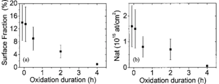
共square symbols兲 slowly decreases from 2.9±0.3 nm for the reference sample共N2, 1050 °C, 30 min兲 to 1.8±0.2 nm for a sample annealed under N2+ O2during 240 min. Meanwhile,
the NC density 关see Fig. 2共b兲兴 decreases by a factor of 10. Thus, the surface fraction 共coverage兲 decreases from 12% after 5 min to 1% after 240 min of annealing关see Fig. 3共a兲兴. This corresponds to a decrease of the number of Si atoms by a surface unit contained within the NCs from 1.4⫻1015 to
1014at. cm2 关see Fig. 3共b兲兴, indicating that the progressive
oxidation of the nanoclusters takes place. As we can see in Figs. 2 and 3, this evolution takes place following two stages. During the first 60 min the size and NC density lin-early decrease and then, for longer annealing times, the con-sumption of silicon slows down and stabilizes.
XTEM observations共see Fig. 4兲 have allowed the mea-surement of the different characteristic distances—SiO2
thickness 共eSiO
2兲, injection distance 共dinj, SiO2 thickness
be-tween the Si/ SiO2interface and the NC layer兲, width of the
NC layer 共encs兲, and gate distance 共dgate, SiO2 thickness be-tween the NC layer and the SiO2 surface兲—by using the
method described in Ref. 19. The cross-sectional scheme in Fig. 5 shows the quantitative evolution of these distances共x axis兲 for different annealing durations 共y axis兲. As we can see in Fig. 5, the width of the NC layer slightly decreases with an increase of the annealing time under N2+ O2. For
oxida-tion duraoxida-tion larger than 30 min, the contrast of the NC layer is very weak, due to the small density of particles, and the evaluation of the NC layer width is no more possible. On the other hand, the whole oxide thickness increases when in-creasing the oxidation duration 共from 10.4±0.5 initially to 13.2± 0.5 nm after 240 min兲. It is important to point out that this swelling concerns both the control and the injection ox-ide: the SiO2/ Si interface is therefore also oxidized in addi-tion to the NCs.
IV. MODELING OF THE SI NANOCRYSTAL OXIDATION
The most comprehensive characterization of the stress effects during oxidation of nonplanar Si structures was per-formed by Kao et al.13,14 These authors have extended the one-dimensional stress-free model of Deal and Grove17 to the oxidation of nonplanar silicon structures, i.e., to concave and convex cylindrical 2D structures. For this, they treated the oxide as an incompressible viscous fluid being driven by a velocity field at the silicon/oxide interface.
This assumption共SiO2is a viscous fluid兲 is, in fact, valid above the viscous flow point共950 °C兲, while at low tempera-tures 共below 800 °C兲 SiO2 behaves as an elastic solid.11,12 Between these extremes, it presents more complex mechani-cal characteristics and for modeling stress effects during non-planar oxidation, several authors have considered a vis-coelastic behavior, which mixes both reversible elastic deformation and steady flow process.24
A further improvement of the modeling of stress effects in silicon oxidation led to the introduction of shear-stress-dependent viscosity.24–26This stress effect is, in fact, similar to a plastic phenomenon and gives a nonlinear behavior to the material. Indeed, it is known from the experiment that SiO2becomes more fluidic under a high stress state,27
lead-ing to a strong modification of its viscosity. The lowered viscosity at a high stress level results in a slower increase of the oxide stress when increasing the interfacial curvature than would otherwise occur. Plasticity has been incorporated in both viscoelastic and viscous formulations.24–26,28For 2D cylinders, it has been shown that linear viscous models usu-ally overpredict the stress by two orders of magnitude at low temperature even if the viscoelastic solution approaches the plastic solution at high temperature.28In addition, still for 2D structures, the linear viscous flow models generate stress val-ues larger, especially at low temperatures, than the threshold value for plastic deformation 共for SiO2 109dyn/ cm2, i.e.,
108Pa兲.28
At last, taking into account nonlinearity deforma-tion has been proven to be crucial for the successful fitting of the experimental results for concave structures.25,26
In our experimental case 共dry oxidation at 900 °C for
FIG. 2. Evolution of共a兲 the Si NC mean radius and 共b兲 of the NC aerial density vs annealing time under N2+ O2, as measured on the images in Fig. 1. In共a兲 the model predictions for ⍀=25 Å3and⍀=12.5 Å3are plotted in the solid and dashed lines, respectively.
FIG. 3. Evolution of 共a兲 the percentage of surface occupied by Si NCs 共coverage兲 and 共b兲 of the number of silicon atoms within the NCs vs the annealing time under N2+ O2, deduced from the images in Fig. 1.
FIG. 4. XTEM images of 共a兲 reference sample 共N2兲; 关共b兲–共d兲兴 oxidized samples for 5, 30, and 240 min, respectively.
FIG. 1. Plan-view PEELS-STEM images of共a兲 reference sample 共N2兲; 关共b兲– 共d兲兴 oxidized samples after 5, 30, and 240 min, respectively. The contrast of the original images has been enhanced.
some hours兲 we have evaluated by a simple calculation the time for viscous flow to develop, that is, the time for the stress to reach the steady-state value.29This time is, by using a linear model and viscosity values measured by Fargeix and Ghibaudo,30 of about 50 min, i.e., smaller than the whole oxidation duration共some hours兲. As a consequence, we have assumed in our model a deformation of SiO2 by viscous
flow. This assumption is in agreement with EerNisse’s ex-perimental measurements11 of diagnostics viscous flow of dry and wet SiO2 when annealing at 925 °C for oxidation times larger than 20 min. In addition, we have considered that the thermal budget 共900 °C for some hours兲 was suffi-ciently high that we can neglect plastic deformation and as-sume linear deformation and a pressure-dependent viscosity, as described by Dane and Birch31 and not a shear-modulus-dependent viscosity linked to plasticity effects.24–26In other words, we treated the oxide as an incompressible viscous fluid as Kao et al.13,14 and Omachi et al.16 also did. The obtained stress levels will be discussed in Sec. V and com-pared to the threshold stress value for plastic deformation.
The 2D model of Kao et al.,13,14 which concerns the micrometric concave and convex cylindrical structures under wet oxidation, has been extended to the three-dimensional 共3D兲 spherical conditions by Chen and applied to nanocrys-talline Si quantum dots under dry oxidation.15 To avoid a tedious fluid mechanics analysis of oxide stress, these au-thors have used an approximate scale analysis and assumed the influence of stress on the diffusion and solid solubility constant to be much less important than the influence on the chemical reaction rate. Omachi et al.16 have included these effects in their model. Nevertheless, their model implies not less than five fitting parameters and a good agreement with the experiment is obtained for values of the zero-pressure
viscosity of 1012 poises, i.e., three orders of magnitude less than measured at this temperature 共850 °C兲 for dry oxidation.30
To model the oxidation process of our system, i.e., Si NCs embedded within a thin SiO2 matrix, we have used the extension of the Deal and Grove model to 3D geometry of Omachi et al.,16implying both normal stress at the interface and hydrostatic pressure in the oxide volume. A particular attention has been paid in limiting the number of fitting pa-rameters and in using realistic constants. This model predicts the evolution during annealing under oxidizing ambient of a NC with an initial size, the average radius of the NC popu-lation after the nucleation stage共reference sample兲.
Classically, the oxidation is divided into three processes which are associated with three fluxes关see Fig. 6共a兲兴.17The first flux F1concerns the diffusion of oxidizing species共O2兲
at the gas/oxide interface, the second flux F2 is associated
with the diffusion of the oxidizing species into the SiO2, and
the third flux F3 represents the flux of oxidizing species at
the Si/ SiO2interface. These three fluxes can be expressed as
F1= h共C*− C0兲, 共1兲
F2= − D
dC
dr, 共2兲
F3= ksCi, 共3兲
where h is the surface mass transfer constant of oxidant, D is the diffusivity of oxidant in the SiO2, ksis the surface
reac-tion rate constant at the SiO2/ Si interface, C*is the oxidant
solubility in SiO2, Ciis the concentration of oxidant near the
Si/ SiO2interface, and C0is the concentration of the oxidant
at the outer surface of the oxide.
In the Deal and Grove model, the three fluxes are set equal due to the steady-state condition. The steady-state dif-fusion equation inside the oxide is given by
ⵜ2C = 1 r2 r
冉
r 2C r冊
= 0. 共4兲The solution of this Laplace equation in spherical coordi-nates is a hyperbole fragment, C共r兲=A+B/r. Considering that the mass transport is conserved for any radius r and combining Eqs.共1兲–共4兲 the oxidation rate for a spherical Si NC can be expressed as15,16
FIG. 5. Cross-sectional scheme depicting the evolution of the characteristic distances as a function of the oxidation duration, from 0共reference sample兲 to 240 min at 900 °C共y axis兲. These distances were measured on the XTEM images of Fig. 4 and are plotted on the x axis. Up triangles: distance be-tween the bottom edge of the NC layer and the Si substrate共injection dis-tance兲. Down triangles: distance between the top edge of the NC layer and the Si substrate. Squares: distance between the polysilicon layer and the Si substrate共SiO2thickness兲. All the distances are measured with an accuracy of ±0.5 nm. In the inset, a XTEM image is shown where all these distances are defined.
FIG. 6. Schematics of共a兲 a spherical Si NC surrounded by an oxide shell with normal compressive stress at the interface共兲 and tensile stress 共hy-drostatic pressure, P兲 within the oxide volume, which appear during the viscous flow of the growing oxide and 共b兲 of two neighboring NCs sur-rounded by their oxide shell.
dx dt = 1 N C* 1/ks+ a2/b2h + a共b − a兲/bD . 共5兲 Instead of dx dt = 1 N C* 1/ks+ 1/h +共1/D0兲共b − a兲
for planar oxidation.17x = b − a with a is the NC core radius
and b is the radius of the NC core plus oxide shell关see Fig. 6共a兲兴, both varying with time. N is the number of oxidant molecules incorporated into SiO2 per unit volume of oxide grown. N = 2.2⫻1022molecules/ cm3 for dry oxidation by
considering that one O2 molecule is incorporated into each SiO2molecule. Because of volume conservation, the Si core radius, a, and the core + shell radius, b, are not independent variables.15 We assume an incompressible fluidic oxide and the ratio of produced SiO2 volume to the consumed Si vol-ume 2.25共=45/20兲: 1. If the starting radius of Si core is a0
and the starting radius of the core + shell sphere is b0, the above assumption results in the following relation between a and b:15
b3+ 1.25a3= b03+ 1.25a03= B. 共6兲
The evolution of the new NC radius a共t兲 is thus given by
da dt = − dx dt 1 1 + 1.25a2共B − 1.25a3兲−2/3. 共7兲 As shown by Kao et al.,13,14the oxidation of non-planar-structured Si must take into account the influence of stress at the Si/ SiO2interface. Indeed, as the volume of grown oxide is larger than the initial volume of Si, the material should expand. As a result, the newly formed oxide pushes the old one which rearranges itself through viscous flow. The struc-ture relaxes towards equilibrium according to the mechanical properties of the oxide which are characterized by fluid de-formations. Following Kao et al.,13,14two types of stress are generated that retard the oxidation process. One is the nor-mal compressive stressgenerated at the Si NC / SiO2
inter-face and the other one is the tensile stress P 共hydrostatic pressure兲 generated in the oxide shell 关see Fig. 6共a兲兴.
For 3D structures, the normal stress at the Si NC inter-face is given by15,16
= − 4
冉
1a3−
1
b3
冊
, 共8兲whereis the viscosity andis the velocity constant, which is a function of the oxide velocity at the interface. Based on the work of Omachi et al.,16we take the following sign con-vention for stress: positive for tension and negative for com-pression. The effect of this normal stress is to reduce the surface reaction rate 共ks兲 by adding to activation energy the
extra work which has to be carried out by the expanding oxide,13–16
ks= ksoexp
冉
⍀kT
冊
, 共9兲with⍀ the volume expansion and ksothe stress-free value of
ks.
For planar oxidation, ksovaries with the oxygen partial
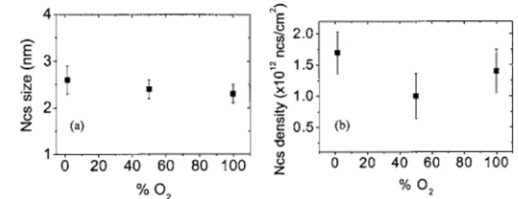
pressure.17,32,33Nevertheless, the NC population is found the same in the experimental error bars 共in average size and aerial density兲 when oxidizing under 1.5% of O2 and 100%
O2 共see Fig. 7兲. The oxidation of the particles is therefore
independent of the O2 content. As a consequence, kso has
been taken here independent of the oxygen partial pressure. The parameter⍀ has the physical significance of the reaction jump volume in the Si to SiO2 transition. The model states
here that the oxidizing species need to have enough energy to move the newly formed oxide against the normal force field
. The energy required in a unit reaction is the product of the reaction jump volume⍀ and. Initially,⍀ was taken equal to ⍀SiO2−⍀Si= 25 Å3,13–16 while Sutardja et al.25 and
Su-tardja and Oldman26argued that a unit reaction involves the breaking of one Si–Si bond and the attachment of a bridging oxygen atom between the two Si atoms. In this case,⍀ must be close to 12.5 Å3, the difference between the volume of
Si–O and Si. In our model, these two cases have been con-sidered. This normal stress makes the reaction at the silicon NC surface more difficult and affects the surface reaction rate which decreases as the normal stress compressively in-creases.
The hydrostatic pressure in the oxide volume 共P兲 is given by16
P = 41
b3. 共10兲
This stress is created in the bulk of the old oxide which is stretched and being pushed out and is tensile for convex surfaces. The diffusivity D and the solubility C* of the
oxi-dant are increased by tension while it is the opposite for the viscosity,13,14,16 D = D0exp
冉
PVa kT冊
, 共11兲 C*= C0*exp冉
PVs kT冊
, 共12兲 =0exp共−␣P兲, 共13兲where D0, C0*, and 0 are, respectively, the zero-pressure
diffusivity, solubility, and viscosity. Vaand Vsare the
activa-tion volumes of diffusivity and solubility.␣ is an empirical
FIG. 7. Evolution of共a兲 the NC mean radius and 共b兲 NC density vs the O2 content, as measured on plan-view PEELS-STEM images. The samples have been implanted at 1 keV with a dose of 2⫻106cm−2, annealed under N2during 30 min at 1050 °C and under N2-diluted O2with 1.5% O2, 50% O2, and 100% O2at 900 °C for 30 min.
parameter. We assume here the pressure-dependent oxide viscosity model proposed by Kao et al.13,14As the tensile stress increases the O2 diffusivity and solubility increase
while the viscosity decreases. Then, the oxidant transport and the viscous flow are enhanced comparing to zero-pressure conditions. The two stressesand P are functions of viscos-ity which has a strong temperature dependence. Therefore, the normal and hydrostatic stresses are both higher at low temperatures for which the viscosity is much larger and it is more difficult for the oxide to flow. By taking into account these stress effects, the oxidation rate can be written as
dx dt = C1exp共⍀/kT兲 1 + exp共⍀/kT兲兵共a2/b2兲C 2+关a共b − a兲/b兴C3其 , 共14兲 with C1= C10exp
冉
PVs kT冊
and C10= C0*kso N =冉
B A冊
DG, 共15兲 C2= C20=kso h , 共16兲 C3= C30 exp共PVa/kT兲 and C30= kso D0 = 2冉
B A冊
DG冒
BDG. 共17兲C10 and C30 are deduced from the linear and parabolic
con-stants 共B/A兲DG and BDG of the 1D Deal and Grove 共DG兲
oxidation model17 and depend only on the temperature and Si orientation. We considered here for the dots a共111兲 orien-tation even if they are, in fact, randomly oriented. Indeed, for this orientation the oxidation velocity ranges in between the velocity for共110兲 orientation, which is the fastest and the one for共100兲 orientation, which is the slowest. C20is more
prob-lematic to evaluate as depending on h, the gas-phase mass transfer coefficient, which is a function of the furnace con-figuration. Nevertheless, in our calculation, the term depend-ing on C2 is always negligible, when considering classical
values for h, taken from the literature.15,17
The time evolution of the oxidation rate is solved by means of a Runge-Kutta method. The initial values of a and
b are taken from the experiment: a0= 1.5 nm is the NC mean radius for the reference 共nonoxidized兲 sample, as measured on the images in Fig. 1. Our system differs from those pre-viously studied in the literature because the NCs are embed-ded within SiO2and not deposited on top of it. Indeed, in our case a shell of SiO2surrounds the NCs before the beginning of the oxidation process and this shell is larger than the NC radius itself. This oxide shell is anisotropic in dimension as the average distance between the NCs 共lateral distance, d兲 can be different from the distance of the precipitates to the free surface共perpendicular distance, Rp兲, see Fig. 6共b兲. The
average distance 共d兲 between the precipitates can be calcu-lated from the NC density and ranges between 4 and 6 nm following the model considered 共hexagonal-type compact stacking or a classical cubic one兲. This leads to an oxide shell
b01= d − a0 ranging from 3 to 5.5 nm关see Fig. 6共b兲兴. On the
other hand the distance of the NCs to the surface 共perpen-dicular distance兲 can be measured on XTEM images and is
b02= Rp= 4.5± 0.5 nm. This value ranges in between the two
values found for b0 when considering lateral distances.
Therefore the anisotropy of the system is not very important 共1.5±0.5 nm兲. Finally, the impact of the initial value of the oxide shell 共b0兲 on the simulation has been tested and we
have seen that a decrease of b0 leads to an increase of the
viscosity 共and inversely兲 to fit the experimental evolution. Anyway, these viscosity values always range in the expected ones at this temperature.30 We have taken in our model x0
= b0− a0 on the order of the control gate oxide thickness at
t = 0, and therefore b0= 4.5 nm 共perpendicular distance兲, as
measured in the XTEM images in Fig. 4.
Omachi et al.16used the activation volumes of solubility and diffusivity, Vsand Va, respectively, as fitting parameters.
For wet oxidation, Kao et al.13,14have shown that Vsmust be
of the same order of magnitude as the molecular volume of H2O. In this direction, we have considered Vsof the order of
magnitude of the molecular volume of O2, i.e., 20 Å3,34 for
dry oxidation. Concerning Va, a large range of values can be
found in the literature, from 75 to 600 Å3.16,24,25These val-ues are deduced by experimental data fitting. By using Vain
the 75–600 A3range, our simulation results indicate that this
parameter has no significant impact on the oxidation rate. As a consequence, the zero-pressure viscosity,0, and the pres-sure coefficient for viscosity, ␣, are the only fitting param-eters needed in our model for describing the thermal oxida-tion of NCs.
Also, by considering these input values, we obtain exp共⍀/kT兲兵共a2/ b2兲C
2+关a共b−a兲/b兴C3其Ⰶ1, i.e., 1 / ks
Ⰷa2/ b2h + a共b−a兲/bD. In other words, the oxidation process
does not depend on the diffusion coefficient and is only a function of ks, the surface reaction rate. The oxidation is
therefore reaction limited, as it is the case in planar oxidation for thin oxides.17
Under this condition, the expression of the oxidation rate can be simplified to dx dt = C10exp
冉
PVs kT冊
exp冉
⍀ kT冊
. 共18兲V. COMPARISON OF THEORY AND EXPERIMENTS
Concerning the evolution of the NC mean radius during oxidation, as mentioned in Sec. III, we observe that the size of the NCs decreases and saturates when increasing the oxi-dation time. This evidences that the oxioxi-dation rate slows down as the silicon nanocluster radius becomes smaller, i.e., that we have a self-limited oxidation process. In the case of ⍀=25 Å3, we obtain a good agreement between our model
and the experimental data关see Fig. 2共a兲 in solid line兴 for a viscosity of 0= 7⫻1014 poises and for ␣= 1.5⫻10−8Pa−1,
i.e., of the order of magnitude of the one proposed in Refs. 13 and 16. When taking⍀=12.5 Å3, the model fits with the
experimental results for a value of viscosity of 3⫻1015
poises关see Fig. 2共a兲 in dashed line兴. These values of viscos-ity are very close to the one found by Fargeix and Ghibaudo 共1.5⫻1015poises兲 for dry oxides.30
While the value taken for
␣has no strong impact on calculation, this is not the case for
the zero-pressure viscosity 共0兲 at low temperatures; the
smaller is the viscosity, the faster is the oxidation. As a con-sequence, the only parameter that affects oxidation is0. The
agreement between our experimental data and simulation for realistic values of the viscosity renders our model credible.
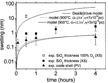
The oxide shell dimension共b−a兲 can be deduced from the experiment by subtracting the average volume of the NCs before and after each step of oxidation, calculated from the experimental mean radius and taking into account the corre-sponding volume expansion. The evolution of this shell di-mension is plotted in Fig. 8 with triangle symbols. We ob-serve a good agreement between the shell values predicted by our model 共Fig. 8, solid and dashed lines following the value of⍀兲 and the experimental values. As already empha-sized in Refs. 16, 22, 23, and 35, the oxidation of 3D NCs is slower than the one predicted by the classical Deal and Grove model for a planar interface, as plotted in the dot-dashed line in Fig. 8.17 This theoretical evolution even un-derestimates the oxidation rate which is enhanced for thin oxides共below 25 nm兲.36We can also notice that, for oxida-tion times larger than 5 min the expansion of the whole SiO2 layer 共square symbols in Fig. 8兲, deduced from Fig. 5, is much larger than these shell values共triangle symbols in Fig. 8兲. This discrepancy is due to the SiO2/ Si interface oxidation
already mentioned in Sec. III. Anyway, this interface oxida-tion is several times smaller than the one predicted by the planar oxidation Deal and Grove model 共dot-dashed line兲.17 This can be explained by the percentage of O2which is 1.5%
instead of 100%. Indeed, if there is no effect of the O2
pres-sure on the NC reaction rate because the oxidation process is mainly limited by the stress effects, this is not the case for the oxidation rate of the SiO2/ Si substrate interface. By
com-parison, the oxide swelling for the sample annealed with 100% O2 at 900 °C for 30 min 共open square in Fig. 8兲 is
10± 0.5 nm larger than the one for the 1.5% O2 at this
ther-mal budget. This expansion is even larger than the one ex-pected by the Deal and Grove theory, as predicted by Mas-soud et al.36
In Fig. 9, we have plotted the compressive normal stress
at the interface of the NCs 共in absolute value兲 and the tensile stress in the oxide bulk共hydrostatic pressure兲 P in the bulk oxide predicted by the model during oxidation. When increasing the oxidation duration, increases in absolute value, leading to a decrease of the reaction rate ksand
there-fore a retardation of the oxidation process. On the other hand, the tensile stress in the volume, P, decreases during oxidation, leading to a decrease of the O2 diffusivity and solubility, even if both of them remain larger than the values at zero pressure. In particular, the decrease of the solubility during oxidation contributes to the retardation of the oxida-tion process. The decrease of the hydrostatic pressure during oxidation also leads to an increase of the viscosity that in-creases the normal strain at the interface共in absolute value兲 and therefore contributes also to the retardation of the oxida-tion process.
A good agreement between our model and the experi-mental evolution is obtained by considering both the effect of the normal stress at the interface共兲 and the stress in the volume共P兲. When considering only one of these two stresses the model fails in describing the experimental evolution. When taking into account P only while the oxidation rate is several times faster than when taking into account both P and. Foronly, a quasilinear evolution of the NC radius is found and fails in fitting the experimental evolution, what-ever the considered viscosity and volume expansion共⍀兲.
For the considered viscosity, the values of the compres-sive stress at the interface and the tensile stress in the oxide volume are of the order of some 109and 108Pa, respectively,
and this, for the two values considered for ⍀. These stress values are of the order of magnitude of the ones obtained by Dalla Torre et al. by using Monte Carlo calculation of the oxidation of very small Si NCs.34
We carried out all the calculations in this model assum-ing Newtonian flow of the oxide but, as mentioned in Sec.
FIG. 8. Experimental evolution vs annealing time of the swelling with re-spect to the nonoxidized sample of the whole SiO2layer measured in XTEM 共plain squares for 1.5% O2and empty squares for 100% O2兲 and of the thickness increase of the SiO2shell generated by the Si NC oxidation, as deduced from plan-view measurements共up triangles兲. In the dot-dashed line is plotted the model predictions for planar oxidation共1D Deal and Grove model兲 and in the solid and dashed lines our model results for 3D oxidation 共for, respectively, ⍀=25 Å3and⍀=12.5 Å3兲.
FIG. 9. Evolution of compressive stress 共in absolute value兲 and tensile stress P vs the annealing time for⍀=25 Å3.
IV, it was observed that at high temperature the flow of glasses is nonlinear at high stresses.24–26,28The stress level is here larger than that critical stress for nonlinear behaviors 共c= 108Pa兲, suggesting that our model is limited and that
the plastic flow should be considered. Nevertheless, this critical stress value, used in the actual plastic models, is mea-sured for silica glass for which the viscosity and the glass transition temperature are different from dry thermal SiO2.37
It is therefore difficult to take this value as an absolute threshold. In addition, the stress values that we obtained are in good agreement with those measured by Raman for NC ion beam synthesized in SiO2共⬃1 GPa兲,38 and this stress level is still lower than the threshold value for the fracture of a Si wafer共10–25 GPa兲.39
A last point to clarify lies in the important decrease of the NC aerial density, which falls down from 2.2共±0.4兲 ⫻1012to 2.5共±0.5兲⫻1011cm−2, as experimentally observed
on Fig. 2共b兲. Even if the average diameter of the NCs de-creases down to 2 ± 0.2 nm, this value is still larger than the visibility threshold in the PEELS-STEM images, which lies around 1 nm. Nevertheless, the NCs are size distributed共see inset of Fig. 10 for the nonoxidized sample兲 and the simula-tion of Fig. 2共a兲 共or reported in the dot-dashed line in Fig. 10兲 concerns only the NCs having the average size of the population共1.5 nm兲. The NCs initially larger than the aver-age size, for instance, those having a radius of 2 nm, are shrinking faster as their initial oxidation velocity is higher 共see Fig. 10 in solid line兲. For this reason, after 100 min of annealing, their size is smaller than the one reached by the NCs starting with a radius of 1.5 nm.
Anyway, even if shrinking faster, they are still larger than the visibility limit at the end of the oxidation. On the other hand, around 50% of the NCs for the nonoxidized sample are smaller than the average size 共see inset of Fig. 10兲. The simulation of the oxidation of precipitates having 1 nm in diameter is also shown in Fig. 10共dashed line兲. After 240 min of annealing, this class of NCs has an average
di-ameter of around 1.2 nm, i.e., close to the visibility limit. We can consider therefore that 50% of the NCs have disappeared during the oxidation annealing. This dissolution does not ex-plain the decrease of 90% in density observed in Fig. 2共b兲 but one has to take into account that during annealing the NCs naturally encompass a competitive growth called Ost-wald ripening40where the NC density naturally decreases. A study of the evolution of the NC population, when annealing in this range of temperature under N2 only, shows a natural
decrease of the NC density of 40% while the mean radius only slightly increases, due to a nonconservative ripening process. The important decrease of the density as observed in Fig. 2共a兲 can be therefore attributed to the cumulative effect of these two processes.
VI. CONCLUSION
In conclusion, thermal treatments in N2-diluted O2 at a temperature below the viscoelastic temperature of SiO2 共950 °C兲 appear to be a powerful way for manipulating the size distribution and surface density of 2D arrays of NCs embedded in thin SiO2films. Our experiments performed at 900 °C in 1.5% O2reveal that the NC mean size, density, and
surface fraction significantly decrease with annealing dura-tion, while the oxidation rate of the NCs slows down with time and stabilizes after 1 h annealing, thus indicating a self-limiting oxidation process. The Si substrate/SiO2interface is
also oxidized but at a rate slower than the one predicted for planar oxidation. This discrepancy is due to the limited O2
content used in our experiments. The effect of thermal oxi-dation on the Si NC size can be predicted by means of an extended spherical Deal-Grove model taking into account a stress-induced retardation process. The oxidation process is reaction limited and both共a兲 normal stress at the Si NC in-terface that retards the reaction rate constant ks and共b兲
ten-sile stress in the bulk oxide that modifies the oxide viscosity and oxygen solubility in the oxide must be considered. The reaction rate being strongly limited by these stress effects, the O2 percentage has no effect on the NC oxidation itself.
The stress values required in our 3D model are smaller than the threshold for Si wafer fracture, but high enough for sug-gesting that possible effects of plasticity occur during SiO2 deformation. This last phenomenon is under investigation and will be discussed in detail later together with the thermal oxidation of NCs at temperatures above the viscoelastic point. Finally, the electrical properties of the NC gate stacks herein reported have been studied and will be published in the close future.
ACKNOWLEDGMENTS
The authors would like to thank V. Soncini from ST Microelectronics Agrate for the oxidized wafers, A. Agarwal from Axcelis Technologies Inc. for the implantations, and M. Tencé and C. Colliex from LPS Orsay for PEELS-STEM images. The authors also gratefully acknowledge C. Krzem-inski from IEMN Lille for fruitful discussions on the kinetics of oxidation.
FIG. 10. Simulation of the evolution of the NC mean radius during oxida-tion for the different classes of size共a0= 1 nm, a0= 1.5 nm, and a0= 2 nm兲 encountered in the initial size histogram, shown in the inset, of the reference sample 共nonoxidized兲. The simulations have been carried out with ⍀ = 12.5 Å3and
0= 1.5⫻1015poises.
1S. Tiwari, F. Rana, H. I. Hanafi, A. Hartstein, E. F. Crabbé, and K. Chan, Appl. Phys. Lett. 68, 1377共1996兲.
2G. Ammendola et al., J. Vac. Sci. Technol. B 20, 2075共2002兲. 3Y. C. King, T. J. King, and C. Hu, IEEE Trans. Electron Devices ED-48,
696共2001兲.
4H. I. Hanafi, S. Tiwari, and I. Khan, IEEE Trans. Electron Devices 43, 1553共1996兲.
5P. Normand, D. Tsoukalas, E. Kapetanakis, J. van den Berg, D. G. Ar-mour, J. Stoemenos, and C. Vieu, Electrochem. Solid-State Lett. 1, 88 共1998兲.
6P. Normand et al., Nucl. Instrum. Methods Phys. Res. B 178, 74共2001兲. 7C. Bonafos, M. Carrada, N. Cherkashin, H. Coffin, D. Chassaing, G. Ben
Assayag, and A. Claverie, J. Appl. Phys. 95, 5696共2004兲. 8P. Normand et al., Appl. Phys. Lett. 83, 168共2003兲. 9P. Dimitrakis et al., Solid-State Electron. 48, 1511共2004兲. 10H. Coffin et al., Mater. Res. Soc. Symp. Proc. 830, D6.6共2005兲. 11E. P. EerNisse, Appl. Phys. Lett. 30, 290共1977兲.
12E. P. EerNisse, Appl. Phys. Lett. 35, 8共1979兲.
13D. B. Kao, J. P. McVittie, W. D. Nix, and K. C. Saraswat, IEEE Trans. Electron Devices ED-35, 25共1988兲.
14D. B. Kao, J. P. McVittie, W. D. Nix, and K. C. Saraswat, Tech. Dig. - Int. Electron Devices Meet. 1985, 388.
15Y. Chen, Microelectron. Eng. 57–58, 897共2001兲.
16J. Omachi, R. Nakamura, K. Nishiguchi, and S. Oda, Mater. Res. Soc. Symp. Proc. 638, F531共2001兲.
17B. E. Deal and A. S. Grove, J. Appl. Phys. 36, 3770共1965兲. 18C. Jeanguillaume and C. Colliex, Ultramicroscopy 28, 252共1989兲. 19G. B. Assayag, C. Bonafos, M. Carrada, A. Claverie, P. Normand, and D.
Tsoukalas, Appl. Phys. Lett. 82, 200共2003兲. 20T. Müller et al., Appl. Phys. Lett. 85, 2373共2004兲.
21C. Bonafos et al., Mater. Res. Soc. Symp. Proc. 830, D5.2共2005兲. 22H. I. Liu, D. K. Biegelsen, N. M. Johnson, F. A. Ponce, and R. F. W.
Pease, J. Vac. Sci. Technol. B 11, 2532共1993兲. 23K. C. Scheer et al., J. Appl. Phys. 93, 5637共2003兲.
24V. Senez, D. Collard, B. Baccus, M. Brault, and J. Lebailly, J. Appl. Phys. 76, 3285共1994兲.
25P. Sutardja, W. Oldman, and D.-B. Kao, Tech. Dig. - Int. Electron Devices Meet. 1987, 264.
26P. Sutardja and W. Oldman, IEEE Trans. Electron Devices ED-36, 2415 共1989兲.
27G. Hetherington, K. H. Jack, and J. C. Kennedy, Phys. Chem. Glasses 5, 130共1964兲.
28C. S. Rafferty and R. W. Dutton, Appl. Phys. Lett. 54, 1815共1989兲. 29C. S. Rafferty, L. M. Landsberger, R. W. Dutton, and W. A. Tiller, Appl.
Phys. Lett. 54, 151共1989兲.
30A. Fargeix and G. Ghibaudo, J. Appl. Phys. 54, 7153共1983兲. 31E. B. Dane and F. Birch, J. Appl. Phys. 9, 669共1938兲.
32N. Lie, R. Razouk, and B. E. Deal, J. Electrochem. Soc. 129, 2828共1982兲. 33A. Reisman, E. H. Nicollian, C. K. Williams, and C. J. Merz, J. Electron.
Mater. 16, 45共1987兲.
34J. Dalla Torre, et al. J. Appl. Phys. 92, 1084共2002兲. 35R. Okada and S. Lijima, Appl. Phys. Lett. 58, 1662共1991兲.
36H. Z. Massoud, J. D. Plummer, and E. A. Irene, J. Electrochem. Soc. 132, 2685共1985兲.
37P. P. Donnadieu, O. Jaoul, and M. Kleman, Philos. Mag. A 52, 5共1985兲. 38A. Wellner, V. Paillard, N. Cherkashin, C. Bonafos, H. Coffin, B. Schmidt,
K. H. Heinig, and A. Claverie, J. Appl. Phys. 94, 5639共2003兲. 39J. Grisolia, G. B. Assayag, B. de Mauduit, A. Claverie, R. E. Kroon, and
J. H. Neethling, Mater. Res. Soc. Symp. Proc. 681, I3.2.1共2001兲. 40C. Bonafos et al., Nucl. Instrum. Methods Phys. Res. B 178, 17共2001兲.