Detecting and gettering chromium impurities in photovoltaic
crystalline silicon
by
Mallory Ann Jensen
B.S. in Mechanical Engineering
University of Pennsylvania, 2010
ARCHNES
MASSACHUSETTS INSTITUTE OF TECHNOLOLGYJUL 3
02015
L
tcA2'j
Re
'0-s
Submitted to the Department of Mechanical Engineering
in partial fulfillment of the requirements for the degree of
Master of Science in Mechanical Engineering
at the
MASSACHUSETTS INSTITUTE OF TECHNOLOGY
June 2015
2015 Massachusetts Institute of Technology. All rights reserved.
A uthor...
C ertified by...
Signature redacted
Department of Mechanical Engineering May 8, 2015
Signature redacted
Tonio Buonassisi Associate Professor of Mechanical Engineering Thesis Supervisor
Accepted by...
Signature redacted
David E. Hardt
Professor of Mechanical Engineering
Chairman, Department Committee on Graduate Theses
Detecting and gettering chromium impurities in photovoltaic crystalline silicon
by
Mallory Ann Jensen
Submitted to the Department of Mechanical Engineering on May 8, 2015 in Partial Fulfillment of the Requirements for the Degree of Master of Science in
Mechanical Engineering
ABSTRACT
Photovoltaic (PV) modules provide a source of renewable electricity by harnessing solar energy. Currently, crystalline silicon dominates the PV market with an approximate market share of 90% and record solar cell efficiencies greater than 20%. However, the PV market must decrease the cost to the consumer to maintain growth and meet global electricity demands. Increasing the solar-to-electricity conversion efficiency is one of the most significant cost levers.
Transition metal impurities can degrade silicon wafer-based solar cell efficiencies at concentrations as low as 1010 cm3. By removing interstitial metals from the bulk and/or
collecting interstitial metals at heterogeneous nucleation sites, phosphorous diffusion gettering renders them less detrimental in the final solar cell. While they exist for iron, kinetics process simulation tools do not yet exist for chromium, which has higher capture cross-sections for minority carriers and is therefore more detrimental in both p- and n-type materials.
In this thesis, I employ synchrotron-based X-ray fluorescence microscopy to study chromium (Cr) distributions in multicrystalline silicon in as-grown material and after two phosphorous diffusion profiles. I complement quantified precipitate size and spatial distribution with interstitial Cr concentration and minority carrier lifetime measurements to provide insight into chromium gettering kinetics and offer suggestions for minimizing the device impacts of chromium. The data presented in this thesis can be used in development of kinetics process simulation tools for chromium gettering.
Finally, I describe a new technique for detecting low concentrations of impurities in n- and p-type silicon. The development of high-performance silicon materials, including n-p-type, necessitates more sensitive impurity detection techniques, capable of measuring interstitial contaminations below 1010 cm-3. I propose the development of a free-carrier absorption-based
technique that incorporates a temperature stage. By measuring injection-dependent lifetimes at a wide range of sample temperatures, the identifying parameters of lifetime-limiting defects can be deduced.
Thesis Supervisor: Tonio Buonassisi
ACKNOWLEDGEMENTS
After graduating from UPenn and joining Nestle, I never imagined that I would be at MIT studying solar cells and aspiring to a career in the PV industry. It has been an incredible journey so far and I am so grateful to have been given this opportunity. I would like to thank my parents and my sisters for not questioning my decision to enroll in graduate school and move to Boston, and for being fully supportive and loving during the transition. I would not be where I am now without you. I would also like to thank Joe, who has dealt with my stress and anxiety and offered unfailing support and encouragement.
I would like to thank Prof. Buonassisi for taking a chance on a student with no previous
experience, and encouraging me throughout the learning process. Your enthusiasm for solar is contagious, and I hope to one day be as knowledgeable in the field as you are.
I would like to acknowledge the very supportive current and former members of the MIT PV
Lab for inspiring me to learn and become passionate about photovoltaics. I would especially like to thank those who have supported and encouraged me while completing my thesis work: Dr. Jasmin Hofstetter for guidance and expertise throughout the entire project; Ashley Morishige for experimental support, guidance, and close reading of my thesis; Dr. David Fenning for sourcing the intentionally-contaminated samples and provided mentorship and teaching especially during beamline measurements and manuscript preparation; Dr. Doug Powell for giving freely of his time and efforts to mentor me when I first joined the lab; Dr. Sin Cheng Siah for teaching me about free-carrier absorption and informing my characterization tool design; and Dr. Marius Peters for close reading of my thesis. Thank you also to Dr. Gianluca Coletti for growing the chromium-contaminated ingots for this study and for providing input on the data analysis and conclusions and to Dr. Barry Lai at Argonne National Laboratory for assistance in processing the g-XRF data.
This research was made possible by funding from the National Science Foundation Graduate Research Fellowship Program and grants from the National Science Foundation and the U.S. Department of Energy.
CONTENTS
A bstract... 2
A cknow ledgem ents ... 3
C ontents ... 4
Figures... 6
Tables ... 7
C hapter 1: Introduction ... 9
1.1 M otivation: Cost, efficiency, and lifetim e ... 9
1.2 Prior w ork on Cr im purities in Si... 14
1.3 Approach... 14
Chapter 2: Theory of impurities and impurity detection... 16
2.1 Carrier lifetim e... 16
2.1.1 Radiative recom bination ... 18
2.1.2 A uger recom bination... 19
2.1.3 Shockley-Read-Hall recom bination... 19
2.1.4 Surface recom bination... 20
2.1.5 Contributions to m easured lifetim e ... 21
2.1.6 Lifetim e m easurem ent techniques... 22
2.2 M etallic im purities ... 24
2.2.1 Precipitated m etals ... 24
2.2.2 M etal point defects ... 25
2.2.3 Chrom ium ... 26
2.2.4 Iron ... 26
2.3 Im purity detection techniques... 27
2.3.1 M icro-X -ray fluorescence ... 27
2.3.2 M etastable defect lifetim e spectroscopy ... 29
2.4 Im purity gettering by phosphorous diffusion ... 32
Chapter 3: Sam ple preparation... 35
3.1 Sam ple description... 35
3.2 Sam ple treatm ent ... 36
3.3 M easurem ents perform ed... 37
Chapter 4: Phosphorous diffusion gettering response ... 40
4.1 Detecting and gettering precipitated chrom ium ... 40
4.2 Detecting and gettering chrom ium point defects ... 43
4.2.1 Area-averaged results... 43
4.2.2 Spatially resolved results... 45
4.3 Tim e-tem perature profile design... 47
Chapter 5: Designing lifetime spectroscopy for defect detection in high purity materials.. 49
5.1 TIDLS characterization tool design ... 50
5.2 Initial TIDLS m easurem ents of Czochralski silicon... 53
5.3 N ext steps for tool developm ent ... 56
Chapter 6: Sum m ary & conclusions ... 59
FIGURES
Figure 1: Photovoltaic m odule cost sensitivity... 10
Figure 2: Diffused-junction multicrystalline silicon solar cell configuration... 11
Figure 3: Efficiency as a function of lifetim e ... 12
Figure 4: Breakdown of recombination mechanisms ... 22
Figure 5: Fluorescence energy spectrum of NIST standard reference material 1832... 29
Figure 6: Shockley-Read-Hall linearization for defect analysis ... 31
Figure 7: Sample phosphorous diffusion gettering time-temperature profiles ... 33
Figure 8: Chromium-contaminated sample selection ... 36
Figure 9: Phosphorous diffusion gettering time-temperature profiles for chromium samples... 37
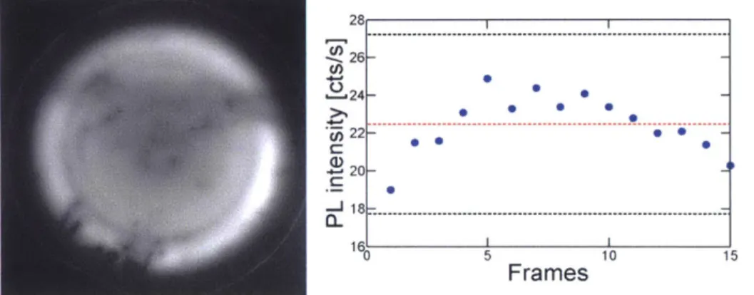
Figure 10: Photoluminescence variation measurements... 39
Figure 11: pt-XRF measurements along random-angle grain boundary ... 41
Figure 12: Fluorescence spectra at metal-rich particles... 41
Figure 13: Comparison of chromium- and iron-rich precipitates ... 42
Figure 14: Average lifetime and chromium point defect concentrations ... 44
Figure 15: Spatially resolved lifetime, chromium concentration, and iron concentration... 46
Figure 16: Wavelength dependence of photon absorption in c-Si... 51
Figure 17: Proposed setup for temperature- and injection-dependent lifetime spectroscopy... 53
Figure 18: Free carrier absorption measured at three different temperatures... 54 Figure 19: Extracting Shockley-Read-Hall lifetime as a function of temperature and injection lev e l...5 8
TABLES
CHAPTER
1
INTRODUCTION
1.1 Motivation: Cost, efficiency, and lifetime
Decreasing the cost of photovoltaic (PV) modules is a significant and urgent challenge. The PV industry has grown rapidly over the last 15 years: installed, grid-connected PV capacity grew from 1.3 GWP in 2000 to 139 GWP in 2014 [1]. Despite this rapid growth, solar PV accounted for less than 1% of the global electricity production in 2013. To reach 4,500 TWh per year installed PV capacity (11% global electricity production), projected by the International Energy Agency by 2050, current manufacturing capacity must be scaled quickly and cost-effectively [2]. Since area-dependent costs (e.g., module materials and installation hardware) scale inversely with module efficiency, one of the most effective ways to reduce the installed system cost is to increase this solar-to-electricity conversion efficiency [3], [4]. This is shown in Figure 1, reproduced from [5], where efficiency is located in the top right of the sensitivity plot.
Over 90% of the solar cells manufactured today comprise crystalline silicon. Single-crystalline silicon (sc-Si) held a market share of approximately 35% in 2014, while multicrystalline silicon (mc-Si) held a market share of approximately 55% [6]. Due to a simpler manufacturing process in which polysilicon is melted and re-solidified in a crucible, the area cost ($/m2) of mc-Si wafers is lower than that of sc-Si wafers which are typically made by the Czochralski crystal-pulling method. In 2013, the estimated manufacturing cost of a standard mc-Si module was US$0.92/W, with a minimum sustainable price of US$1.11/W, [5]. The minimum sustainable price tracks with the manufacturing cost and is a metric used to separate the market price from the finances of the manufacturer.
Sensitivity Map for 2012 Cost Structure 1 *Efficiency Yield .0 V Silicon Feedstock Depreciation w 0.1 C *Labor = .Metal Paste
-U 4Other Module Cost Components:
u * 1) Glass 7) Input Electricity
W_ 2) Wire sawing 8) JB and Cable
V *3) Frame 9) Encapsulant
E 4) Chemicals 10) Ribbon 5) Maintenance 11) Ingot Casting 6) Back Sheet 12) Screens
0.01 ---
-0 0.25 0.5 0.75
Maximum Cost Savings Available [US$/WI
Figure 1: Photovoltaic module cost sensitivity
This figure is reproduced from [5]. The module cost sensitivity is plotted versus the available cost savings to elucidate the most important parameters to reduce module-manufacturing cost. Efficiency, located in the top right
corner, is one of the most important levers to reduce the cost per peak watt.
A key innovation area in crystalline silicon is continued optimization of lower-cost materials, including mc-Si. The record research-scale solar cell efficiency for mc-Si is 20.8% in 2015, held
by Trina Solar, and the record efficiency for a sc-Si solar cell in 2015 is 25.6%, held by Panasonic with the Heterojunction with Intrinsic Thin layer (HIT) solar cell architecture [7].
Efficiencies of mc-Si solar cells are typically lower than sc-Si cells due to an abundance of metal impurities such as iron [8], [9]. In addition, the distribution of mc-Si solar cell efficiencies from
an ingot normally include a low efficiency "tail," which has in part been attributed to grain
boundaries and the multiplication of dislocations during growth [10].
A typical mc-Si solar cell configuration is shown in Figure 2 below. Incident light with energy above the bandgap of silicon (1.124 eV [11]) is absorbed to produce free carriers - one
electron in the conduction band and one hole in the valence band for each photon. A pn-junction separates these carriers into electrons and holes for extraction as usable current in the external
circuit, which can be electricity for a home, a business, or the grid. The solar cell conversion
circuit) to incident power (the number of photons approaching the module before any protective layers such as glass). In a simple approximation for silicon solar cells, free carriers near the junction are transported across by drift due to the electric field at the junction. Far away from the junction, diffusion due to concentration gradients determines free carrier motion. For separation to occur, free carriers must be allowed sufficient time after excitation to diffuse to the junction and then from the junction to either the front or back contact of the solar cell.
Front Contact Emitter External Bs load Back contact No Generation Recombination light
Figure 2: Diffused-junction multicrystalline silicon solar cell configuration
Schematic of a standard p-type mc-Si solar cell, with an n-type emitter produced by phosphorous diffusion. When light is absorbed by the solar cell, free carriers (electrons and holes) are produced. The pn-junction located between the emitter and base separates electrons and holes for extraction through the back or front contacts as usable current.
Figure adapted from [11].
Carrier separation and collection is often limited by non-ideal processes, during which carriers produce a photon that can be reabsorbed or recombine rather than reaching the external circuit. Recombination can take many different forms, as will be discussed in Chapter 2. In the presence of defects, depicted in the inset of Figure 2, recombination occurs after carriers are excited through an energy level located between the two bands. The amount of time that a carrier remains in an excited state before recombination is termed the "lifetime." In a p-type base, the dopant introduces a large number of holes into the material. As a result, holes are termed the "majority" carriers in this region, and electrons are termed "minority" carriers. Because majority carriers are abundant, the behavior of minority carriers limits the base lifetime. Minimizing recombination and therefore maximizing lifetime in the base material is essential for high
efficiency. PCi D [12] was used to model a simple solar cell like that shown in Figure 2 with parameters similar to those specified in Table I of [13]. The cell thickness was 180 pm. To assess the impact of lifetime on efficiency, the lifetime was varied between 0 and 300 ps and the efficiency at maximum base power was extracted. The results are plotted in Figure 3. At very low lifetimes (< 25 gs), efficiency increases linearly with lifetime. As lifetime increases past 100 ps, the efficiency begins to level off but still increases slowly with lifetime. This curve will be different for every solar cell configuration. For a solar cell with very low surface recombination velocities, low shunt resistances, and low contact resistances, small changes in base lifetime will have a more dramatic effect on efficiency.
1)
r-.-m18--U 17-
-10 50 100 150 200 250 300
Lifetime [ps]
Figure 3: Efficiency as a function of lifetime
Solar cell efficiency is plotted as a function of base lifetime. Simulations were performed using a diffused junction configuration in PC I D with one internal shunt element, front surface reflectance, internal reflectance, and other
parameters specified in [13].
The lifetime can also be expressed as a diffusion length using the following relation:
LD=Vt
H
(1
where D is the diffusivity of the carrier at the solar cell operating temperature and r is the carrier lifetime. The diffusion length is an important metric for intuitive understanding of solar cell operation: if the distance between the excited free carrier and the junction is much greater than the diffusion length, the probability for carrier collection will be low. If the carrier diffusivity is known, which is not always the case in novel materials, the diffusion length can be easily
calculated from a lifetime measurement. In this thesis, I will focus on the lifetime rather than the diffusion length, but it is important to remember that the two terms are closely related.
Metal impurities such as chromium and iron act as minority-carrier recombination centers through mid-gap energy states, limiting charge-carrier lifetimes at device-relevant excess-carrier densities [14], [15]. These metal impurities can be present as either single atoms within the lattice (interstitial or substitutional and especially detrimental) or precipitates. The impact of
different metal impurities on solar cell efficiency has been studied through experiment and simulation with the conclusion that low concentrations of impurities can significantly degrade efficiency [16]-[18]. To prevent solar cell performance degradation by impurities, two approaches exist: 1) root-cause elimination and 2) management through gettering. In the first approach, the contaminant and its source must be identified. Chromium, for example, is a major component of stainless steel, which is often used in wafer-fabrication equipment. If stainless steel components are removed from the process, the amount of chromium contamination should decrease or become undetectable. Engineering impurity distributions through high-temperature gettering processes is an alternative approach when the root cause cannot be completely eliminated or when root-cause elimination is prohibitively expensive. There is some background contamination in the crucible material used to grow mc-Si ingots that cannot be removed - high-temperature gettering during phosphorous diffusion can reduce the impact of contaminants in this case.
Knowledge of the thermodynamics and kinetics of a contaminant can inform diffusion gettering profile design to mitigate the impurity impact on solar cell efficiency. Iron, for example, has been well-studied, and kinetics process simulation tools exist to engineer its distribution in the material [19]-[23]. In contrast, the impact of processing steps on chromium (both precipitated and interstitial) has not been studied as extensively, although the detrimental nature of the impurity is well-known. Interstitial chromium (Cri) is highly effective at capturing minority carriers: the capture cross-sections for chromium are 1.5 and 57 times larger than iron in p- and n-type silicon, respectively [18]. Chromium has been found to impact cell performance at concentrations as low as 1010 cm-3, and the maximum allowable chromium contamination in the silicon melt ranges from lx 1015 cm-3 to 2x 107 cm-3 depending on the crystal growth method, device architecture, and target efficiency [17], [24], [25]. In this thesis, I will explore the gettering response of chromium impurities in mc-Si.
1.2 Prior work on Cr impurities in Si
As lifetimes of industrial materials have improved, interest in studying transition metal contamination in silicon has increased. Though not as omnipresent as iron, chromium has appeared in moderate concentrations in industrial samples [9]. Conzelmann et al. [26] presented one of the first studies regarding recombination due to chromium impurities in silicon. A defect level at 0.23 eV below the conduction band was attributed to interstitial chromium, while a distinctly different level at 0.27 eV above the valence band was attributed to chromium-boron pairs in p-type silicon [26]. Later, the defect parameters of chromium were refined through measurements by a variety of different techniques, including surface photovoltage, deep-level transient spectroscopy, and temperature- and injection-dependent lifetime spectroscopy
[27]-[31]. Habenicht et al. [30] produced spatially resolved images of chromium point defect
concentration in mc-Si samples by controlling the defect state and adapting the methods for iron point-defect measurements first proposed by [32].
At sufficiently high contamination levels and for a range of doping concentrations, chromium ions are favored to form precipitates. Bendik et al. [33] used electron paramagnetic resonance measurements to study the precipitation kinetics of intentionally chromium-contaminated silicon. Formation of chromium disilicide (CrSi2) precipitates during crystallization has been confirmed by energy dispersive X-ray spectroscopy [34]. In mc-Si, precipitation at dislocations during
cool-down after crystallization was predicted by numerical simulation [35] and implied by micro-photoluminescence techniques [36]. Sch6n et al. found that minority carrier lifetime increased and [Cri] decreased after phosphorous diffusion gettering [35]. Other quantitative studies of the effect of phosphorous diffusion gettering have measured high chromium concentrations at near-surface regions, suggesting external gettering [37]-[39], as well as a reduction of the total bulk chromium concentration [40].
1.3 Approach
In this thesis, I hypothesize that the distribution of chromium in silicon can be engineered in a similar manner to iron by high-temperature processes. Chapter 2 contains important background information regarding minority carrier lifetime measurements, the nature of impurities in silicon, and impurity detection techniques. In Chapters 3 and 4, I employ synchrotron-based X-ray
fluorescence microscopy to study chromium distributions in multicrystalline silicon in as-grown material and after phosphorous diffusion. Interstitial chromium concentration and minority carrier lifetime measurements complement quantified precipitate size and distribution to provide insight into chromium gettering kinetics and offer suggestions for minimizing the device impacts of chromium. The quantitative data provided through this work can be used to inform future studies of the gettering kinetics of Cr in silicon, assumed to be the same in both n- and p-type silicon at solar cell processing temperatures.
During the course of this research, I have learned that detecting impurities in low concentrations in photovoltaic materials is a pressing challenge to maintain the current pace of innovation. The techniques employed in this thesis are limited to precipitated metals or specific impurities in p-type silicon at concentrations around 1010 cm-3. Multicrystalline silicon in
industry today is well-suited to these characterization techniques due to the high dislocation density and background contamination levels; however, as the industry considers a transition to solar cells with high-purity and/or n-type base materials, more sophisticated characterization techniques are required. In Chapter 5, I present a concept for a new defect characterization tool that utilizes minority carrier lifetime as a response variable.
CHAPTER
2
THEORY OF IMPURITIES AND
IMPURITY DETECTION
Given the importance of mitigating the detrimental impact of metal impurities, the following sections present the relevant theory regarding lifetime, impurities and impurity detection techniques. Throughout this chapter, it is assumed that the material is uniform and isotropic, that the semiconductor is non-degenerate crystalline silicon, and that measurements are taken when the sample is in thermal equilibrium. Other assumptions are stated explicitly throughout the text when required.
2.1 Carrier lifetime
Minority carrier lifetime is generally accepted as an indicator of the efficiency potential of a wafer prior to processing into a full solar cell. Above-bandgap light incident on a solar cell is absorbed to excite electron-hole pairs. After this light is absorbed, the electrons and holes must diffuse to their respective contacts (such as the fingers, bus bars, and back contacts of a typical solar cell) to generate current. Because diffusion is not instantaneous, but instead governed by the diffusion coefficient of an electron or hole at the solar cell operating temperature, the carriers must remain in an excited state for a certain amount of time to ensure collection. The carrier lifetime is a measure of the time that electrons and holes remain in this excited state. In doped bulk material, the lifetime of minority carriers (electrons in p-type material and holes in n-type material) is typically the limiting factor due to the excess of majority carriers.
Lifetime can be expressed analytically as a function of excess minority carrier density, the rate of change of the excess minority carrier density, and the generation rate [41]:
An
G - dAn/dt
where G is the generation rate and An the excess minority carrier density in p-type material. The generation rate is defined by the number of electron-hole pairs generated by incident photons and can be expressed as follows [42]:
G(A,x) = a(A)Noexp(-a(A)x) (3)
where a is the optical absorption coefficient as a function of photon wavelength (. ), No is the
number of incident photons per unit area per unit time, and x is the depth into the material. The above equation assumes that the absorption coefficient is independent of position in the material and that absorption is governed by Beer-Lambert's law. In a typical lifetime measurement, the excess carrier density is monitored as a function of time and the generation is either known, measured simultaneously, or can be ignored in the case of high lifetime.
Lifetimes are discussed in terms of the injection level, which is formally defined as the ratio of excess to equilibrium carriers [43]:
An
Injection Level = (4)
no + po
where no and po are the equilibrium carrier concentrations. Low-level injection is defined as the case when the number of excess carriers is small compared to the equilibrium carrier concentrations, typically An z 1014 cm-3 for standard solar materials with doping levels on the
order of 1016 cm-3. High level injection is the opposite case, with An z 1018 cm-3. In this thesis, I
will discuss the absolute injection density rather than the normalized injection level. A typical solar cell such as that depicted in Figure 2 operates at maximum power point in low injection,
between 1012 cm-3 and 3x 10 cm-3 according to simulations [44]. The injection level is
dependent on the solar cell architecture and conversion efficiency. For example, a more advanced solar cell with carrier-selective contacts can operate closer to 5 x 1014 cm 3 [44].
The apparent, or measured, lifetime of any semiconductor material is the result of competing recombination mechanisms. This apparent lifetime can be expressed as a harmonic sum:
1 1 1 1 1
Tmeas = d+ + + + (5)
TRad TAuger TSRH TSurf Tother
The first two terms in the above equation, radiative (Rad) and Auger, correspond to what is typically classified as the intrinsic lifetime in silicon. In the case of highly doped silicon or
dominant impurity interactions, however, Auger recombination may no longer be considered an intrinsic mechanism. The third term, Shockley-Read-Hall (SRH), represents recombination through defect centers within the bandgap of the material. The fourth term is associated with recombination at the surfaces of the semiconductor. These mechanisms corresponding to the first four terms are discussed in detail in the following sections. The last term is associated with any other, unaccounted-for recombination mechanisms (e.g., recombination at precipitates if not represented by the SRH statistics).
2.1.1 Radiative recombination
Radiative recombination occurs when an electron and a hole recombine band-to-band and emit a photon of equivalent energy. In an indirect bandgap semiconductor such as silicon, radiative recombination must also involve a phonon, making it less likely to occur than the other recombination mechanisms. For a sample in thermal equilibrium, the radiative lifetime can be expressed as [45]:
noPo
TRad = (6)
B(T)nm(no + po)
where B is the radiative recombination coefficient and ni is the intrinsic carrier concentration. The radiative recombination coefficient is equal to 2x 10-15 cm3/s at room temperature [45]. This
coefficient changes with sample temperature: as temperature increases, the coefficient decreases. An expression for B can be derived from the generalized Planck equation for spontaneous emission from band-to-band transitions as a function of temperature and photon energy [46]:
1 (hw)2
-n hw
B(hw, T) = -12 - aBB(h, T) ' exp(- ) (7)
n? _n2h3C2 kBBT
where o is the photon frequency, n is the index of refraction, aBB is the energy- and temperature-dependent band-to-band absorption coefficient, T is the sample temperature, and kB is the Boltzmann constant. To obtain the B coefficient at a particular temperature, Equation (1) must be integrated over the entire spectrum. Several studies have shown this dependence experimentally. The authors of [47] fit a 5th order polynomial to historical experimental data to allow quick extraction of the B coefficient at arbitrary sample temperatures.
2.1.2 Auger recombination
Auger recombination involves three free carriers - either two holes and one electron or two electrons and one hole. One electron-hole pair recombines band-to-band, but rather than emitting a photon, the energy associated with the transition is transferred to a third carrier that is promoted to an excited state within its original band. Traditional models for Auger recombination assume that the carriers are quasi-free and do not interact [48]-[50]; more recent models, which agree more closely with experimental data, account for interactions due to Coulombic attraction/repulsion [51], [52], phonons [53], and impurities [54]. Combining radiative and Auger recombination, the following expression is an advanced parametrization of the intrinsic lifetime in silicon [55]:
Tintr,adv
An (8)
(np - nI)(2.5 x 1- 3 19eehno + 8.5 x 10- 3 2gehhpo + 3.0 x 10⁻² 9An0.92 + BreiBiow)
where ni, no, po, and An are as defined previously; n and p are the total electron and hole densities; geeh and gehh are functions of the equilibrium carrier concentrations, defined in [55];
Blow corresponds to the radiative recombination coefficient for lowly doped and lowly injected silicon (4.73x10 15 cm3s-1 [46]), and Brei is defined according to [56]. This expression, use to
calculate intrinsic lifetime throughout this thesis, accounts for Coulomb enhancements and is valid at room temperature for bothp- and n-type silicon across the injection range.
2.1.3 Shockley-Read-Hall recombination
Shockley-Read-Hall (SRH) recombination occurs through a defect center located somewhere in the bandgap. As will be discussed in Section 2.2.2, SRH recombination is representative of recombination at most metal point defects in silicon. A trap, or defect center, can affect the recombination rate by capturing or emitting an electron and/or hole to or from its respective band. The formalization of the SRH lifetime is based on the statistical probabilities of the different recombination processes [14], [15]. When An = Ap (for small defect concentrations),
the SRH lifetime is defined as follows:
TSRH =no(po + Pi + An) + Tpo(no + n, + An) (9) nR + Po +An
Tno ' = (Ntc 1 th) 1; Tp0 = (Ntcpthj' (10)
(_E_-_E
Et -Evnj = NC exp - ;t p, = Nyexp(-E ) (11)
kBT kBT
where rno and rpo are termed the electron and hole capture time constants; an and up are capture cross-sections for electrons and holes for a particular defect; Vth is the thermal velocity of carriers
(Z I x 107 cm/s for both types); Nc and Nv are the effective densities of states in the conduction
and valence bands; and E, is the energy of the defect level with respect to one of the band edges. The above expression assumes that trapping at defect centers is negligible and does not affect the lifetime (i.e., An ~ Ap), the defect level is stable within the bandgap, and the impurity concentration is not so high that it affects the background doping concentration [41]. If more than one SRH defect is present, the individual SRH lifetimes are combined by harmonic sum to determine a total SRH lifetime. The SRH lifetime can also be written in terms of the ratio of electron-to-hole capture cross-sections, k. This form of the equation reduces the number of unknown fitting parameters when lifetime spectroscopy is used for defect identification.
2.1.4 Surface recombination
Surface recombination most often occurs as a result of dangling bonds at the surface of the wafer. These discontinuities may present as Shockley-Read-Hall recombination centers, but surface recombination lifetime is typically characterized in terms of the surface recombination velocities (SRV, measured in cm/s) at the front and back surfaces of the wafer. When the two SRVs are equal, an approximation for the surface lifetime is as follows [57]:
W 1 W) 2
Tsurf ~ - -- (2
2S D 1T
where S is the SRV, W is the wafer thickness, and D is the diffusivity of the minority carrier in the material.
The SRV depends, among other things, on the passivating layer material, the deposition conditions of the passivating layer, and doping type and concentration of the wafer. Aluminum oxide (AlOx), for example, is deposited by atomic layer deposition and is known to be an effective passivating layer for p-type materials due to a fixed negative charge that repels minority carriers from the surface, resulting in an effectively low SRV due to the absence of minority carriers [58], [59]. This type of passivation mechanism is termed "field effect." A passivating
layer may also reduce the number of trap states at the surface (Dit) to achieve a lower SRV. This is termed "chemical" passivation. For effective passivation (low SRV), a layer should have both field effect and chemical passivation mechanisms [60].
For the purposes of this thesis, the passivation layer employed is AlOx, with a surface recombination velocity on the order of 10 cm/s. The SRV is estimated when necessary by passivating a high quality float-zone control wafer of similar resistivity to the samples of interest. The measured lifetime of the control sample is assumed to be equivalent to the harmonic sum of the intrinsic lifetime (8) and the surface lifetime (12).
2.1.5 Contributions to measured lifetime
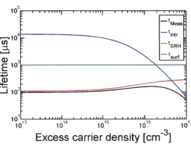
Figure 4 below displays the breakdown of the different lifetime mechanisms in the case of
1016 cm3 p-type doping with a single Cri-Bs defect center with a concentration of 5x 101 cm-3
(calculated according to the SRH statistics, discussed in Section 2.1.3). The SRV (discussed in the previous section) is taken to be 10 cm/s and constant with injection level. The lowest lifetime among the different recombination mechanisms will dominate the measured lifetime. In silicon, the intrinsic mechanisms, including radiative and Auger, represent the maximum lifetime of the material. If the measured lifetime is equal to the intrinsic lifetime, no further improvements to the material can be made. To isolate a particular mechanism from the measured lifetime, the quantities of the other mechanisms must be known or negligible. In the case of highly contaminated material, for example, the SRH lifetime is typically much lower than the intrinsic lifetime or surface lifetime. The measured lifetime can be considered to be a close approximation to the SRH lifetime. The goal throughout this thesis is to extract and analyze parameters relevant to the SRH lifetime.
In -Mes -10 -ntr _SRH _) srf Ej 10O3 102* 1. 1 13 14 1 11115 1 & id16 1 1 17 10 10 10 10 10
Excess carrier density [cm-]
Figure 4: Breakdown of recombination mechanisms
Recombination mechanisms contribute to the overall measured lifetime of a theoretical sample. The sample has a p-type doping level equal to 1016 cm~3, a concentration of Cri-B, defect centers equal to 5x 1010 cm3, and an
injection-independent surface recombination velocity of 10 cm/s. In low injection, the lifetime is dominated by SRH recombination, while in high injection, the intrinsic lifetime governs the measured lifetime.
2.1.6 Lifetime measurement techniques
Common techniques used to measure carrier lifetime in silicon include photoconductance decay, free-carrier absorption, and photoluminescence. Both Sinton Instruments and Semilab offer tools to measure photoconductance decay. The Sinton Instruments WCT-120 is widely used throughout the industry and consists of a flash lamp, a calibrated light sensor, and an RF coil. The sample is placed on top of the RF coil, which measures 40 mm in diameter; when the sample is flashed with the broadband light source, excited carriers induce a voltage in the RF coil that is recorded as a function of time. The light sensor on the tool serves to measure the incident photon flux. Depending on the sample lifetime, the measurement can be performed in
quasi-steady-state (QSS, T < 200 gs, dAn/dt -> 0), transient (r > 100 ps, G -> 0), or generalized (any
lifetime, both terms) mode. The output data consists of the apparent lifetime across the measured
injection range (typically 101-1011 cm3). [61]
The Semilab WT-2000 performs a point-based transient lifetime measurement of microwave photoconductance decay (MW-PCD), rastered in x and y across the sample surface. Unlike the WCT-120, the WT-2000 uses a single wavelength (905 nm) to excite carriers and a microwave antenna (10 GHz) to measure reflected microwave power after excitation. The microwave power
is a function of the sample conductivity and therefore the excess carrier density. A time constant is fitted to the measured time-dependent decay curve at each (x, y) location on the sample, and a spatially resolved lifetime map is produced. While the generation rate across the sample is constant in this setup, the injection level may vary based on the underlying injection-dependent lifetime curve and must be estimated separately at each pixel. [62]
Similar to photoconductance decay, free-carrier absorption (FCA) is a transient measurement of the time-dependent carrier density in the material after an excitation pulse. In an FCA measurement, carriers are pumped into the material with a laser pulse greater than or equal to the bandgap of the material (1.124 eV for silicon) while transmission of a continuous wave probe beam with an energy much less than that of the bandgap is measured as a function of time. Carriers that are already in an excited state in either the valence or conduction band will readily absorb low-energy light. The FCA coefficient is proportional to the excess carrier density. Assuming uniform generation throughout the sample thickness, Beer-Lambert's law can be used to relate the transmitted light intensity to excess carrier density and eventually to lifetime. Like the WCT-120, FCA provides injection-dependent lifetime data. Though it is a point-based measurement, the technique can be implemented with a rastering mechanism to produce spatially resolved information. [63]
Photoluminescence (PL) can be performed as a transient pump-probe optical measurement (similar to FCA) or as a QSS measurement using a CCD camera. In the transient approach, carriers are pumped into an excited state and the lifetime is measured according to the intensity of the luminescence signal that corresponds to the amount of radiative recombination occurring in the material. In the QSS approach, widely used for silicon lifetime measurements, the sample is uniformly illuminated with a single wavelength above the bandgap of the material while a
CCD camera captures luminescent photons as a function of spatial position. The measured
luminescence intensity must be calibrated to the excess carrier density or the lifetime of the material. Several methods, including calibration by photoconductance [64] and self-consistent calibration with a specialized detector [65], have been defined to convert the luminescence intensity to lifetime for the QSS measurement. As with MW-PCD, the generation rate across the sample is constant while the measured injection level may vary. To specify the entire injection-dependent lifetime curve, images must be taken at a range of different illumination laser powers and then stitched together pixel-by-pixel.
2.2
Metallic impurities
Metal impurity contamination of solar cells can occur at any point throughout the manufacturing process, but contamination is most likely to occur during high temperature steps
(e.g., during crystal growth) when impurities are highly mobile. Transition metals are known to
form mid-gap levels within the bandgap of silicon, affecting bulk lifetimes at low concentrations. The diffusion length of an impurity is related to its diffusivity and the duration of the high temperature step as follows [66]:
L = dD(T)t (13)
where L is the diffusion length, D is the temperature-dependent diffusivity of the impurity, and t is the duration. Given a sufficient surface contamination on a wafer, for example, the affected volume of material is related to the diffusion length during processing. As explained in [66], three cases are possible given a high concentration of mobile impurities: 1) Precipitates of impurity atoms form within the bulk; 2) Precipitates of impurity atoms form near the wafer surface; or 3) Impurity atoms remain in dissolved form throughout the material. In the following sections, I will discuss cases (1) and (3), which are most common for transition metal impurities.
2.2.1 Precipitated metals
Precipitate nucleation can occur homogeneously (i.e., throughout a single crystalline material) or heterogeneously at structural defects. In as-grown multicrystalline material, it has been shown experimentally that metal precipitate nucleation is favored at bulk heterogeneous nucleation sites
[9], [67], [68]. Metal precipitation occurs at a certain critical level of impurity super-saturation,
which is a function of temperature, concentration, solubility, diffusivity, nucleation site density, and nucleation energy barrier [66], [69]. The solubility and diffusivity of a particular impurity are functions of temperature [66]:
s=
So exp - (14)
(kB kBT
D = Doexp(- M (15)
kBT
where So and Do are temperature-independent coefficients, Ss is the solution entropy, Hs is the solution enthalpy, and HM is the migration enthalpy. With knowledge of precipitation kinetics,
precipitate size and distribution can be engineered through design of time-temperature profiles for phosphorous diffusion gettering (Section 2.4).
Since precipitates tend to be located at structural defects such as grain boundaries, it is difficult to separate the effects of the different mechanisms on minority carrier lifetime or diffusion length. With careful sample preparation, the authors of [70] were able to form NiSi2
precipitates without other defects and fit their results with an a coefficient of 0.7 to the following equation for the carrier diffusion length:
LD = aN-3 (16)
where a is a constant that depends on the specific defect and N is the defect concentration. An alternative approach defines the lifetime due to metal precipitates to be a form of the SRH equations under low injection, where the capture cross-section, concentration, and thermal velocity of the defect are related to the spherical precipitate size and density (r, N), the
recombination velocity at the precipitate surface (s), and the minority carrier diffusion length (D) [20], [71]:
= 2 NsDr (17)
Tprec s + Dir
A Schottky effect model has been proposed to further refine the description of recombination at
metal precipitates by accounting for band-bending at the precipitate surface [72]. Precipitate recombination is an area of ongoing research and is not the subject of this thesis. This thesis focuses on recombination at metal point defects (next section), but it is important to recognize that precipitated metals can also contribute to the total recombination rate in the material.
2.2.2 Metal point defects
Metal point defects can be either interstitial (between lattice sites) or substitutional (sitting on a lattice site). Dopant atoms, for example, are a form of substitutional impurity that sits directly on a silicon lattice site. The material's resistivity is decreased by their addition because the dopant atoms typically have one less or one more electron than a silicon atom. The energy levels of phosphorous and boron, common dopant impurities, lie very close to the conduction and valence bands, respectively, so that they are easily ionized at room temperature. Metal impurities, when present in concentrations on the order of the dopant concentration, can contribute in a similar way to the intrinsic carrier concentration. In industrial materials, this is
typically not the case as dopant levels for photovoltaic materials are ~l016 cm-3 while impurity
levels are 1014 cm~3 or less.
A metal point defect can be uniquely characterized by its energy level with respect to one of
the band edges and its capture cross-sections for electrons and holes. Recombination at transition metal point defects can then be modeled by the SRH statistics, as explained in Section 2.1.3. Common metal impurities that limit performance in photovoltaic materials include iron (Fe), chromium (Cr), copper (Cu), and nickel (Ni). The effect of these impurities on solar cell performance has been studied both experimentally [16], [25] and through simulation [17], [18]. 2.2.3 Chromium
Chromium (Cr) is known to be a detrimental impurity in silicon, affecting solar cell performance at concentrations as low as 1010 cm-3 [16]-[18]. In interstitial form, chromium acts
as a highly effective recombination center in both p- and n-type silicon. Compared with iron, the minority carrier capture cross-sections for chromium are 1.5 and 57 times larger in p- and n-type silicon, respectively. Interstitial chromium (Cri) forms at donor level at 0.24 eV below the conduction band, with a capture section for holes of 4x10-" cm2 and a capture cross-section for electrons of 2x 104 cm2 [30]. In p-type materials, Cri forms a metastable pair with substitutional boron (Bs). At room temperature, Cri donates its electron to the conduction band to become positively charged, while Bs accepts an electron to become negatively charged.
Coulombic attraction causes a defect complex (Cri-Bs) to form which is dominant under standard solar cell operating conditions. The Cri-Bs formation and dissociation kinetics equations are not reproduced here but explained by Equations (I)-(10) in [30]. Cri-Bs forms a donor level at 0.27 eV above the valence band with a capture cross-section for holes of lx 10-14 cm2 and a capture cross-section for electrons of 2x 10-14 cm2 [30]. Chromium also forms precipitates in silicon and has previously been observed by energy dispersive X-ray spectroscopy to form chromium disilicide (CrSi2) [34]. This spherical precipitate consists of three Cr atoms in a hexagonal
configuration with a unit cell volume of 3.61 x 10⁻²³ cm3 [73], [74].
2.2.4 Iron
Iron (Fe) is another important impurity in crystalline silicon whose kinetics have been relatively well-studied. Interstitial iron (Fei) forms a donor level located 0.38 eV above the
valence band, with a capture cross-section for holes of 7 x 1017 cm2 and a capture cross-section
for electrons of 1.3x10 cm2 [8], [18], [75]. The resulting defect level is highly asymmetric, with a k value of 185. Similar to chromium, Fei forms a metastable pair with Bs. Upon illumination or heating, Fei and Bs are separated; left in the dark at room temperature, the two atoms will form Fei-Bs. Details regarding preparation of the two states can be found in [32], [75], [76]. Fei-Bs forms a donor level at 0.26 eV below the conduction band, with a capture
cross-section for holes of 3 x 10-" cm2 and a capture cross-section for electrons of 5 x 10-15 cm2 [18], [77]. Iron forms spherical iron-silicide precipitates (FeSi2) with unit cell volume equal to 3.76x10⁻² cm' [78].
2.3 Impurity detection techniques
It is important to be able to detect and characterize defects in solar cell materials to design mitigation steps such as phosphorous diffusion gettering (Section 2.4). In general, the goal is to identify the defects in a non-contact, non-destructive manner such that the response of the defect to different processes can be studied, that a solar cell could be made from the material, or even that the measurement could be performed in-line during manufacturing. Destructive techniques exist which work well to identify defects when present in high concentrations, including
Inductively-Coupled Plasma Mass Spectrometry (ICPMS) and Secondary Ion Mass
Spectrometry (SIMS). Electrical techniques such as Electron Beam-Induced Current (EBIC) and Deep-Level Transient Spectroscopy (DLTS) require the formation of a diode on the sample surface and can be complicated in analysis.
2.3.1 Micro-X-ray fluorescence
Synchrotron-based X-ray fluorescence (p.-XRF) is a non-destructive technique that has proven useful to probe transition metal precipitate distributions in silicon [9], [21], [67], [68]. The measurement involves high energy X-rays that excite core shell electrons in the sample material. As these excited electrons relax back to their resting states, corresponding photons are emitted and measured by a detector. The emitted fluorescence as a function of energy forms a spectrum that can be analyzed for chemical composition. In the studies presented in this thesis, the measured fluorescence corresponds to the Ka transition of the impurity. When XRF is implemented at a synchrotron with an x-y positioning stage, high-resolution spatially resolved
maps of chemical composition can be produced. Elemental detection depends on the absorption and fluorescence edges relative to the incident beam and detector capabilities. The beam energy used for this thesis is 10 keV, so that any element with an absorption edge at or below that energy can theoretically be detected.
For each sample measured at the beamline, long-duration, single-point p-XRF measurements of NIST standard reference materials 1832 and 1833 are used to quantify the background level. The minimum detection limit (MDL) of the technique is calculated according to the following equation, based on [67]:
3 IBkgd
MDL = X PElement,Std X A X v (18)
IStd
where MDL is measured in detectable grams for a particular element, PElement,Std is the areal
density of the element of interest in the NIST standard reference material (g/cm2), A is the
full-width half-maximum beam spot size (cm2), and t is the actual measurement time for the standard
material. The IBkgd and IStd terms correspond to the background or noise-related fluorescence and fluorescence from the standard reference material. These terms are calculated by fitting the fluorescence energy spectrum and calculating the area under the curve associated with the element of interest. The quantity 3VIBkgd represents the estimated noise level of the measurement. A similar equation is used to quantify spatially resolved p-XRF maps, with the background term replaced by the measured fluorescence at a particular pixel.
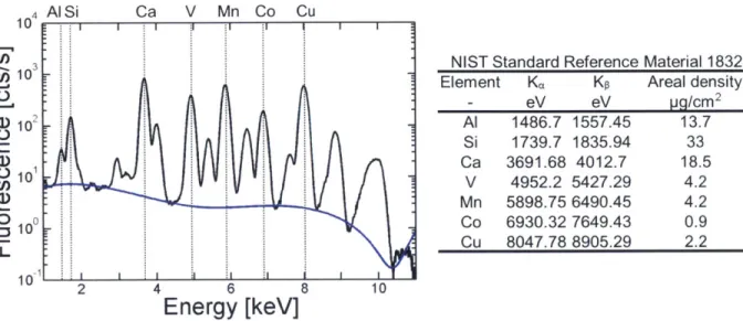
An example of a fluorescence spectrum from the 1832 reference material is shown in Figure
5. The table on the right in the figure lists the elements that are included in 1832. Reference
material 1833 contains Si, K, Ti, Fe, Zn, and Pb. The elements in the standards represent most elements of interest for silicon solar cell contamination. For elements that are not included, such as chromium, the MDL can be interpolated from measurements of the nearest elements on the periodic table. For chromium, these elements are vanadium (V) and manganese (Mn).
4 Al Si Ca V Mn Co Cu 10 . 3 10 j2 10 4--0 010 0 0
NIST Standard Reference Material 1832
Element Ka Kp Areal density
- eV eV pg/cm2 Al 1486.7 1557.45 13.7 Si 1739.7 1835.94 33 Ca 3691.68 4012.7 18.5 V 4952.2 5427.29 4.2 Mn 5898.75 6490.45 4.2 Co 6930.32 7649.43 0.9 Cu 8047.78 8905.29 2.2 2 4 6 8 10
Energy [keV]
Figure 5: Fluorescence energy spectrum of NIST standard reference material 1832
A sample fluorescence spectrum from NIST standard reference material 1832 is shown (left). The blue solid line is
an example of a fitted background curve. The vertical dotted lines correspond to the K, fluorescence energy for each of the elements included in the standard. The MDL is calculated by estimating the area under the plotted curve for a particular element. The fluorescence energies and areal densities for the standard reference material are shown in the
table (right).
The minimum detection limit in grams is converted to detectable Cr atoms according to the following equation:
atoms MDL [g] atoms
x NA[ ] (19)
precipitate Atomic weight Cr [ V] mol(
where NA, is Avogadro's number.
2.3.2 Metastable defect lifetime spectroscopy
Another group of techniques that will be employed throughout this thesis is based on extracting and analyzing the SRH lifetime of a given material. As mentioned in Section 2.2.3, chromium forms a metastable defect complex with substitutional boron in p-type silicon. Similarly, both iron and oxygen form metastable defect complexes in p-type silicon. With knowledge of the formation kinetics and defect parameters of these complexes, lifetime measurements in the associated and dissociated states can be used to extract the chromium, iron, and/or oxygen concentration in the material [27], [30], [32], [75], [76], [79]. If the two states are
and State 2 consists of a large fraction of Cri-Bs and a small fraction of Cri), the following series of equations can be used to determine the concentration of the defect N of interest:
[N]= C(An)[- (20)
[1
1 1 C (An) f21 ) xN-B + (1- N 2 - 2)XN-B N,N-B _ VthUn(NA + ND + An) 12 NA + p, + An + k(ND +n+An)(where
f,
andf
2 relate to the fraction of Ni or Ni-Bs in either state, X is derived from the SRHlifetime equations for the particular defect, NA and ND are the acceptor and donor dopant concentrations, and all other parameters have been previously defined. The exact formation of Equations (20)-(22) depends on the injection level of the measurement and the relative lifetimes of the defects at that injection level. For example, in low-level injection, the SRH lifetime due to Fei-Bs pairs is higher than the SRH lifetime due to Fei point defects, so that r1 would correspond to Fei and r2 to Fei-Bs. In high-level injection, the lifetime trend is switched. The detection limit for such a technique can be as low as 109 cm-3, but this is dependent on the injection level,
lifetime, defect, and precision of the lifetime measurement. To produce a reliable measurement, the defect states must be controlled so that the fraction of each defect in States 1 and 2 is known with high precision.
2.3.3 Generalized lifetime spectroscopy
Lifetime spectroscopy can also be applied more generally to silicon materials for defect identification. Given an injection-dependent lifetime curve, the SRH lifetime can be extracted with knowledge of the intrinsic and surface lifetime components, as explained previously. Each defect, characterized by its concentration, energy level and capture cross-sections, presents a unique signature in terms of the SRH lifetime magnitude and injection-dependent shape. One approach to extracting the defect parameters from an injection-dependent curve is linearizing the SRH equation [80]:
l1 flnip Qn1 i1
TIn 1+ +-+X
(
Q-- (23)ac Nt Po Po Po Po
where an is the electron capture coefficient of the defect (an X Vth from the SRH lifetime),
Q is the
ratio of electron capture coefficient to hole capture coefficient, and X is a revised independentparameter (X = n/(po + n)). Equation (23) is written for the case with one dominant defect in
p-type material, but similar equations can be written for multiple defects and for n-type material.
A set of experimental SRH lifetime data is plotted versus the normalized injection level X to
reveal the nature of the defect or defects. If one defect is dominant, the plot will show a linear line with a slope and intercepts that are related to that defect. If multiple defects are dominant, the plot will exhibit some curvature or a slope that relates to the harmonic sum of the two defects. An example of this linearization in the case of simulated SRH lifetimes is shown in Figure 6 below. The defect parameters are extracted by analyzing the slope and intercepts of the linear line or linear fits to the curve in the case of multiple defects, as explained in detail in [80].
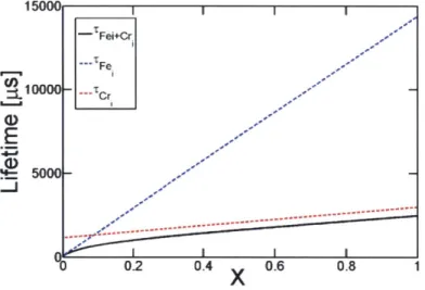
15000
- Fei+Cr
=L 10 - C
-0.2 10.4 X 0.6 0.8 1
~X
Figure 6: Shockley-Read-H all linearization for defect analysis
The linearized SRH lifetime is plotted for a p-type sample with 101 CM-3 Cri and 1011 CM- Fei. The y-axis of the graph is the lifetime, while the x-axis is the normalized injection level defined in the text. The doping level of the
sample is 1016 CM-3 . The overall lifetime curve (black solid line) has a slight curvature with respect to the x-axis, which indicates the presence of two lifetime-limiting defects. If the sample contained only Cri or only Fei, the
lifetime curve would be linear as shown by the red and blue dashed lines, respectively.
Extensions of lifetime spectroscopy involve analyzing the temperature and doping
dependence of the lifetime either simultaneously or in addition to the injection-dependent
analysis. Temperature-dependent lifetime spectroscopy (TDLS) measures the low-level injection lifetime as a function of temperature. In low-level injection (LLI), as was shown qualitatively in Figure 4, the measured lifetime is typically dominated by SRH recombination if a defect is
valid for a particular sample, extraction of the SRH lifetime can be performed as explained previously with knowledge of the other recombination mechanisms. The temperature-dependent LLI lifetime is then plotted on an Arrhenius plot (log(CLLI/T) v. 1000/T). The slope of the linear increase of the plotted curve is equal to the defect energy depth; a fit to the entire curve, including the linear increase and some non-linear portion of the curve, yields the bandgap half.
[41]
Doping-dependent lifetime spectroscopy (Ndop-IDLS) and temperature- and injection-dependent lifetime spectroscopy (TIDLS) are more advanced approaches to probing the defect parameters. The SRH lifetime is measured at either different doping levels or different temperatures, both of which affect the SRH formalization (9) in known and predictable ways. By fitting each injection-dependent curve independently for the defect parameters and then analyzing the trends across doping level or temperature, the defect can be specified unambiguously in terms of Et, k (the ratio of capture cross sections), and TnO or TpO (10). The
challenge of implementing Nd0p-IDLS is sample fabrication. For robust analysis, the defect
population between samples must be identical while only the doping level is varied. This is difficult unless, for example, the doped wafers can be grown directly from the melt or from gas and process conditions can be closely controlled. TIDLS and its practical application will be discussed in more detail in Chapter 5. [41]
2.4 Impurity gettering by phosphorous diffusion
Gettering is a method of engineering the distribution of metal impurities to improve solar cell performance. Graff defined gettering to be a temperature-dependent process in which "unwanted metal impurities" are redistributed such that their impacts on device performance are minimized
[66]. In this thesis, I will focus on gettering during phosphorous diffusion, a process step used to
form the highly doped n-type emitter layer of a diffused junction p-type silicon solar cell. The high temperatures and times required during phosphorous diffusion compared to other solar cell processing steps provide an opportunity to manipulate and redistribute metal impurities as Graff suggests. Phosphorous diffusion gettering (PDG) has also been shown to be effective for n-type materials, improving lifetime over two orders of magnitude [81].
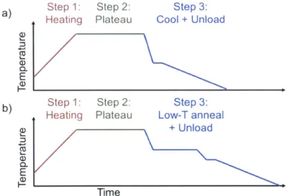
A typical PDG process consists of three steps, as depicted in Figure 7. In the first step