Development of Low-Temperature Solution-Processed Colloidal Quantum Dot-Based Solar Cells
by
Liang-Yi Chang
B.S. Materials Science and Engineering National Tsing Hua University, 2005
ARCHIVES
MASSACHUSETS 1N57 y f OF TECHNOLOGYMAY 1 4 2014
LIBRARIES
Submitted to the Department of Materials Science and Engineering on August 5, 2013, in Partial Fulfillment of the
Requirements for the Degree of
Doctor of Philosophy in Materials Science and Engineering at the
MASSACHUSETTS INSTITUTE OF TECHNOLOGY
September 2013
© Massachusetts Institute of Technology 2013. All rights reserved.
...
Department of Materials Science and Engineering
August 5, 2013
Certified by...
Certified by...
... ... Moungi G. Bawendi Lester Wolfe Professor in Chemistry Thesis Supervisor
...
Lionel C. Kimerling Thomas Lord Professor of Materials Science and Engineering DepartmentalTesis Co-Supervisor A ccepted by...
Gerbrand Ceder Author...
Development of Low-Temperature Solution-Processed Colloidal Quantum Dot-Based Solar Cells
by Liang-Yi Chang
Submitted to the Department of Materials Science and Engineering on August 5, 2013, in Partial Fulfillment of the
Requirements for the Degree of
Doctor of Philosophy in Materials Science and Engineering
Abstract
Solution-processed solar cells incorporating organic semiconductors and inorganic colloidal quantum dots (QDs) are potential alternatives to conventional solar cells fabricated via vacuum or high-temperature sintering processes for large-area, high-throughput, and low-cost manufacturing. In this work, we explored two types of solution-processed QD-based solar cells: all-inorganic solar cells and organic/inorganic hybrid solar cells. In the all-inorganic device, three QD deposition techniques (spin coating, dip coating, and spray coating) were first experimented in order to prepare high-quality QD thin film for the photovoltaic application. The device was based on the heterojunction formed between dip-coated PbS QD layers and CdS thin film that was deposited via a solution process at 80'C. The resultant device, employing a 1,2-ethanedithiol ligand exchange scheme, exhibits comparable power conversion efficiency (3.5%) to that of high-temperature (260'C) sintered or sputtered ZnO/PbS (PbSe) QD devices. The initial device yield issue associated with the pinhole formation was addressed, and a procedure for the fabrication of reproducible devices was formulated. The demonstration of this device is a step towards low-cost solar cell manufacturing. Through a combination of thickness-dependent current density-voltage characteristics, optical modeling, and capacitance measurements, the combined diffusion length and depletion width in the PbS QD layer is found to be approximately 170 nm. In the organic/inorganic hybrid device, poly(3-hexylthiophene-2,5-diyl) (P3HT) nanofibers and CdS QDs were employed as electron donors and acceptors, respectively. Crystalline P3HT nanofibers, grown from amorphous P3HT solution, were blended with CdS QDs to form bulk heterojunctions. By adding a large quantity of poor solvent to the blended solution, we demonstrated preferential decoration of CdS QDs onto P3HT nanofibers and stronger interaction between these two materials. The resultant device also showed improved open-circuit voltage, short-circuit current density, and power conversion efficiency.
Acknowledgements
This thesis is the result of inspiration, collaboration, encouragement, and support from several professors, colleagues, friends, and families of mine. I am sincerely thankful for having them before, during, and after my PhD study.
Prof. Tai-Bor Wu, an outstanding and esteemed professor in the Department of Materials Science and Engineering at National Tsing Hua University in Taiwan and a kind father of one of my best high school friends, introduced materials science to me and encouraged me to pursue my study in the U.S. He unfortunately passed away from a heart attack in 2010, and I would like to dedicate this thesis to him.
I am grateful to have Prof. Moungi Bawendi as my thesis advisor. He gave me plenty of freedom when choosing research directions, support when equipment purchase and training was needed, and guidance and patience when I was stuck in experimental failure. He has been encouraging me to become an independent researcher.
Members in the Bawendi group have been very helpful throughout my study. In particular, Dr. Scott Geyer instructed me QD synthesis and helped me to set up lab equipment for device fabrication and characterization. I also would like to thank the device subgroup, including Darcy Wanger, Gyu Weon Hwang, Jennifer Scherer, Chia-Hao Chuang, and Whitney Hess, for the discussion spanning from material synthesis and processing to device fabrication and characterization. Most importantly, we worked together to synthesize batches and batches of PbS
QDs.
Prof. Vladimir Bulovic and members from his group have been very generous to share the access to the Organic and Nanostructured Electronics Laboratory and to offer advise on device physics and engineering. In particular, Dr. Richard Lunt wrote the majority of the MATLab code
for the optical modeling carried out in this study. Patrick Brown, Dr. Tim Osedach, and Geoffrey Supran have been great resources to discuss device fabrication and characterization. Dr. Ni Zhao has always cheered me up when my experiments failed in the early days.
My friends, especially Shih-Wei Chang, Chung-Hsiang Chang, Vivian Chuang, Hsu-Yi Lee, Kevin Lee, Yi-Chun Lu, Amy Chi, Carl Yu, Tsao-Hsien Chen, Yu-Chung Hsiao, Elsie Li, Chia-Hua Lee, Wei Yi, Kevin Chuang, and Kylie Yu, have undoubtedly completed my life outside the lab. We explored cities, had meals, played sports, and had a lot of fun together.
Preface
Parts of this thesis were reproduced from previously published manuscripts. The associated copyright approval has been obtained as indicated below.
Chapter 5
Reprinted with permission from "Liang-Yi Chang, Richard R. Lunt, Patrick R. Brown, Vladimir Bulovid, and Moungi G. Bawendi, Low-Temperature Solution-Processed Solar Cells Based on PbS Colloidal Quantum Dot/CdS Heterojunctions, Nano Letters, 2013, 13 (3), 994-999." Copyright 2013 American Chemical Society.
Chapter 6
Reprinted with permission from "Shenqiang Ren, Liang-Yi Chang, Sung-Keun Lim, Jing Zhao, Matthew Smith, Ni Zhao, Vladimir Bulovid, Moungi Bawendi, and Silvija Gradebak, Inorganic-Organic Hybrid Solar Cell: Bridging Quantum Dots to Conjugated Polymer Nanowires, Nano Letters, 2011, 11 (9), 3998-4002." Copyright 2011 American Chemical Society.
Table of Contents
1 M otivation ... 22
1.1 Solar Photovoltaic Background... 22
1.2 Low-Temperature Solution-Processed Colloidal Quantum Dot Solar Cells ... 24
1.3 Thesis Outline...28
1.4 Reference...29
2 Basics of Colloidal Quantum Dot Solar Cells...31
2.1 Colloidal Quantum Dot Synthesis ... 31
2.2 Electrical Properties of Colloidal Quantum Dots ... 34
2.2.1 Carrier M obility ... 34
2.2.2 Carrier Type and Density ... 36
2.3 Solar Cell Device Physics ... 37
2.3.1 Photovoltaic Processes in Inorganic Solar Cells... 37
2.3.2 Photovoltaic Processes in Organic Solar Cells ... 41
2.3.3 Current-Voltage Characteristics of Solar Cells... 43
2.4 Conclusion...47
2.5 Reference...48
3 Experim ental M ethods...53
3.1 Fabrication of Pbs QD/CdS Bilayer Heterojunction Devices ... 53
3.1.2 Substrate Cleaning ... 54
3.1.3 (3-mercaptopropyl)trim ethoxysilane Substrate Treatment... 54
3.1.4 Deposition of PbS QD Film ... 55
3.1.5 Deposition of CdS Thin Film ... 56
3.1.6 Deposition of Al Electrodes... 59
3.2 Fabrication of P3HT Nanofiber/CdS QD Bulk Heterojunction devices...59
3.2.1 Growth of P3HT Nanofibers... 59
3.2.2 CdS Colloidal QD Synthesis, Purification, and n-Butylamine Ligand Exchange ... 60
3.2.3 Blending of P3HT N anofibers and CdS QDs ... 61
3.2.4 Deposition of PEDOT:PSS... 61
3.2.5 Deposition and Treatment of P3HT Nanofiber/CdS QD Layer...61
3.2.6 Deposition of Bathocuproine and M g:Ag/Ag Layers ... 62
3.3 M aterial and Device Characterization ... 62
3.3.1 M aterial Characterization ... 62
3.3.2 Device Characterization ... 63
3.4 Reference...63
4 PbS QD Schottky Photovoltaic Devices... 65
4.1 Introduction ... 65
4.2 Deposition of QD Film ... 65
4.2.2 Dip Coating...66
4.2.3 Spray Coating...66
4.3 Film M orphology and Device Characteristics...67
4.4 Conclusion...70
4.5 Reference...70
5 PbS Q D/CdS Bilayer Heterojunction Photovoltaic Devices ... 72
5.1 Introduction ... 72
5.2 Device Structure and Fabrication ... 73
5.3 Protocols for the Fabrication of Reproducible Heterojunction Devices ... 76
5.4 The Comparison between Schottky and PN Heterojunction Devices ... 83
5.5 PbS QD Layer Thickness-Dependent J-V Characteristics... 84
5.6 M odeling of PbS QD Layer Thickness-Dependent Jsc ... 86
5.7 Capacitance M easurement... 93
5.8 CdS Layer Thickness-Dependent Jsc... 95
5.9 Conclusion...98
5.10 Reference...98
6 Efficiency Improvement in Inorganic-Organic Hybrid Photovoltaic Devices via Solvent-Assisted Self Assem bly...102
6.1 Introduction ... 102
6.3 Material Characterization: Random Mix versus Self Assembly ... 104 6.4 Device Characterization...109 6.5 Conclusion... 114 6.6 Reference... 115 7 O utlook ... 118 7.1 Conclusion... 118 7.2 Future W ork ... 119
List of Tables
1-1. Price of solar electricity in US cents per kilowatt-hour reported in 2012 for various installation scales and climate conditions. The residential price is calculated based upon a standard 2 kilowatt peak system; the commercial price, a 50 kilowatt peak system; the industrial price, 500 kilowatt peak system ... 27 1-2. Theoretical power conversion efficiency of single- and multijunction solar cells and the corresponding optimal band gap energies for the constituent junctions. Band gap energies are expressed with equivalent photon wavelength. ... 30 3-3. Parameters for PbS QD dip coating. A dip coating cycle consists of: (1) dipping the
substrate into 10mg/ml PbS QDs in hexane for 1 second and drying the sample for 30 seconds, (2) dipping the film in 0.02% EDT in acetonitrile for 30 seconds, and (3) rinsing by dipping in pure acetonitrile for 3 seconds, followed by drying for 60 seconds. The above dip coating cycle was repeated to achieve desired PbS QD thicknesses. The dipping speed for all the steps was 400 mm/min. Before and after dipping into QD solution, the samples were dried naturally for 60 and 30 seconds respectively to avoid cross-contamination between QD solution and acetonitrile or EDT solution, which can produce QD agglomerates in solution, resulting in poor film qualities. ... 59
List of Figures
1-1. Schematic of a colloidal quantum dot with inorganic semiconductor core and organic ligand sh e ll...2 8 1-2. The effect of quantum confinement on the energy levels of electrons (solid circle) and holes
(open circle) in semiconductor nanoparticles. ... 29
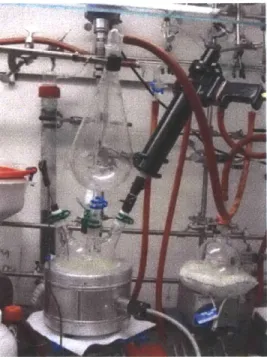
1-3. Absorption spectra of PbS QDs with a series of particle diameters. The first exitonic absorption peak of PbS QDs can be tuned readily from 600 to 2200 nm. ... 30 2-1. A photograph of colloidal QD synthesis setup, including a Schlenk line, a three-neck flask, a
condenser, a stiffer, a temperature controlling system, an injection gun, and a mechanical rotary pump (not shown in the picture). The black injection gun shown in this picture is used for large-scale (gram-scale) synthesis, while for a conventional small-scale synthesis (100 milligram-scale) synthesis, a syringe is used ... 36
2-2. Cartoon depicting the precursor concentration evolution along different stages of colloidal QD nucleation and growth under the framework of LaMer colloid growth model...36
2-3. A Scanning electron microscopy image of a treated QD film. Cracks are usually developed in thick QD film after post-deposition treatment. Cracks are usually developed in thick QD film after post-deposition treatm ent ... 39 2-4. Energy band diagram of a pn homojunction at thermal equilibrium. ... 43
2-5. Energy band diagrams of Schottky junctions formed between (a) a metal and a p-type
semiconductor and (b) a metal and an n-type semiconductor at thermal equilibrium. ... 44 2-6. A schematic diagram showing the mechanisms by which photons are converted to free
excitons, bound electron-hole pairs. (b) Excitons diffuse around in the material before radiative or non-radiative recombination. (c) When excitons reach the interface between a donor and an acceptor, charge transfer can occur. (d) Charges are spatially separated, transported, and extracted at the electrodes. HOMO and LUMO is the abbreviation of highest occupied molecular orbital and lowest unoccupied molecular orbital, respectively. 46
2-7. Ideal current-voltage characteristics of a solar cell in the dark (black curve) and under
AMi.5G illumination (red curve). An ideal solar cell I-V curve in the dark should exhibit
strong rectification...48
2-8. An equivalent circuit diagram of the solar cell comprising a current source (IL), a diode (Id),
a shunt resistor (Rsh), and a series resistor (R,). A load resistor (RL, not a part of the solar cell)
is shown in the diagram to represent the external load. ... 48 3-1. Schematic of idealized MPTMS monolayer formation on hydroxylated oxide substrate
surface with the presence of a physically-absorbed water layer...58
3-2. A photograph of the multi-vessel dip coater used to deposit high-quality PbS QD film in this
th esis...5 9
3-3. Porous and rough film grown by a homogeneous reaction. ... 61
3-4. A photograph of the custom-built Teflon substrate holder. ... 62
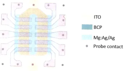
3-5. Schematic illustration of overlaid patterned ITO, BCP, and Mg:Ag/Ag electrodes. The
overlap between ITO and metal electrodes defines the ten devices with an individual active area of 1.24 mm2 on a half-inch glass substrate. The same pattern was also employed for
PbS QD/CdS bilayer heterojunction devices. The pattern was designed by Dr. Alexi Arango. ... ... 6 5
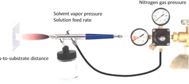
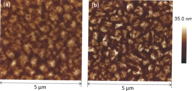
4-1. A schematic representation of a spray coating setup composed of a handheld airbrush, a gas regulator, and a nitrogen cylinder. Relevant processing parameters are also shown...70 4-2. Optical micrographs of PbS QD film deposited via (a) spin coating, (b) dip coating, and (c) spray coating . ... 7 1 4-3. AFM images of PbS QD film deposited via (a) spin coating and (b) dip coating...71
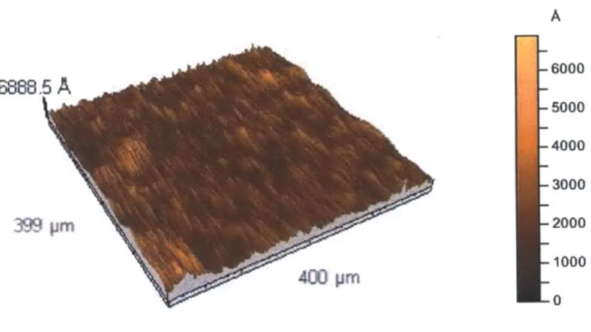
4-4. A three-dimensional profilometry image of spray-coated PbS QD film. ... 72 4-5. J-V characteristics of PbS QD Schottky devices under simulated AMI.5G illumination. PbS
QD film in these devices was deposited via (a) spin coating, (b) dip coating, and (c) spray co ating . ... 72
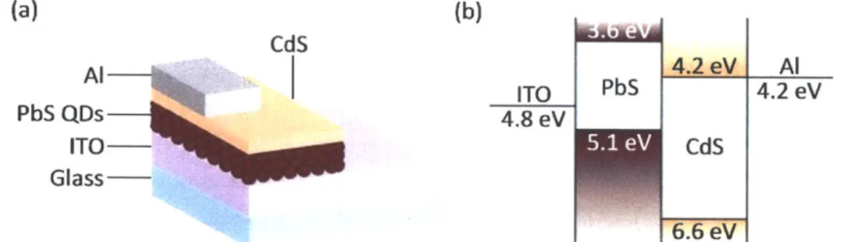
5-1. (a) Schematic of the PbS QD/CdS heterojunction device fabricated in this study. (b) Energy band diagram showing band edges of isolated 1.5eV PbS QDs and CdS along with electrode w ork functions...76
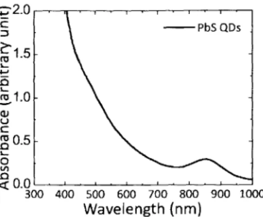
5-2. Absorbance spectrum of PbS QDs in solution used in this work. ... 77
5-3. SEM im age of the CdS thin film on glass. ... 78 5-4. Current-voltage characteristics of PbS QD and CdS thin films. The electrical conductivities
of PbS QDs and CdS were measured using a planar interdigitated configuration. For PbS QDs, the channel length is 6 ptm, the channel width is 1.95 cm, and the film thickness is 100 nm. For CdS, the channel length is 120 ptm, the channel width is 0.75 cm, and the film thickness is 120 nm. Consequently, the conductivities of PbS QDs and CdS are -2 x 10⁻⁸ and ~1 x 10⁻³ S/cm , respectively... 78
5-5. (a) Cross-sectional SEM image of the device. Platinum was deposited on top of the device
before focused ion beam milling to protect the underlying layers. (b) XPS depth profile of a
PbS QD/CdS device without Al electrodes. ... 79
5-6. J-V characteristics of nine PbS QD/CdS heterojunction devices fabricated on the same
substrate and measured under simulated AMi.5G solar illumination. The scattered J-V characteristics manifest the device irreproducibility...80
5-7. A representative top-view optical micrograph of a finished PbS QD/CdS device. Multiple
pinholes can be identified in the image. ... 80
5-8. (a) A representative top-view optical micrograph of finished PbS QD Schottky devices. No
pinhole is identified in this image. (b) J-V characteristics of nine PbS QD Schottky devices fabricated on the same substrate and measured under simulated AMI.5G solar illumination show good reproducibility. ... 81
5-9. Representative optical micrographs of (a) as-deposited PbS QD film, (b) PbS QD film with
a CdS overlayer and with no pinhole, and (c) PbS QD film with a CdS overlayer and with a pinhole. The pervasive submicron dark spots in (b) and (c) are the CdS crystallites which were initially formed in the bulk of the chemical bath solution and subsequently adsorbed and em bedded in CdS film ... 82
5-10. An optical micrograph of an ITO-coated glass substrate cleaned with the procedure
described in Chapter 3 still shows dust particles/contaminants (highlighted with the red circles) adsorbed on the surface ... 82
5-11. Optical micrographs of ITO-coated glass substrates (a) before and (b) after MPTMS
5-12. An optical micrograph of PbS QD film deposited from a solution of poor colloidal stability. Multiple particle defects can be identified in the image... 84 5-13. Photographs of centrifuged PbS QD solution added with (a) excess and (b) reduced amount of ethanol. Complete purification process should be referred to Chapter 3. The supernatant in the solution with excess amount of ethanol is much clearer than that with reduced amount of ethanol, suggesting that most of the QDs was precipitated out during centrifugation in the solution w ith excess amount of ethanol... 84 5-14. Optical micrographs of the PbS QD/CdS devices fabricated (a) without and (b) with additional measures to prevent pinhole formation. The red circles in (a) highlight the particle defects/pinholes. The blurred black spots in both images were the residual of the QD film on the back side of the substrates. During a dip-coating process, both sides of the substrates were coated, and the film on the back side was wiped off before the measurement. Therefore, these blurred spots are not in the device and can be ignored...85
5-15. J-V characteristics of nine PbS QD/CdS heterojunction devices fabricated with the
newly-implemented experimental methods on the same substrate and measured under sim ulated A M 1.5G solar illum ination... 85
5-16. J-V characteristics of typical PbS QD Schottky (red) and PbS QD/CdS heterojunction (blue) devices measured in the dark and under AM1.5G simulated solar illumination...86 5-17. J-V characteristics of an inverted CdS/PbS QD heterojunction solar cell measured in the
dark and under AMl.5G simulated solar illumination. To verify the origin of the device rectifying behavior, symmetric top and bottom ITO contacts were employed. Due to some spikes of chemical-bath-deposited CdS thin films, a thick (310 nm) PbS QD layer was used
in this inverted device to avoid shorting, which may result in a worse photovoltaic
perform ance than a norm al device. ... 87
5-18. (a) J-V characteristics of representative PbS QD/CdS heterojunction solar cells with varying PbS QD layer thicknesses. (b) Performance characteristics of the above devices. The error bars are evaluated from the standard deviation of 18 devices fabricated with the same condition for each thickness of the PbS QD film...89
5-19. Complex refractive indices of PbS QDs and CdS. ... 90
5-20. AFM surface images of (a) the PbS QD thin film and (b) the CdS thin film...91
5-21. Diffuse reflectance spectrum of a full PbS QD/CdS device (without Al electrode)...91
5-22. Measured EQE (red curves) and modeled active-layer absorption spectra (black curves) of PbS QD/CdS devices with varying PbS QD thicknesses: (a) 40 nm, (b) 100 nm, (c) 160 nm, (d) 220 nm , and (e) 280 nm . ... 89
5-23. Modeled photon absorption rate (1/sec-cm 3) for PbS QD/CdS heterojunction devices with varying PbS QD thicknesses: (a) 40 nm, (b) 100 nm, (c) 160 nm, (d) 220 nm, and (e) 280 nm. The x- axis (distance) is measured from the ITO surface where light is incident. The horizontal stripes seen in the simulation plots result from the use of AM1.5G solar spectrum as a light source for the calculated absorption/generation rate. There are multiple dips in the solar spectrum due to light absorption by 03, 02, H20, and CO2... . . . .. . . . 94
5-24. The modeled total generation rates in PbS QD layers of different thicknesses (offset for clarity)...9 5 5-25. The integrated generation rate (1/sec-cm2) as a function of the distance from the PbS QD/CdS interface for the above PbS QD thicknesses...95
5-26. Jsc integrated from the modeled (black curve, assuming 100% IQE) and measured (red
squares) EQ E spectra... 96
5-27. Measured (black square) and modeled (red circle for the lower bounds; blue triangle for the
upper bounds) device capacitance at zero-bias as a function of PbS QD thicknesses. The lower bounds were calculated, assuming that both the PbS QD and CdS layer are fully-depleted; while the upper bounds were calculated, assuming that only the PbS QD layer is fully-depleted and none of CdS layer is depleted. ... 97
5-28. Modeled short-circuit current density of the PbS QD/CdS devices with various CdS layer
thicknesses. The thickness of PbS QD layer for this modeling is fixed at 170 nm, which is effective carrier extraction range estimated in the previous sections of this thesis. ... 99
5-29. Simulated loptical electric field12 as a function of wavelength and position for various CdS thicknesses: (a) 0 nm, (b) 50 nm, (c) 180 nm, (d) 280 nm, and (e) 400 nm. The thickness of
PbS Q D layer is fixed at 170 nm ... 100 6-1. (a) The schematic device architecture and (b) the corresponding flat-band diagram...107 6-2. TEM images of (a) P3HT nanofibers and (b) CdS QDs. ... 108 6-3. UV-VIS absorbance spectra of (a) amorphous P3HT, P3HT nanofribers, and (b) CdS QDs. ... ... 10 8
6-4. TEM images of P3HT nanofiber/CdS QD film synthesized (a) without self-assembly (random-mix process) and (b) using a solvent-assisted self-assembly process. The inset images show schematic representations of each; the random-mix and self-assembly method is used to control the interface between CdS QDs (yellow spheres) and P3HT nanofibers (purp le lin es). ... 109
6-5. (a) An UV-VIS absorbance spectrum of self-assembled P3HT nanofiber/CdS QD film. (b) Solution PL spectra of the random-mixed and self-assembled P3HT nanofiber/CdS QD sam p les...1 10 6-6. XPS spectra of high resolution S2p in (a) random-mixed and (b) self-assembled P3HT
nanofiber/CdS Q D film . ... I 1
6-7. Time-resolved photoluminescence spectra of the random-mixed and self-assembled P3HT
nanofiber/CdS QD film. The film was excited by a pulsed diode laser (PicoQuant) at 414 nm, 2.5 MHz. Emission from the film was collected by an avalanche photodiode (PicoQuant) with a 460nm band-pass filter. Photoluminescence decay of the sample was measured with a time-correlated single photon counting module (PicoQuant)...111
6-8. Tapping mode AFM images of P3HT nanofiber/CdS QD thin film (a) before and (b) after EDT ligand exchange. (c) TEM image of curved P3HT NWs after the ligand exchange. . 112 6-9. Charge carrier recombination rate constants krec of pristine and EDT-treated devices
determined by transient open circuit voltage decay measurements at different illumination lev els... 1 13 6-10. (a) J-V characteristics of an electron only P3HT nanofiber/CdS QD device before and after
EDT treatment. (b) J-V characteristics of a hole only P3HT nanofiber/CdS QD device
before and after EDT treatment. The effect of EDT treatment and P3HT nanofiber curving on the transport properties of P3HT nanofiber/CdS QD film was demonstrated by the DC
J-V characteristics of the electron-only and hole-only devices. The electron-only device
consisted of Ag:self-assembled monolayer (SAM), P3HT nanofiber/CdS QD, and Mg:Ag
layers. The Ag:SAM layer blocks the hole injection [Error! Reference source not found.]. The
untreated device. The hole only device consisted of ITO, PEDOT:PSS, P3HT nanofiber/CdS QD, and Au layers, where the Au layer prevents electron injection. The treated device showed a decrease in current density. This result suggests that the EDT treatm ent reduces the hole transport...114 6-11. (a) Cross-sectional TEM image of P3HT nanofiber/CdS QD hybrid solar cells. (b) Energy
dispersive X-ray spectroscopy elemental mapping (Red color: Cd; Green color: In; and Blue: A g) of the im age show n in (a). ... 115
6-12. Cross-sectional TEM EDS mapping image of the
ITO/PEDOT:PSS/P3HT:CdS/BCP/Mg:Ag hybrid solar cell device. (a)-(d): The Mg, Cd, S, and In elem ent m apping im ages... 115
6-13. J-V characteristics of random-mixed (blue) and self-assembled (red) P3HT nanofiber/CdS Q D so lar cells...116
6-14. (a) J-V characteristics of pristine (blue) and EDT-treated (green) P3HT nanofiber/CdS QD solar cells. (b) The photovoltaic performance summary (Jsc and Voc) of the EDT-treated and self-assembled devices as a function of the CdS weight concentration...117
Chapter 1
Motivation
1.1 Solar Photovoltaic Background
Since the twentieth century, the living standard of most of the world population has increased in a significant and unprecedented way. However, at the same time, human activity has also casted a huge impact on the earth. Atmospheric carbon dioxide concentration and global surface temperature have risen since 1960 [1, 2], and evidence suggests that the global warming is a result of a rise in greenhouse gas emission caused by human activity [3]. Such change could be unsustainable or even catastrophic, if it is continued in the current fashion. Sustainable development, the development that meets the needs for economy and society without compromising the environment, is therefore one of the great challenges of the twenty-first century.
Global greenhouse gas emissions by sector from 1990 to 2005, measured in carbon dioxide equivalents, shows that the energy sector accounts for two thirds of total anthropogenic carbon dioxide emissions [4]. As a result, in order to decrease global greenhouse gas emissions, people cannot ignore the major contribution from the energy sector, including both energy production and consumption. In addition, although hydraulic-fracturing technologies have recently opened up considerable oil and gas resources, these reserves could last for only about sixty years (they may be extended by new technologies and unconventional deposits) at current consumption rates. Coal reserves will last for at least a century at current rates of consumption [5]. Nevertheless, none of these energy resources are renewable and will be exhausted in the foreseeable future. To
summary, energy plays an important role for sustainable development. We need not only reliable and affordable energy sources to continue economical and social development but also clean energy sources to mitigate the adverse effects produced during energy production and consumption on the environment.
Among various energy sources, solar energy is particularly abundant [6], and solar photovoltaics is relatively clean compared to coal-fired and natural gas power plants regarding greenhouse gas emission [7]. For the reason given above, solar photovoltaics has been growing rapidly in this past decade [8]. The global cumulative installed solar photovoltaic capacity has surpassed 100 GW in 2012, achieving just over 101 GW [9]. However, photovoltaics still enjoys marginal portions of the overall power generation. In 2010, solar photovoltaics accounted for only 0.06% of total energy consumption [8].
To accelerate the deployment of solar photovoltaics, their cost must be reduced such that solar electricity can be as cheap as the electricity generated from conventional sources such as fossil and nuclear fuels. Table 1-1 lists solar electricity price in US cents per kilowatt-hour reported in 2012 for various installation scales and climate conditions. Even the lowest price
(15.15 cents/kWh) of solar electricity generated in the industrial scale and sunny climate
condition is still well above that (~10 cents/kWh) of conventional electricity in most of the states in the United States in 2012 [11]. The cost of solar electricity can be divided into a number of components, including photovoltaic modules, electrical and structural balance of systems, inverters, labors, and other soft costs. As of 2013, photovoltaic modules still account for the largest portion (32%) of the solar electricity cost [12]. It is thus critical to cost down photovoltaic modules to decrease overall solar electricity cost.
ResdenialSunny 28.91 Residential
Installed System Cloudy 63.60
Commercial Sunny 19.42
Installed System Cloudy
42.73
Industrial Sunny 15.15
Installed System Cloudy 33.32
Table 1-1. Price of solar electricity in US cents per kilowatt-hour reported in 2012 for various installation scales and climate conditions [10]. The residential price is calculated based upon a standard 2 kilowatt peak system; the commercial price, a 50 kilowatt peak system; the industrial price, 500 kilowatt peak system.
1.2 Low-Temperature Solution-Processed Colloidal Quantum Dot
Solar Cells
Low-temperature solution-processed solar cells have
the potential to decrease manufacturing cost for photovoltaic modules. These solar cells can be built on lightweight and flexible substrates and are compatible with roll-to-roll manufacturing process such as printing. In addition, there is no vacuum process required to manufacture these solar cells. These characteristics give rise to not only low manufacturing cost but also high manufacturing throughput and short energy-payback time. Because these solar cells can be built on lightweight
and flexible substrates, the transportation and installation cost for these photovoltaic panels will be low as well.
Organic semiconductors and colloidal quantum dots are the two main material systems that can be incorporated into low-temperature solution-processed solar cells. Colloidal quantum dots are particularly interesting for photovoltaic applications because of their spectral tunability and will be the focus of this thesis.
Colloidal quantum dots (QDs) are chemically synthesized semiconductor nanocrystals coated with organic ligands (Figure 1-1) which passivate the surface of nanocrystals and provide solubility to nanocrystals in various organic solvents. The particle size of QDs can be well controlled via synthetic conditions which will be detailed in Chapter 2. When the particle size is smaller than the exciton Bohr radius [13] of the constituent semiconductor, the allowed energy levels for excitons (or electrons and holes) become quantized such that the band gap energy of the semiconductor changes with the particle size, which is termed "quantum confinement effect." The relationship between the band gap energy and particle size can be simplified and understood with a particle in a spherical box quantum mechanical model (Eg l I/d 2, Eg = band gap energy,
and d = particle diameter) as illustrated in Figure 1-2. As a consequence, the band gap energy of QDs can be tuned by controlling their particle size.
Inorganic semiconductor core
Organic ligand shell
Figure 1-1. Schematic of a colloidal quantum dot with inorganic semiconductor core and organic ligand shell.
Particle in a box
Conduction Band
Valence Band Decreasing particle sizes
Increasing band gaps
Figure 1-2. The effect of quantum confinement on the energy levels of electrons (solid circle) and holes (open circle) in semiconductor nanoparticles.
Table 1-2 summarizes theoretical power conversion efficiency (Shockley-Queisser limit [14,
15]) of single- and multijunction solar cells and the corresponding optimal band gap energy for
the constituent junctions. Multijunction solar cells, consisting of multiple semiconductors of different band gap energy, extract solar energy more efficiently and promise for higher efficiency. For example, power conversion efficiency increases from 31% to 49% when triple junctions, instead of single junction, are employed. However, since multiple semiconductors are involved in the multijunction solar cells, considerable effort has to be exerted to optimize the properties of constituent materials, which significantly increases the manufacturing complexity and cost of these cells. Band gap tunability of QDs offers the opportunity to realize multijunction solar cells
with single semiconductor material, providing the potential to offset the manufacturing disadvantages derived from multijunction devices. As shown in Figure 1-3, PbS QDs covers all the optimal band gap energies for triple-junction solar cells.
Number of 23 junctions 1750 nm 1320 nm 170n Band gap 1100 nm 760nm 1070 nm 760 nm 680 nm Efficiency 31% 44% 49%
Table 1-2. Theoretical power conversion efficiency of single- and multijunction solar cells and the corresponding optimal band gap energies for the constituent junctions. Band gap energies are expressed with equivalent photon wavelength.
7 6 5 UJ4 C 0i2 0-400 800 1200 1600 2000 Wavelength (nm)
Figure 1-3. Absorption spectra of PbS QDs with a series of particle diameters. The first excitonic absorption peak of PbS QDs can be tuned readily from 600 to 2200 nm [16-18]. On the other hand, the band gap of bulk PbS is 0.41 eV, which is approximately 2958 mu.
It has to be noted that although the band gap of Cu(In,Ga)Se2, an extensive studied semiconductor for a thin film solar cell, can be adjusted by substitution of Ga for In, its band gap changes from 1.04 to 1.67 eV (or 1195 to 744 nm) [19] and does not cover most of the band gaps
calculated for multijunction solar cells (Table 1-2).
1.3 Thesis Outline
This thesis focuses on the electron-hole separation junction (or interface), one of the key elements in solar cells. Specifically, it tackles inorganic-inorganic bilayer heterojunctions and inorganic-organic bulk heterojunctions; both of which involve QDs.
Chapter 2 first gives an overview of QD synthesis then reviews electrical properties (carrier mobility, carrier type, and carrier concentration) of QDs and solar cell device physics, including photovoltaic mechanisms in both inorganic and organic solar cells, and current-voltage characteristics of solar cells. The chapter provides the chemistry and physics background for colloidal QD-based solar cells.
Chapter 3 elaborates the experimental procedures for the material synthesis and the fabrication and characterization of PbS QD/CdS bilayer heterojunction devices and poly(3-hexylthiophene-2,5-diyl) nanofiber/CdS QD bulk heterojunction devices.
Chapter 4 presents PbS QD Schottky devices fabricated by spin coating, dip coating, and spray coating. Comparison of film morphology and device performance in the spin-, dip, and spray-coated devices is reported. This chapter paves the way for the fabrication of PbS QD photovoltaic devices with high yield and satisfying reproducibility.
Chapter 5 describes the realization, optimization and characterization of PbS QD/CdS bilayer heterojunction devices, the first low-temperature solution-processed pn heterojunction devices employing PbS QDs. Through a combination of characterization techniques, fundamental material and device parameters are reported.
poly(3-hexylthiophene-2,5-diyl) nanofiber/CdS QD bulk heterojunction solar cells through the modification of the interfacial interaction between organic electron donors and inorganic electron acceptors.
Chapter 7 summarizes the findings made from this thesis work and briefs the future work that can be done to further improve the efficiency of QD-based photovoltaic devices.
1.4 Reference
1 Source: Met Office Hadley Centre; NOAA; Scripps Institute of Oceanography; Sydney Levitus et al, GRL
2 Climate change: The measure of global warming, The Economist, 2013
3 Etheridge, D. M.; Steele, L. P.; Langenfelds, R. L.; Francey, R. J.; Barnola, J.-M. & Morgan, V. I., Natural and anthropogenic changes in atmospheric C02 over the last 1000 years from air in Antarctic ice and firn, Journal of Geophysical Research: Atmospheres, 1996, 101,
4115-4128
4 Climate Analysis Indicators Tool, World Resources Institute, 2009
5 Jeff Tollefson & Richard Monastersky, Nature, 2012, 491, 654-655
6 Graetzel, M.; Janssen, R. A. J.; Mitzi, D. B. & Sargent, E. H., Materials interface engineering for solution-processed photovoltaics, Nature, 2012, 488, 304-312
7 U.S. Department of Energy, Report on the First Quadrennial Technology Review, 2011 8 REN2 1, Renewables Global Status Report, 2012
9 European Photovoltaic Industry Association, 2013. 10 Solarbuzz Retail Pricing Environment, 2012 11 U.S. Energy Information Administration, 2012
12 GTM Research, Solvida Energy Group, Inc., 2012
13 Excitons are bound electron-hole pairs. The exciton Bohr radius is the avarage distance between the electron and hole of an exciton in its ground state.
14 Shockley, W. & Queisser, H. J.Detailed Balance Limit of Efficiency of p-n Junction Solar Cells, Journal of Applied Physics, 1961, 32, 510-519
15 Sargent, E. H., Infrared photovoltaics made by solution processing, Nat Photon, 2009, 3, 325-33
16 Hines, M. & Scholes, G., Colloidal PbS Nanocrystals with Size-Tunable Near-Infrared Emission: Observation of Post-Synthesis Self-Narrowing of the Particle Size Distribution, Adv. Mater., 2003, 15, 1844-1849
17 Liu, T.-Y.; Li, M.; Ouyang, J.; Zaman, M. B.; Wang, R.; Wu, X.; Yeh, C.-S.; Lin,
Q.;
Yang, B. & Yu, K., Non-Injection and Low-Temperature Approach to Colloidal Photoluminescent PbS Nanocrystals with Narrow Bandwidth, The Journal of Physical Chemistry C, 2009, 113, 2301-230818 Moreels, I.; Justo, Y.; De Geyter, B.; Haustraete, K.; Martins, J. C. & Hens, Z., Size-Tunable, Bright, and Stable PbS Quantum Dots: A Surface Chemistry Study, ACS Nano, 2011, 5, 2004-2012
19 Wei, S.-H.; Zhang, S. B. & Zunger, A., Effects of Ga addition to CuInSe2 on its electronic, structural, and defect properties, Applied Physics Letters, 1998, 72, 3199-3201
Chapter 2
Basics of Colloidal Quantum Dot Solar Cells
This chapter is to provide introductory and theoretical background for colloidal QD solar cells, including colloidal QD synthesis, optical and electrical properties of QDs and methods to tune these properties, and solar cell device physics and electrical characteristics.
2.1 Colloidal Quantum Dot Synthesis
The investigation of colloidal quantum dots began in early 1980s, when CdS nanocrystals with broad size distribution were precipitated and grown via Ostwald ripening in aqueous solution [1]. A breakthrough in synthesizing monodisperse colloidal QDs was made by Chris Murray, David Norris, and Moungi Bawendi in 1993, when hot injection method [2] was first introduced. Since then, there have been numerous studies attempting to improve size distribution and optical property of colloidal QDs and also change the morphology, composition, and chemistry of colloidal QDs. However, hot injection method remains the mainstream colloidal QD synthesis protocol because of the narrow size distribution it can provide. Therefore, colloidal QDs in this thesis are synthesized via hot injection method.
Detailed description of synthesis procedure for colloidal QDs of different compositions will be provided later in the corresponding chapters. Here, a generalized colloidal QD synthesis is presented. Colloidal QD synthesis is performed with a Schlenk line which provides air- and moisture-free environment. Figure 2-1 shows the photograph of the setup used for colloidal QD synthesis. One precursor compound is first dissolved in a heated high-boiling point solvent contained and degassed in a three-neck flask. The precursor solution is further heated to the reaction temperature. Then, another degassed precursor solution is swiftly injected to the flask,
which raises the precursor concentration above the nucleation threshold and leads to a nucleation burst. Figure 2-2 illustrates precursor concentration as the reaction evolves according to LaMer colloid growth model [3]. Rapid injection ensures that most of nuclei formed at the same time. In an ideal case, the lowering of precursor concentration due to the nucleation event and the reducing of overall solution temperature due to the addition of a room-temperature precursor solution terminates nucleus formation. Precursors are then consumed by the nanocrystal growth. The quenching of nucleus formation prior to or at the early stage of nanocrystal growth is a key for narrow particle size distribution achieved with hot injection colloidal QD synthesis because it allows all nanocrystals to grow at the same time. Eventually, the reaction will reach equilibrium between material in nanocrystals and precursor monomers, and the size distribution will start to increase because big particles grow at the expense of small particles' shrinkage known as Ostwald ripening.
Particle size can be controlled via various synthesis conditions, such as precursor reactivity, coordinating/non-coordinating solvent ratio, growth temperature, and growth period. When more reactive precursor is used, more nuclei are formed, resulting in smaller particle size and larger size distribution [4]. Coordinating solvent promotes precursor consumption by nanocrystal growth, which leads to larger particle size [5]. Higher growth temperature and longer growth period also increase particle size.
Figure 2-1. A photograph of colloidal QD synthesis setup, including a Schlenk line, a three-neck flask, a condenser, a stirrer, a temperature controlling system, an injection gun, and a mechanical rotary pump (not shown in the picture). The black injection gun shown in this picture is used for large-scale (gram-scale) synthesis, while for a conventional small-scale synthesis (100 milligram-scale) synthesis, a syringe is used.
C 0 C Z U .0 Nucleation threshold o C 4. = U ~ (U + Ostwald ripening Time
Figure 2-2. Cartoon depicting the precursor concentration evolution along different stages of colloidal QD nucleation and growth under the framework of LaMer colloid growth model.
2.2
Electrical Properties of Colloidal Quantum Dots
After synthesis, colloidal QDs are capped with long-chain organic ligands, such as oleic acid, oleylamine, trioctylphosphine, and trioctylphosphine oxide, which provide solubility to QDs in a range of organic solvents. The capping ligands also play an important role in the electrical properties of colloidal QDs, such as carrier mobility, carrier type and concentration, and carrier traps.
2.2.1 Carrier Mobility
In a thin film composed of colloidal QDs, carriers are transported via either tunneling or hopping mechanisms which are largely affected by the distances between adjacent QDs. Therefore, a lot of effort has been made to shrink the inter-QD distances to improve carrier mobility. This is generally achieved via solution- or solid-phase chemical treatments by which long-chain organic ligands are replaced by short organic or inorganic ligands. Although carrier mobility can also be increased by a high-temperature annealing process which sinters QD thin film [6], the quantum confinement effect is lost and thus is not within the focus of this thesis.
Solution-phase chemical treatment here is a pre-deposition ligand exchange process occuring in a QD solution and requires the preservation of colloidal stability of QDs after ligand exchange for the following thin film deposition with small roughness. Common organic molecules for solution-phase ligand exchange are pyridine [7] and n-butylamine [8]. Recently, Dmitri Talapin's group developed molecular metal chalcogenide complex ligands and achieved electron mobility as high as 16 cm2/Vs for CdSe colloidal QDs with In
2Se2 ligands [9]. Cherie
Kagan's group also demonstrated thiocyanate-capped CdSe QD thin film with high electron mobility of 1.5 ± 0.7 cm2/Vs [10]. Both of these values are acquired by field effect transistor
measurement and are considered very high for non-sintered colloidal QD thin film. Although the physical size of the ligands used in these two cases are tiny, these ligands charge QD surfaces and provide electrostatic repulsion between QDs, which prevents aggregation and offers
solubility in polar solvents.
Solid-phase chemical treatment, on the contrary, is a post-deposition ligand exchange process carried out after QD thin film is deposited. Small ligands, such as 1,2-ethanedithiol [11], 1,4-benzenedithiol [12], 3-mercaptopropionic acid [13], and hydrazine [14], used in this process drastically shorten inter-QD distances and insolubilize QDs. Untreated oleic acid capped-PbS QDs with hole field-effect mobility of 3 x 10- cm2/Vs is reported [15]. After treated with 1,2-ethanedithiol, 1,4-benzenedithiol, and 3-mercaptopropionic acid, hole field-effect mobility is
increased to 1.7 x 10⁻³ 3.8 x 10-, and 2.7 x 1 0-3 cm2/Vs, respectively [16]. In addition, Yao Liu
et al. have also shown that electron and hole field-effect mobility decrease exponentially with increasing ligand length [17]. Recently, Edward Sargent's group has also demonstrated that with halide treatments, such as cetyltrimethylammonium bromide, the electron field-effect mobility of
PbS QDs can be improved to 4.4 x 102 cm2/Vs [18]. Because of the large volume shrinkage, cracks usually form in the treated QD film as shown in Figure 2-3. Therefore, layer-by-layer coating techniques are employed to fill the cracks generated in the underlying layers to prevent shorts.
Figure 2-3. A Scanning electron microscopy image of a treated QD film. Cracks are usually developed in thick QD film after post-deposition treatment.
In summary, carrier mobility in QD film is strongly correlated with the capping ligands: the shorter the ligand, the higher the mobility. Various solution- and solid-phase chemical treatments are implemented to replace bulky native ligands with short ligands, providing a pathway toward solution-processed high-performance electronic and optoelectronic devices.
2.2.2 Carrier Type and Density
Carrier type and density are important factors for the operation of solar cells as will be described later in this chatper. It has been reported in several QD material systems that carrier type and density can be controlled via chemical treatment and are also sensitive to the environment to which QDs exposed.
Conduction of PbSe QDs can be switched from p- to n-type by hydrazine post-deposition treatment and reversed to p-type as the hydrazine desorbed [14]. By increasing the doping level, silver can be changed from n- to p-type dopants for CdSe QDs [19]. N-type doping of CdSe QDs can also be realized by thermal diffusion of indium [9], and electron transfer from sodium
biphenyl [20]. Metal chalcogenide complexes allow switching of CdTe QD conduction from p-type to ambipolar to n-type [21]. Pre-deposition incorporation of cadmium switches conduction of InAs QDs from n- to p-type [22]. Chemical treatments, including organic and halide ligands, are employed to tailor doping type and concentration of PbS QDs [23, 24, 25]. Oxidation is found to increase p-type doping of PbS QDs [15]. In addition, carrier type and density in PbSe QDs are shown to be connected to QD's stoichiometry: Pb-rich QDs are n-type; Se-rich, p-type [26].
2.3 Solar Cell Device Physics
A solar cell is a semiconductor diode which directly converts sun light into electricity. In a conventional inorganic solar cell, this conversion process primarily consists of photon absorption (carrier generation) and carrier separation. While in an excitonic solar cell, such as an organic solar cell [27], very similar but not exactly identical processes are involved, namely photon absorption (exciton generation), exciton diffusion, charge transfer, charge separation, carrier transport and carrier extraction [28]. Since this thesis work involves both inorganic and organic solar cells, in the following sections I will first describe the details of these processes in conventional inorganic solar cells, followed by the explanation of similar conversion process in organic solar cells.
2.3.1 Photovoltaic Processes in Inorganic Solar Cells Photon Absorption and Carrier Generation:
When light shines on a solar cell, photons, if not reflected from the solar cell, with energy equal to or greater than the band gap of semiconductors can be absorbed. Such photon absorption
event excites electrons from valence bands to conduction bands and generates free carriers (electrons and holes). However, not all the photons with energy equal to or greater than the band gap of semiconductors are absorbed. In materials with low absorption coefficient or small thickness, photons can transmit without being absorbed, even though their energy is sufficient to excite electron from valence bands to conduction bands. Therefore, reflection and transmission are two of the loss mechanisms that need to be eliminated or minimized to achieve high photocurrent density and high device performance.
The number of free carriers generated by photon absorption is limited by the flux of photons with enough energy to excite electrons from valence bands to conduction bands. The smaller the band gap of semiconductors, the more free carriers can be generated by photon absorption. However, because carriers generated by high-energy photons (with energy greater than the band gap of semiconductors) relax rapidly to the band edge of semiconductors and also because of energy conservation, the usable energy is smaller when semiconductors of smaller band gaps are employed. Due to this trade-off, to realize high device efficiency, there is an optimal band gap for the semiconductor used in a solar cell as mentioned in chapter one.
Although there are approaches proposed to exploit or better use photons with energy smaller or greater than the band gap of semiconductors, such as an intermediate-band solar cell [29], a multiple exciton generation solar cell [30], and a hot carrier solar cell [31], these types of device are still in their very early stage of research and rather immature and thus are beyond the scope of this thesis.
Carrier Separation:
and drift processes are minority carrier diffusion length and depletion width. For the carriers generated outside of the depletion region, they need to diffuse to the depletion region, but the distance they can diffuse before annihilated via recombination is limited by the minority carrier diffusion length. For the carriers generated in or successfully diffusing into the depletion region, they can be swept by the built-in electric field to the corresponding electrodes and contribute to electric current. Built-in electric field is typically formed in a semiconductor-semiconductor pn junction or a metal-semiconductor Schottky junction which forms the basis of a solar cell and is
elaborated in the following paragraphs.
When p-type and n-type semiconductors are joined together, due to the electron and hole concentration gradient across the p-type and n-type semiconductor junction, holes in the p-type semiconductor diffuse to the n-type semiconductor, and electrons in the n-type semiconductor diffuse to the p-type semiconductor to establish chemical potential equilibrium. The diffusion of free carriers leaves behind uncompensated positively charged donor atoms in the n-type semiconductor and negatively charged acceptor atoms in the p-type semiconductor. The charged atoms created the so-called built-in electric field (or built-in potential, Vbi, or energy band bending) which sweeps away free carriers in the junction region, and the junction region where
free carriers are depleted is named depletion region whose width is denoted as Wd and equal to:
=[2-cs-o (NA+ND) Vbi 21 W4/c = q2 NA+ND bi]1/2 21
where es, co, q, NA, and ND are the dielectric constant of the semiconductor, vacuum permittivity, elementary charge, acceptor concentration and donor concentration, respectively. Figure 2-4 shows the energy band diagram of a pn homojunction at thermal equilibrium. The depletion width, WP, in the p-type semiconductor and the depletion width, W,, in the n-type semiconductor are given by:
ND 1/2
WP = [Iq NA(NA +ND) Vbi (2-2)
Wn = ND (NA+ND) bi 1/2 (2-3)
It can be seen from equation 2-2 and 2-3 that the depletion region is not evenly distributed in the p-type and n-type semiconductors; instead, it spreads mostly in the less-doped side of the semiconductor (either in the p-type or n-type semiconductor). As a result, in heterojunction solar cells such as CdTe/CdS and CIGS/CdS solar cells [32, 33], it is preferred to have the absorber layer less doped than the window or buffer layer to extend most of the depletion width in the absorber layer and facilitate carrier separation.
depletion region EC electrons EC EF holes EF w W p-type n-type
Figure 2-4. Energy band diagram of a pn homojunction at thermal equilibrium.
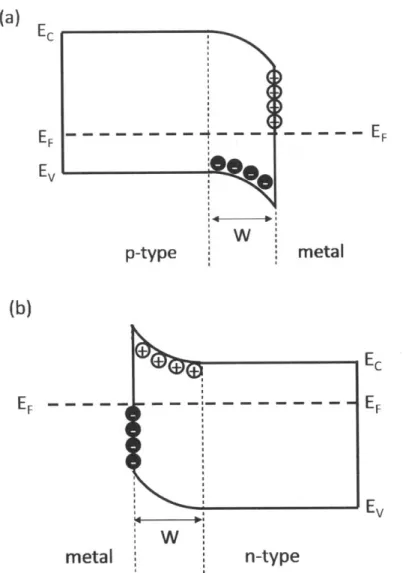
When a metal and semiconductor are brought into contact, energy band bending and depletion regions can also be established as in the case of pn semiconductor junctions. Such metal-semiconductor junction is known as a Schottky junction in which the metal can be conceived as a very heavily doped semiconductor and essentially all the depletion region resides in the semiconductor side as depicted in Figure 2-5.
(a) EF---- - - - - - - - - - EF W p-type metal
(b)
EC EF - - - - - - - - - -EF Ev W metal n-typeFigure 2-5. Energy band diagrams of Schottky junctions formed between (a) a metal and a p-type semiconductor and (b) a metal and an n-type semiconductor at thermal equilibrium.
2.3.2 Photovoltaic Processes in Organic Solar Cells
Conversion of light to electricity in an organic solar cell takes on the mechanistic steps very similar to the ones in an inorganic solar cell but with some differences due to the material properties of organic semiconductors.
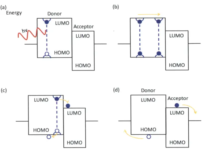
pairs immediately. In conjugated polymers, only 10% of photoexcitations with energy above the band gap directly create free charges [34]. The majority of the photoexcitations in organic semiconductors forms coulombically bound electron-hole pairs, called excitons, due to small dielectric constants and resultant large exciton binding energy (estimated to be 0.4-0.5 eV [35]) in these materials [27]. These excitons have to diffuse to dissociation sites to be broken apart into free carriers. The dissociation process can be achieved by blending two organic semiconductors of different energy levels together such that it is energetically favorable to transfer electrons from a donor material to an acceptor material and holes from an acceptor material to a donor material. Although the transferred electrons and holes (charge-transfer exitons) can still attract each other, these excitons have decreased binding energy because of increased separation between electrons and holes and thus more susceptible to dissociation under electric fields or thermal activation. The spatially separated charges then need to transport to and be extracted at an anode and cathode in order to contribute to photocurrents. The sequential photovoltaic process starting from photon absorption to carrier extraction in an organic solar cell is schematically illustrated in Figure 2-6.
(a) Energy (c) LUMO (b) Donor LUMO HOMO LUMO HOMO__ Acceptor LUMO | HOMO (d) I I I I I I Donor LUMO HOMO LUMO HOMO Acceptor LM HOMO IHOMO
Figure 2-6. A schematic diagram showing the mechanisms by which photons are converted to free carriers in an organic solar cell. (a) Photon absorption in semiconductor layers generates excitons, bound electron-hole pairs. (b) Excitons diffuse around in the material before radiative or non-radiative recombination. (c) When excitons reach the interface between a donor and an acceptor, charge transfer can occur. (d) Charges are spatially separated, transported, and extracted at the electrodes. HOMO and LUMO is the abbreviation of highest occupied molecular orbital and lowest unoccupied molecular orbital, respectively.
2.3.3 Current-Voltage Characteristics of Solar Cells
Although the photovoltaic processes involved in inorganic and organic solar cells are different, current-voltage characteristics of these devices are identical. Figure 2-7 presents ideal
current-voltage (I-V) curves of a solar cell in the dark and under AM1.5G illumination. When a forward bias is applied on a solar cell in the dark, carriers are injected across the potential barriers at a semiconductor-semiconductor or a metal-semiconductor interface such that the current flowing through the device increases exponentially with a positive bias as described in the Shockley diode equation:
SqV
Id= Io (en' - 1) (2-4)
where Id is the current flowing through the diode, 1o is the reverse saturation current, n is the ideality factor, k is the Boltzmann constant, and T is the absolute temperature. Under illumination, a photocurrent (IL) is generated and can be superimposed to the diode current, shifting the diode current downward in a current-voltage plot:
qV
I = JO (en - 1) - 1, (2-5)
Current, voltage, and thus output power is available from the device with the power conversion efficiency (PCE) defined as the ratio of maximum output power to input power and is a critical figure of merit for a solar cell. Input power is the product of device area and the incident light intensity, and the standard incident solar spectrum at the Earth's surface is AM1.5G with integrated power density equal to 100 mW/cm2. Maximum output power (Po
0 t) is the product of
optimal current (Im.) and voltage (Vm,) and can be expressed as:
Pout = Isc X Voc X F F (2-6)
where ISc is the short-circuit current, VOC is the open-circuit voltage, and FF is the fill factor. Fill factor is the ratio of the optimal current and voltage product to the short-circuit current and open-circuit voltage product, defining the "squareness" of the current-voltage curve in the fourth quadrant of a solar cell under illumination.
41-J
Voltage
Figure 2-7. Ideal current-voltage characteristics of a solar cell in the dark (black curve) and under
AM1.5G illumination (red curve). An ideal solar cell I-V curve in the dark should exhibit strong
rectification.
However, a solar cell in reality is not merely composed of an ideal diode, and thus the I-V curve can deviate appreciably from the one depicted in the Figure 2-6. To account for the non-ideality, shunt resistance (Rsh) and series resistance (R,) are included in the equivalent circuit diagram (Figure 2-8) used to describe the electrical behavior of the device. The components in the equivalent circuit diagram are expatiated in the following paragraph.
RS ld IshI
L sh V RL
-0-Figure 2-8. An equivalent circuit diagram of the solar cell comprising a current source (IL), a diode (Id), a shunt resistor (Rh), and a series resistor (R,). A load resistor (RL, not a part of the solar cell) is shown in the diagram to represent the external load.
-- AM1.5G Dark
![Table 1-1. Price of solar electricity in US cents per kilowatt-hour reported in 2012 for various installation scales and climate conditions [10]](https://thumb-eu.123doks.com/thumbv2/123doknet/14733738.573655/27.918.255.639.143.494/table-electricity-kilowatt-reported-various-installation-climate-conditions.webp)