HAL Id: lirmm-01234076
https://hal-lirmm.ccsd.cnrs.fr/lirmm-01234076
Submitted on 6 Jun 2019
HAL is a multi-disciplinary open access
archive for the deposit and dissemination of
sci-entific research documents, whether they are
pub-lished or not. The documents may come from
teaching and research institutions in France or
abroad, or from public or private research centers.
L’archive ouverte pluridisciplinaire HAL, est
destinée au dépôt et à la diffusion de documents
scientifiques de niveau recherche, publiés ou non,
émanant des établissements d’enseignement et de
recherche français ou étrangers, des laboratoires
publics ou privés.
3D DFT Challenges and Solutions
Yassine Fkih, Pascal Vivet, Marie-Lise Flottes, Bruno Rouzeyre, Giorgio Di
Natale, Juergen Schloeffel
To cite this version:
Yassine Fkih, Pascal Vivet, Marie-Lise Flottes, Bruno Rouzeyre, Giorgio Di Natale, et al.. 3D DFT
Challenges and Solutions. ISVLSI: International Symposium on Very Large Scale Integration, Jul
2015, Montpellier, France. pp.603-608, �10.1109/ISVLSI.2015.11�. �lirmm-01234076�
3D DFT Challenges And Solutions
Yassine Fkih(1,2), Pascal Vivet(1),
Marie-Lise Flottes(2),Bruno Rouzeyre(2), Giorgio Di Natale(2), Juergen Schloeffel(3)
(1) CEA-Leti, MINATEC Campus, F38054, Grenoble France (2) LIRMM, Univ Montpellier II/CNRS, Montpellier France
(3) Mentor Graphics, Hamburg, Germany
Abstract—Design-For-Test (DFT) of 3D stacked integrated
circuits based on Through Silicon Vias (TSVs) is one of the hot topics in the field of test of integrated circuits. This is due to the test access complexity of dies’ components that must be controlled/observed before and after bonding (especially for upper dies), and the high complexity of 3D systems where each die can embed hundreds of IPs. DFT of 3D circuits concerns all the components of the 3D system, including the dies and the inter-die interconnections. We address the problem of test architecture definition for both TSVs testing before bonding and cores testing before and after bonding. We present test solutions allowing to access the components under test while physical interconnects for test data propagation differ according to the stacking step. The paper also discusses core test scheduling issues.
Key words: 3D-IC, Design-For-Testability, IEEE 1687, test scheduling
I. INTRODUCTION
The stacking process of integrated circuits using TSVs (Through Silicon Vias) is a promising technology that keeps the development of the integration more than Moore’s law, where TSVs enable the tight integration of various dies in a 3D fashion. 3D stacking will allow a wide range of new applications thanks to high performance, smaller form factors, heterogeneous stacking (digital, memory, RF, MEMS), and interposers for multi-chip connection, which become similar to silicon boards. The first upcoming 3D applications are mainly the WideIO DRAM 3D memory interface for high throughput and low power memory-on-logic stacking [1].
3D Integrated Circuits (3D-ICs) present however new test challenges related to the new fabrication process. Indeed the test may have to be performed at pre-bond phase, mid-bond phase, and post-bond phase to guarantee the production quality. Pre-bond test targets the individual dies at wafer level, by testing not only classical logic (digital logic, IOs, RAM, etc.) but also non bonded TSVs. Mid-bond test targets the test of partially assembled 3D stacks, whereas post-bond test targets the final circuit. It is generally admitted that a 3D test flow [2] should involve test procedures at all stacking levels of the 3D components.
A first issue is regarding the test of new 3D elements themselves, such as TSV and µ-bumps, with associated 3D test defaults. A second test issue concerns the overall 3D Design-For-Test (DFT) architecture. It must be compatible with existing test standards, allow test in pre-, mid- and post-bond phases, and offer enhanced test scheduling within the 3D
stack. In addition, the possibility of easy test pattern retargeting from 2D (die-level) to 3D (stack-level) is definitely a plus. While test scheduling aims to optimize the test time on every stack, test pattern retargeting is of primary concern for industry to reduce test development efforts to translate test patterns from dies to stacks.
Many DFT architectures for testing 3D integrated circuits have been proposed in the past. The first papers treated pre-bond test of 3D processors using scan islands and the so-called Layer Test Controller (LTC) [3], scan chain optimization approaches [4], and other test issues like test cost optimization [5]. More recent works propose die level wrappers based either on IEEE 1500 [6] or IEEE 1149.1 [7] test standards. These test architectures have mainly three features: the use of dedicated probe pads for pre-bond testing on every stack tier, the usage of “TestElevators” [6, 7] to drive test signals up and down during post-bond test of non-bottom dies through the bottom die, and the use of a hierarchical WIR (Wrapper Instruction Register) chain to configure test paths. These features satisfy 3D circuits testing requirements in case of homogenous 3D-ICs where all dies have similar interfaces (e.g. IEEE 1149.1). A new standard IJTAG, or IEEE 1687, is currently methodology for accessing instrumentation embedded within a semiconductor device, without defining the instruments or their features themselves, it incorporates IEEE 1149.1-x and the design-for-test standard IEEE 1500. We note that proposals should be in line with the on-going 3D test working group IEEE P1838 [8].
Assuming dies from different sources, test interfaces must be define to provide compatible test access mechanisms between the different dies, facilitate exchange of test information between Design-for-Test engineers, Test CAD tools, and Test engineers, and allow implementation of various test schedules according to the test phase.
This paper discusses DFT issues for 3D-SICs from different perspectives including the pre-bond test of TSVs and the definition of the DFT architecture at system level taking into account test pattern retargeting and test scheduling flexibility challenges.
The paper also presents experiments performed from envisaged solutions. It is organized as follows: section II deals with the pre-bond test of TSVs, it highlights the challenges, presents the BIST solution we have developed for testing these vertical interconnects while they are not yet bonded, and shows its ability to distinguish faulty TSVs from fault-free
This work was funded thanks to the French national program 'programme d’Investissements d’Avenir, IRT Nanoelec' ANR-10-AIRT-05
And was conducted in the framework of the Catrene CT312
MASTER3D project and received financial support from the “Ministère du Redressement Productif”
ones on real experimental data. Section III presents the proposed 3D DFT architecture based on IEEE 1687 and details the main features that enable automatic test path configuration according to the test phase, its flexibility w.r.t. the stack under test, and its ability to provide test pattern retargeting. In Section IV, we make the link between the flexibility of our 3D DFT architecture and 3D test scheduling. Finally, section V concludes the paper.
II. PRE-BOND TEST OFTSVS
Testing TSVs at pre-bond level contributes towards production of Known Good Dies before stacking.
The testability of TSVs before bonding has been the subject of several research works which can be divided in two categories: the first category relies on fine probe heads to establish direct contacts with TSVs [9,10,11], and the second is based on indirect measurements using dedicated test pads and embedded test infrastructures [12,13,14,15,16]. Our proposed test architecture detailed in [17] belongs to this second approach.
The principle is to use ring oscillators to evaluate the electrical characteristics of TSVs (capacitance). A Built-In-Self-Test (BIST) infrastructure elaborates the measurement of the frequencies of the ring oscillators and generates signatures. Communication with the BIST logic is ensured by the mean of a JTAG interface. JTAG interf ace TSVs JTAG TAP Controller Ring Oscillators Functional logic TSVs BIST Controller Substrate
Figure 1. Pre-bond test of TSVs using ring oscillators
The ring oscillators are directly connected to the accessible end of TSVs (see Fig.1). Their frequencies depend directly on the capacitance of these vertical interconnects, and thus, a frequency variation is an image of a capacitance variation (defect) in the TSV under test. The detection of a frequency variation is done by comparing all ring oscillators in the circuit.
A. Design of the ring oscillators
The design of a ring oscillator for TSV testing depends on several parameters including the number of TSVs per ring oscillator (either a large ring oscillator charging many TSVs or a small ring oscillator charging only one TSV), and the electrical characteristics of the inverters (capacitance) used in the ring to provide oscillations. Sensitivity to PVT (Process, Voltage, and Temperature) variations is also an issue.
As detailed in [17], our test method is based on a relative frequency variation measurement, which has been shown robust against global PVT variations. The best fault detection accuracy has been obtained for only one TSV connected per
ring oscillator and inverters providing the smallest input capacitance.
B. Design of the BIST circuitry
The BIST architecture ensures the launch of the BIST procedure, the counting of the number of oscillations for each ring oscillator during a given time, the comparison between oscillator frequencies, and the generation of the final test result. In order to limit the area overhead, we chose to implement only one counter, the BIST structure thus also selects the ring oscillators to be measured one by one.
The proposed BIST supports 3 possibilities of feedback: pass/fail, diagnostic and debug. The pass/fail feature allows a quick test of the TSVs by comparing the frequencies of the ring oscillators. If the difference between the maximum and the minimum measured frequencies exceeds a user-programmable threshold, the BIST returns 0 (Fail), 1 otherwise (Fault-free). The ‘diagnostic’ option returns the total number of the failing TSVs, and the ‘debug’ option returns their positions in the chip.
The user-programmable threshold TTT (TSV Test Threshold) [17] can be set to values ranging from 5% to 50% (step=5%). Tuning the TTT parameter can be used for TSVs characterization: TTT is first set to a large value (50% of deviation) then gradually decreased until the test fail. The last TTT value for which the test passes corresponds to the dispersion of the TSV characteristics in the circuit.
C. Test chip implementation
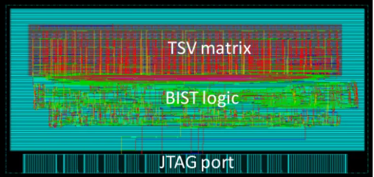
We implemented the circuit shown in Figure 1, as a test chip prototype for one channel matrix of a WideIO memory including 276 TSVs. Synthesis results using the STMicroelectronics 65nm library shows that the area of our proposed BIST architecture, including the ring oscillators, represents only 2% of the TSVs area.
TSV matrix
BIST logic
JTAG port
Figure 2. Layout of the BIST of pre-bond test of TSVs
The layout of the test chip is shown in Figure 2. The ring oscillators were placed as close as possible to the TSVs, within the TSVs matrix, in order to limit the area overhead and the impact of local (intra-chip) PVT variations on the measurement.
A simulation of the BIST procedure for 1000 TSVs shows a total test time of 2ms with a JTAG clock of 50 MHz and a BIST clock of 100 MHz.
D. Application on real technological data
TSV reliability measurements have been performed on TSV matrices from CEA-LETI with following characteristics: diameter=10µm, length=80µm (AR=1/8). The expected TSV resistance and capacitance are around 25 Ohm and 250 fF respectively.
The summary of the capacitance measurements are presented below. The plots present a histogram of the measured capacitances, and a color map at waver level shows the localization of potential TSV defects (values out of range). Measurements were done on ‘correct’ wafers and ‘incorrect’ wafers (with injected faults).
Figure 3.a Capacitance measurements of TSVs on correct wafers
Figure 3.a shows measurement results from a correct wafers, the measured mean capacitance of TSVs is around 250 fF, with a standard deviation value of 12fF, which give an overall yield of 95% in case of correct wafers.
Figure 3.b Capacitance measurements of TSVs on incorrect wafers
Figure 3.b shows measurement results corresponding to incorrect wafers, the measured mean capacitance equals to 435 fF with a standard deviation (sigma) of 58 fF and an overall yield of 78%.
As a summary, the dispersion is clearly very large, and can be observed by the mean of our proposed BIST approach based on ring oscillators. In such context the detection of faulty TSVs is done using a comparison approach called “average approach”, where the average oscillation frequency among all the TSVs is calculated by the BIST logic and the left and right limits are defined by the mean of the TTT user-programmable threshold (see fig. 4).
Figure 4. Binning strategy of the measured frequencies.
Applied in a case such the one shown in Figure 3.b where TSVs are considered as faulty if their capacitance exceeds 3 sigma. It is enough to define the TTT to be equal to 3 sigma to be able to detect the faulty TSVs. Applied to that case TTT= 174fF, i.e. frequencies higher than 250+174=424fF or less than 250-174=76fF are rejected and their associated TSVs considered as faulty.
III. 3DDFTARCHITECTURES BASED ON IEEE1687
The 3D DFT architecture heavily depends on the specifications of the 3D-IC including the number of stacked dies, the nature of the interposer if any (passive or active), and the test infrastructure of each die. In the state of the art, 3D ICs are assumed to be uniform in the sense that all dies embeds either IEEE 1500 DFT and/or IEEE 1149.1 wrapper and communication means. We propose 3D DFT architectures for both uniform and heterogeneous 3D ICs, where dies relies on heterogeneous test interfaces.
A. Uniform 3D DFT architecture
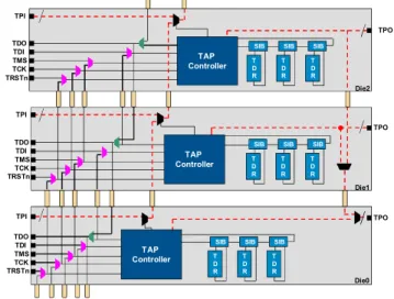
The first type of 3D DFT deals with regular structures as in [6, 7]. The test architecture uses the new IEEE 1687 instead of IEEE 1149.1 as test standard in each die (see fig.5). Multiplexing logic between test pads and test TSVs is used for switching test paths sinks and sources after stacking. For instance, the TDI pad on the top die is used to input test data to this tier before bonding, while test data are transported to this die from the die below after bonding.
TCK TDI TMS TDO TRSTn TCK TDI TMS TDO TRSTn TCK TDI TMS TDO TRSTn T D R SIB T D R T D R SIB T D R SIB T D R T D R SIB T D R TPI TPI TPO TPO SIB T D R TAP Controller TPI TPO T D R Die1 Die2 Die0 TAP Controller SIB SIB SIB SIB TAP Controller
Figure 5. IEEE 1687 based 3D DFT architecture
Each individual die can embed a variety of DFT logic controlled from its TAP controller and associated Test Data Registers (TDRs). The proposed DFT architecture requires that all stacked dies are equipped (1) with a JTAG interface (TDI, TDO, TMS, TCK, optional TRST) as a test access mechanism in order to build the 3D DFT chain, and (2) a TAP controller to build around it IEEE 1687 circuitry: Segment Insertion Bit (SIBs) and associated TDRs..
In order to provide many-bit test data to the tiers after stacking, and thus shorten the test time thanks to concurrent testing of several IPs, each die must be equipped with parallel test inputs. A boundary scan solution with a parallel test access mechanism can be found in [18].
The detailed control of the JTAG Multiplexers is out of the scope of this paper. It could be done with additional configurations registers as currently proposed in IEEE 1838 [8] or it could be optimized using an automatic die-detection mechanism as proposed in [19, 20] but with the limitation of having a static concatenated TAP serial chain.
B. Heterogeneous 3D DFT architecture
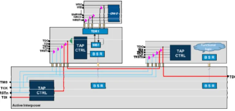
Stacked 3D-ICs may have an irregular test structure; i.e. dies do not embed the same test infrastructure. Figure 6 gives an example of a 2.5D circuit (dies stacked on an interposer) with 3 stacked dies: die_0 (left) is JTAG compliant, die_1 (middle) has a 3-bit test interface (test start, test enable, test result), and die_2 (right) has a IEEE 1500 wrapper.
Figure 6. 3D DFT Architecture of a 3D circuit on passive interposer
Die_0 has been modified in order to manage the test of all the dies in the 2.5D system. A gateway register allows a dynamic configuration of the test infrastructure. Die_0, die_1 and die_2 can be concurrently or serially tested thanks to the SIBs. Die_0 embeds the IEEE 1687 infrastructure: the TAP controller, an IR and a decoder. Die_1 and Die_2 are considered as instruments. We note that the signals WSI and WSO of the IEEE 1500 interface of die_2 are connected directly to the active scan-path and not through latches of the TDR_2 [21].
C. Comparison between both architectures
As a summary, the first test architecture shown in Fig.5 manages the test of uniform 3D circuits where all stacked dies have the same test interface (IEEE 1149.1 in our case). Test signals are transmitted from the bottom die to the top die using TSVs as elevators. Each die embed IEEE 1687 infrastructure which enables test pattern retargeting and enhance test time optimization which will be explained in more details in the next section.
The second test architecture shown in Fig.6 manages the test of heterogeneous 3D circuits such as 2.5D circuits where dies are stacked on passive interposer and have different test interfaces. In this later case, one die should embed a IEEE 1149.1 test interface and a IEEE 1687 specific circuitry to be considered as the master die. The other dies will be considered as slaves and are accessed through the master die as instruments.
The 2 proposed test architectures can be mixed for complex 3D circuits with multi-tower stacked dies: each tier should have an IEEE 1149.1 test interface and establish the serial connection to its adjacent tiers, and within the tier one die can be used as a master die to manage the test of its adjacent dies.
Figure 7. 3D DFT Architecture for a multi-tower 3D IC
An example of a multi-tower 3D SIC is shown in Fig.7, where two dies are stacked within an active interposer and one die stacked on the top of another die.
The interposer with the 2 dies above it forms a serial chain of JTAG TAP controllers. The top-left die embeds IEEE 1687 logic that manages the test of the die above it which has an IEEE 1500 wrapper and considered as a slave of that die. The example shows that the uniform test architecture was used for the interposer with 2 dies and the heterogeneous test architecture was used to handle the test of a die stacked above another die. This proves the complementarities of the two proposed 3D DFT architectures.
D. Features of our proposed 3D DFT architecture based on IEEE 1687and automatic die-detection mechanism
In addition to enabling the test of all the components of the 3D SIC at all binding levels, our proposed 3D DFT architecture allows new features. Thanks to the use of the IEEE 1687 logic and associated high level languages ICL and PDL, the 3D DFT architecture allows
¾ High flexibility of the test of instruments thanks to the dynamic control of SIBs and TDRs, which is advantageous in 3D context especially for test scheduling. ¾ Test pattern retargeting by the mean of the ICL and PDL languages at 2 different levels. The first level is intra-die level where patterns can be retargeted from core level to die level[21] and the second level is inter-die level where patterns are retargeted from die level (2D level) to 3D SIC level (3D level) which is also called 2D to 3D test pattern retargeting [22].
¾ Automatic reconfiguration of the test paths of the 3D system thanks to the use of an automatic die detection which allows a dynamic reconfiguration of test paths during any testing level: pre-bond, mid-bond or post-bond without requiring any configuration in the 3D SIC [20].
E. Implementation of our proposed 3D DFT architetcure on a test chip prototype
We implemented our proposed 3D DFT proposal in a real 3D active interposer called INTACT, designed in the CEA/Leti. The INTACT prototype is composed of an active interposer, on which 6 identical dies are stacked.
TCK TDI TMS TRSTn Active Interposer TDO TAP CTRL 1 0 1 0 1 0 1 0 1 0
Figure 8. 3D DFT architecture for the INTACT prototype
The proposed 3D DFT architecture enables the test of all components at all bonding levels, for both the interposer and the stacked dies.
At interposer level, the pre-bond test is done by configuring the multiplexer of the output TDO to select out the interposer’s TDO, and for post-bond (mid-bond) test the multiplexer is configured to drive out the last bonded die’s TDO.
At die level, the pre-bond test is done through pads, multiplexers (in pink color) are configured to select inputs from pads. For post-bond (and mid-bond) multiplexers (in pink color) are configured to select signals from TSVs and then build the serial chain between TAP controllers. The signal TDO of all dies is always driven to the pad and to the TSV.
The JTAG signals: TCK, TRST, and TMS are common to all dies and the interposer. The TDI-TDO chain is formed serially from the interposer to the first dies, to the next, till the last bonded one.
IV. 3DDFTAND NECESSITY OF TEST SCHEDULING
In addition to the challenges of the Design For Test, there are other challenges for 3D SICs. Among them, the thermal issue is probably the most critical one. The vertical heat dissipation paths in 3D SICs are long and cause the increase of temperature in the 3D SIC. High temperature has adverse impacts on the performances of integrated circuits. The interconnect delay becomes slower while the driving strength of a transistor decreases with increasing temperature. Leakage power has an exponential dependence on the temperature and increasing on-chip temperature can even result in thermal runaways.
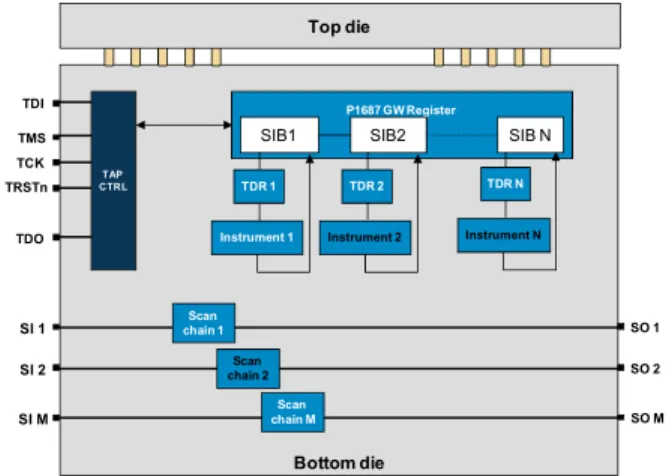
The aim of the 3D test scheduling task is to optimize (lower) the system test time with respect to power consumption and thermal dissipation constraints. For instance, if we consider a tier containing N instruments and M scan chains as shown in Figure. At pre-bond level, a test scheduling can be done by launching the test of all the scan chains and instruments in parallel, with respect to the thermal heating issue at tier-level. SI 1 chain 1Scan SO 1 SI 2 chain 2Scan SO 2 SI M chain MScan SO M TCK TDI TMS TRSTn P1687 GW Register
SIB1 SIB2 SIB N
Instrument 2 TDR 2 Instrument N TDR N TDO TAP CTRL Instrument 1 TDR 1
Figure 8. Pre-bond scheduling, testing all the components
At post-bond level, thermal issues are stronger and the test scheduling by launching all the tests in parallel can be too stressful and damage the circuit.
For instance, if the same tier including N instruments and M scan chains is the bottom die within a 3D stack. The test scheduling performed at pre-bond level can be not efficient at post-bond level because of the power and thermal issues that are accentuated in post-bond level.
Bottom die SI 1 chain 1Scan SO 1 SI 2 chain 2Scan SO 2 SI M chain MScan SO M TCK TDI TMS TRSTn P1687 GW Register
SIB1 SIB2 SIB N
Instrument 2 TDR 2 Instrument N TDR N TDO TAP CTRL Instrument 1 TDR 1 Top die
Figure 9. Post-bond scheduling, testing some instruments and some scan chains
In such a case, running the test of all the instruments and all the scan chains in parallel can be prohibited. The post-bond test scheduling needs to be updated by running the test of only some instruments and some scan chains within the bottom die.
3D scheduling must take into account 1/ the topology of the test bus for feeding test data to scan chains in the cores as discussed above, and 2/ the control architecture for selecting instruments (e.g. BIST engines) through SIBs .As explained in the previous chapter, our proposed 3D DFT architecture is flexible in terms of selecting instruments thanks to the use of the IEEE P1678 and thus does not constrain test concurrency.
Figure 9 presents the proposed design for controlling shift-in and out operations in scan chains with a scan enable signal (SE) if and only if the instrument embedding these scan chains is selected through its SIB.
TCK TDI TMS TRSTn
P1687 GW Register
SIB1 SIB2 SIB N
Instrument 2 TDR 2 Instrument N TDR N TDO TAP CTRL SI 1 SE Scan chain 1 SO 1 SI 2 chain 2Scan SO 2 TDR for Scan chains SI M chain MScan SO M Figure 9. control of scan chains using IEEE 1687 TDR
The length of the associated TDR in this case is equal to the number of scan chains in the target instrument. As a result, each scan chain has a dedicated “SE”. The advantage of the local generation of “SE” signals is to offer more flexibility in terms of test parallelism since scan chains can be used simultaneously or serially.
With this architecture in mind, a test scheduling procedure can be set up since it is now possible to evaluate the area overhead cost of any proposed schedule.
V. CONCLUSION AND FUTURE WORK
We covered different aspects of the DFT challenges to address for 3D ICs. The first aspect concerns the pre-bond test of TSVs where we presented a BIST solution based on ring oscillators. The proposed solution was implemented on a prototype test chip, showing its low implementation cost, and real characteristic measurements on TSV matrices showed that the proposed approach allows to differentiate faulty from fault-free TSVs.
The second aspect of the 3D DFT challenges concerns the test architecture. We proposed an architecture based on IEEE 1687 which allows the test of all the components at all the 3D bonding levels and fulfils other 3D test requirements including 3D test pattern retargeting a dynamic selection of the instruments under test. Moreover the proposed 3D DFT architecture is scalable and can be adapted to specific 3D ICs technologies especially with interposers (passive or active) and/or multi-tower 3D technologies. The last discussed aspect of 3D test challenges concerns the relation between DFT architecture and test scheduling. We have shown that the proposed 3D DFT architecture does not block any test scheduling at any test level and presented and illustrative example of 3D test scheduling that can be done at the different stages of the 3D stacking process. This work opens perspectives towards 3D test scheduling of various instruments “IPs” with physical constraints such as power and thermal issues.
REFERENCES
[1] WideIO JEDEC standard, see http://www.jedec.org/
[2] E.J. Marinissen and Y. Zorian, "Testing 3D chips containing through-silicon vias", in Proc. ITC, 2009, pp.1-11.
[3] Dean L. Lewis, HsienHsin S. Lee "A Scan Island Based Design Enabling Pre-bond Testability in Die Stacked Microprocessors", ITC 2007
[4] Xiaoxia Wu, Paul Falkenstern, Yuan Xie “Scan Chain Design for Three-dimensional Integrated Circuits (3D ICs)”, ICCD 2007
[5] Li Jiang, Lin Huang and Qiang Xu, “Test Architecture Design and Optimization for Three-Dimensional SoCs”, DATE’09
[6] E.J.Marinissen, J.Verbree, M.Konijnenburg, "A structured and scalable test access architecture for TSV-based 3D stacked ICs", in proceedings of VTS 2010, pp. 269 – 274.
[7] E.J.Marinissen, C.-C. Chi, J.Verbree, M.Konijnenburg, “A Standardizable 3D DFT Architecture”, 3D-TEST’10
[8] http://grouper.ieee.org/groups/3Dtest/
[9] Brandon Noia and Krishnendu Chakrabarty, “Pre-Bond Probing of TSVs in 3D Stacked ICs“, in proc International Test Conference 2011, pp 1-10
[10] Brandon Noia and Krishnendu Chakrabarty “Identification of Defective TSVs in Pre-Bond Testing of 3D ICs”, in proc Asian Test Symposium ATS’11, pp 187-194
[11] Li Jiang, Qiang Xu, Bill Eklow and Krishnendu Chakrabarty “3D IC/TSV Probe Test using Adhesive Silicon Interposer” workshop 3D DATE’2012.
[12] Y. Lou, Z. Yan, F. Zhang, and P.D. Franzon, "Comparing Through-Silicon-Via (TSV) Void/Pinhole Defect Self-Test Methods", J. Electronic Testing, 2012, pp.27-38.
[13] Yuan Chen, Cheng-Wen Wu, Ding-Ming Kwai "On-Chip TSV Testing for 3D IC before Bonding Using Sense Amplification", in proceedings of ATS’ 2009, pp 450-455
[14] Tsai M, Klooz A, Leonard A, Appel J, Franzon P, "Through silicon via (TSV) defect/pinhole self test circuit for 3D-IC", in proceedings of 3D’IC, 2009, pp 1-8
[15] Sergej Deutsch and Krishnendu Chakrabarty, ‘‘Non-Invasive Pre-Bond TSV Test Using Ring Oscillators and Multiple Voltage Levels” in proc DATE’2013, pp 1065-1070
[16] G.Di Natale, M.L.Flottes, B.Rouzeyre, H.Zimouche, “Built-In-Self-Test for Manufacturing TSV Defects before bonding” in proc VTS’2014, pp 1-6
[17] Y.FKIH, P.VIVET, B.ROUZEYRE, ML.FLOTTES, G.DINATALE "A 3D IC BIST for pre-bond test of TSVs using ring oscillators" IEEE International New Circuits and Systems Conference (NEWCAS), 2013 [18] Han Ke, Deng Zhongliang, Huang Jianming “Boundary Scan with
Parallel Test Access Mechanism”, ICEMI '09, pp 4-70 - 4-73
[19] Y.Fkih, P.Vivet, B.Rouzeyre, M-L.Flottes, G.Di Natale, J. Schloeffel, “3D Design for Test Architectures Based on IEEE P1687”, workshop 3D Test’13
[20] Y.Fkih, P.Vivet, B.Rouzeyre, M-L.Flottes, G.Dinatale, “A JTAG based 3D DFT architecture using automatic die detection”, IEEE PRIME’13, pp 341 - 344
[21] F.G.Zadegan, U.Inglesson, G.Carlsson, E.Larsson “Reusing and Retargeting On-Chip Instrument Access Procedures in IEEE P1687”, IEEE CEDA 2012
[22] Y.FKIH, P.VIVET, B.ROUZEYRE, ML.FLOTTES, G.DINATALE, J.SCHLOEFFEL “2D to 3D Test Pattern Retargeting using IEEE P1687 based 3D DFT Architectures”, in proc ISVLSI 2014, pp 386-391
View publication stats View publication stats