HAL Id: cea-02044274
https://hal-cea.archives-ouvertes.fr/cea-02044274
Submitted on 21 Feb 2019
HAL is a multi-disciplinary open access
archive for the deposit and dissemination of
sci-entific research documents, whether they are
pub-lished or not. The documents may come from
teaching and research institutions in France or
abroad, or from public or private research centers.
L’archive ouverte pluridisciplinaire HAL, est
destinée au dépôt et à la diffusion de documents
scientifiques de niveau recherche, publiés ou non,
émanant des établissements d’enseignement et de
recherche français ou étrangers, des laboratoires
publics ou privés.
Ideal optical contrast for 2D materials observation using
bi-layer antireflection absorbing substrates
Kevin Jaouen, Renaud Cornut, Dominique Ausserré, Stéphane Campidelli,
Vincent Derycke
To cite this version:
Kevin Jaouen, Renaud Cornut, Dominique Ausserré, Stéphane Campidelli, Vincent Derycke. Ideal
optical contrast for 2D materials observation using bi-layer antireflection absorbing substrates.
Nanoscale, Royal Society of Chemistry, 2019, 11 (13), pp.6129-6135. �10.1039/C8NR09983A�.
�cea-02044274�
Ideal optical contrast for 2D materials observation using bi-layer
antireflection absorbing substrates
Kevin Jaouen,a Renaud Cornut,a,* Dominique Ausserré,b Stéphane Campidelli,a Vincent Deryckea,*
The capability to observe 2D materials with optical microscopy techniques is of central importance in the development of the field and is a driving force for the assembly and study of 2D material van der Waals heterostructures. Such observation of ultrathin materials usually benefits from antireflection conditions associated with the choice of particular substrate geometry. The most common configuration uses a transparent oxide layer with a thickness minimizing light reflection at the air/substrate interface when light travels from air to substrate. Backside Absorbing Layer Microscopy (BALM) is a newly proposed configuration in which light travels from glass to air (or another medium such as water or a solvent) and the antireflection layer is a light-absorbing material (typically a metal). We recently showed that this technique produces images of 2D materials with unprecedented contrast and can be ideally coupled to chemical and electrochemical experiments. Here, we show that contrast can be optimal using double-layer antireflection coatings. By following in situ and with sub-nm precision the controlled deposition of molecules, we notably establish precisely the ideal observation conditions for graphene oxide monolayers which represents one of the most challenging 2D material cases in terms of transparency and thickness. We also provide guidelines for the selection of antireflection coatings applicable to a large variety of nanomaterials. This work strengthens the potential of BALM as a generic, powerful and versatile technique for the study of molecular-scale materials and phenomena.
Introduction
In nanoscience, the capability of observing extremely thin films and materials with a high contrast by optical microscopy is crucial. This is very well illustrated by the role played by optical microscopy from the very early stage of the study of graphene1 and 2D materials.2 Indeed, the use of a transparent antireflection layer of appropriate thickness allowed observing graphene,3-10 graphene oxide11,10 and other 2D materials12-18,9 despite their atomic-scale thickness. This was notably of great value for the identification of the number of layers or the fabrication of van der Waals heterostructures. It is however very important to note that in all these experiments, antireflection coatings were used and optimized in conditions where light travels from the low to the high refractive index of the observation medium (mostly air) and the microscope sample support (mostly silicon or glass) respectively.
The benefits of antireflection coatings in optics have been studied since the end of the nineteenth century and such
coatings are now widely used notably on camera and telescope lenses, eyeglasses, solar cells, optical fibers, and on some optical microscopy substrates.19-21 The most widespread antireflection coatings use transparent layers which cancel the reflected light thanks to destructive interferences. When a high transmittance is not needed in combination with the low reflectance, light-absorbing materials can also be used (alone or in combination with transparent ones).19-24 Stacks of multiple transparent and absorbing materials allow adjusting precisely the optical properties of surfaces in a given range of wavelength and incident angles by selecting the appropriate thickness, refractive index and extinction coefficient of each layer following the classical laws of optics.
Backside Absorbing Layer Microscopy is a recently developed optical microscopy technique which draw its strength from the used of light-absorbing substrates specifically in a reverse microscope configuration, i.e. with light propagating from the high to the low refractive index medium (typically from glass to air or solvent).25-27 The layers used are Anti-Reflecting layers made of Absorbing materials and are thus called ARA layers. For instance, with a single metallic layer deposited on top of a glass substrate used in the backside configuration, there is a preferential metal thickness that allows approaching the ideal antireflection conditions. This thickness depends on the nature of the top medium (air, water, other solvent) and is typically
Please do not adjust margins
close to 7 nm of gold for the glass/gold/air system and of 2-3 nm of gold for the glass/gold/water one. This configuration allows many types of observations with exceptional contrast25,26,28,29 in particular for 2D materials.26 Most importantly, the reverse geometry provides a full half space available for different techniques so that BALM can be easily coupled with other techniques such as electrochemistry.25,26,28,29
However, when implemented in this way (i.e. using a single few-nm thick metallic layer as ARA material), BALM can be further improved. Indeed, even at the most appropriate metal thickness, antireflection conditions can only be approached (for a complete treatment see Ref. 26). The equation nmetal2
-kmetal2 = n0.n3 (with n0 and n3 the refractive indexes of the
bottom (glass) and top media (air, water, solvent)) cannot be exactly satisfied with metals. Therefore, when the metal thickness (emetal) verifies the equation emetal ≈ (λ/4π)(n0
-n3)/(nmetal.kmetal), reflection is reduced to a very low value but is
not cancelled. These layers, that we call near-ARA layers, leave thus room for improvement. In addition, producing stable, homogeneous, ultra-flat and stable metal films on glass in the 2-3 nm thickness range is challenging.30,31 This range is the one adapted for observation in liquids and experiments in water or other solvents are very important for a wide range of studies related to chemical reactivity, bio-sensing, etc. Most of these studies could in principle be further improved if one could design substrates with ARA properties closer to ideal and a thickness higher than 2 nm.
In the following, we show how double antireflection coatings can positively impact the BALM technique and establish the required conditions in different configurations of interest for a broad range of studies, in particular for the observation of 2D materials with enhanced contrast. To do so, we first use the following experiment: the real-time observation and monitoring of the precisely controlled deposition of a thin (0-30 nm) organic layer on a metallic antireflection substrate. Precisely, we follow in-situ and at video rate the light-induced deposition of molecules on gold from a solution of 4-nitrobenzenediazonium tetrafluoroborate (NBDT). Indeed, this compound is soluble in water but light is known to induce the coupling of this molecule forming a water-insoluble species that deposits on the surface.32 Using such photochemical reaction, we benefit from some of the main characteristics of the BALM technique: (i) The organic film is deposited only in the observed area (the size of which can be selected using a diaphragm); (ii) The deposition speed is adjusted by the optical power; (iii) We can record movies of the deposition process allowing very precise extraction of the thickness/contrast relation (in combination with a single AFM calibration step of the final thickness).
Results and discussion
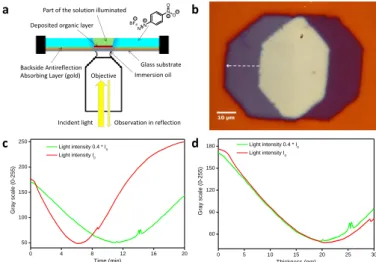
Fig. 1 presents the principle of such experiment and a significant example. A glass slide covered with 3 nm of gold is placed on a reverse microscope equipped with a x63 immersion objective (Fig. 1a) and at t = 0, a solution of NBDT
(10-3 mol.L-1) in water is added on top. The octagonal diaphragm is set at an intermediate size (~50 µm) and the reflected light image is recorded (3 Red/Green/Blue channels with 0-255 gray-scale levels on each). For the sake of clarity and to facilitate thickness measurements at a later step, the position of the substrate is moved laterally by ~20 µm (without stopping data acquisition) after some time (9 minutes in Fig. 1b). After 20 minutes, the solution is replaced with water, the diaphragm is fully open and the global picture reported in Fig. 1b is acquired. One can clearly observe in Fig. 1b the light reflected on the bare gold surface and the light reflected on three areas covered with an organic film with different thicknesses (corresponding to light exposure during 9 min on the right, 20 min in the centre and 11 min on the left part of the pattern).
Figure 1. Light-induced controlled deposition of an organic layer on gold. (a)
BALM configuration of the experiment. (b) Final BALM image showing the organic layer deposition at maximum light intensity. The substrate was moved by ~20 µm at mid-experiment along the arrow direction. (c) Reflected light as a function of time for two light intensities (I0 and 0.4*I0). The plots display the
gray-scale data from the green channel of the camera averaged on a 100x100 pixels area (see text for the impact of this area size), (d) Same as in c after conversion of the time scale into a height scale using AFM measurements.
It is striking that depending on the thickness, the organic material appears either darker or brighter than the gold substrate. The red curve in Fig. 1c reports the raw camera signal as a function of time in the central area (gray-scale of the green channel only, averaged over 100x100 pixels). This red curve brings several key pieces of information: starting at t = 0 from a BALM configuration already selected for its low reflectivity, the signal first decreases by as much as a factor of 3 after ~7 min. It thus provides the first proof that a metal/organic double layer can improve very significantly the antireflection conditions in such BALM configuration. This is important since minimized reflectivity is the key feature allowing very high contrast. Reflectivity in the centre of the image reaches a minimum and then increases again. It yet remains below the initial value (i.e. it constitutes a more efficient antireflection coating than gold alone) for the first 12
0 5 10 15 20 25 30 60 90 120 150 180 Light intensity 0.4 * I0 Light intensity I0 G ray scale ( 0-255) Thickness (nm) 0 4 8 12 16 20 50 100 150 200 250 Light intensity 0.4 * I0 Light intensity I0 G ray scale ( 0-255) Time (min) a c b d
Objective Immersion oil Glass substrate
Incident light Observation in reflection Backside Antireflection
Absorbing Layer (gold) Deposited organic layer
min of the experiment before antireflection efficiency is progressively lost.
The same experiment is then reproduced at a different location of the same substrate using in addition an optical filter that reduces the light intensity to 40 % of its initial value (once again the sample was moved laterally during the experiment after ca. 14 min in this case) and the green curve in Fig. 1c is obtained. After rinsing the sample in water, we measured the different height profiles by AFM (see Fig. S1 in the Electronic Supplementary Information). This allows converting the time scale of Fig. 1c into a height scale in Fig. 1d. As expected, both curves overlap since the deposition rate is simply proportional to the incoming light intensity. But more importantly, this conversion permits to extract precisely the thickness that minimizes light reflection (24 ± 1 nm).
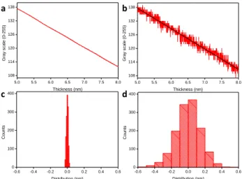
Figure 2. BALM vertical sensitivity for real-time monitoring the deposition of organic ultrathin films. (a) Detail of the 5-8 nm part of the red curve of Fig. 1d corresponding to a 100x100 pixel area. (b) Same data extracted on a single pixel of the movie (red) and linear fit (black line), (c,d) Distribution of the data around the linear fit. The gray value is converted into nm using the slope of the linear fit. The standard deviation is 10 pm and 147 pm in c and d respectively.
At this point, it is interesting to mention the remarkable potential of the BALM technique as a tool to follow in real time the deposition of thin organic layers on surfaces. At a typical recording rate of 25 frames/sec, the intensity evolution can be very precisely analysed. Fig. 2a reports a zoom on the red curve of Fig. 1d (zoom width 3 nm, zoom position 6.5 nm, 100x100 pixels area corresponding to ~7x7 µm2). The lower panel represents the distribution of the data around the mean slope obtained by a linear fit and shows a standard deviation as low as 10 pm. More importantly, when the gray-scale value of a single pixel (corresponding to a ~70x70 nm2 area) is plotted (Fig. 2b), the linear decrease of the reflected signal is still very well resolved and the standard deviation of the dispersion is as low as 0.147 nm. This is smaller than the size of the deposited molecules (mass spectrometry data reported in Fig. S2 shows that the film is fully composed of biphenyl molecules resulting from the dimerization of the initial diazonium derivative) and comparable to the surface roughness. It thus proves that molecular-scale changes can be
monitored in real time with exceptional vertical resolution at each individual pixel of images and at video rate. This is notably of particular relevance for the use of BALM as an ultrasensitive chemical- or bio-sensing technique.
Figure 3. Calculated estimation of the reflected light intensity (at λ = 550 nm and
normal incidence) on a 3 nm-gold/second-layer stack. (a) For klayer2 = 0 and as a
function of the second layer thickness and refractive index nlayer2. (b) Thickness of
the second layer giving minimal reflection for different values of nlayer2 and klayer2. The deposition of an organic thin film from a NBDT solution was selected here as a model system for which the light-induced mechanism32 allows a continuous evaluation of the optical characteristics of the metal/organic double layer. However, the results are generic and absolutely not limited to either this particular compound or this particular deposition method. By adjusting the six parameters of the two layers (thickness, real and imaginary part of the complex refractive index of the metal and organic layers) one can indeed select the optical properties of the substrate that are best adapted for a given microscopy experiments. To illustrate this versatility, Fig. 3 reports numerical estimations obtained by computing the reflectivity of the glass/gold/layer2/water stack based on Fresnel equations. It shows the evolution of the light-reflection for 3 nm of gold (with ngold and kgold taken from
33
) as a function of the thickness of a second layer with refractive index (nlayer2, klayer2). The calculations are performed at a single
wavelength (λ = 550 nm) and at normal incidence. Despite these approximations, they qualitatively capture the main features of Fig. 1d. They notably show (Fig. 3a) how the refractive index nlayer2 impacts the ideal layer thickness for
minimal reflection. For nlayer2 ~ 1.55 and klayer2 = 0, the
minimum of reflectivity is obtained for a film thickness of 25-30 nm, in the same range as the experimental value observed in Fig. 1. In Fig. 3b, the thickness that minimizes the reflectivity is plotted as a function of nlayer2 for different values of klayer2
(see Fig. S3 for details on the impact of klayer2). Fig. 3 and S3 can
be used as an indicative guide to select a second layer coating on gold.
The particular examples presented here are relevant for large classes of experiments since: (i) gold layers with a thickness of 3 nm are stable and conductive (in contrast with sub-2 nm gold layers), (ii) klayer2 in the 0-0.3 range includes a huge numbers of
conventional coatings (polymers, oxides...), (iii) klayer2 = 0 yields
a monotonous evolution of the ideal thickness as a function of nlayer2 (Fig. 3b) which, most importantly, is in a range of
thicknesses ideally suited from a practical point of view (i.e. in
5.0 5.5 6.0 6.5 7.0 7.5 8.0 108 114 120 126 132 138 Gray s c ale (0-255) Thickness (nm) -0.6 -0.4 -0.2 0.0 0.2 0.4 0.6 0 100 200 300 400 C ounts Distribution (nm) -0.6 -0.4 -0.2 0.0 0.2 0.4 0.6 0 100 200 300 400 C ounts Distribution (nm) 5.0 5.5 6.0 6.5 7.0 7.5 8.0 108 114 120 126 132 138 Gray s c ale (0-255) Thickness (nm) a b c d 1.4 1.5 1.6 1.7 1.8 0 5 10 15 20 25 30 35 40 45 klayer2 = 0.2 klayer2 = 0.1 klayer2 = 0 2 nd l a yer t h ickne ss a t min imal refle ct io n (nm) nlayer2 0 10 20 30 40 50 0.0 0.2 0.4 0.6 0.8 1.0 Ref lect ed light intensit y (%)
Second layer thickness (nm) n layer2 = 1.7 n layer2 = 1.4 k layer2 = 0 a b
the 15-50 nm thickness range adapted to spin-coating, evaporation and other deposition techniques, including grafted chemical or biological layers for surface functionalization).
Note, that only the red curve in Fig. 3b is compatible with the data in Fig. 1, which was expected for a fully transparent organic layer (klayer2 = 0). This illustrates how BALM could in
principle be used to provide a quick estimate of (n, k) values for arbitrary coating layers on gold. A quantitative evaluation of the accuracy of such strategy requires the precise knowledge of additional experimental parameters (notably the λ-dependence of the n and k values of ultrathin gold films) and is beyond the scope of this article.
Having established how double-layer metal/organic substrates improve antireflection performances, we now show how this can be used to obtain contrast enhancement for the observation of materials at the nanoscale. For such illustration, we selected graphene oxide (GO) as a model system because it is an important material in nanoscience and in particular in the field of energy conversion and storage.34,35 In addition, contrarily to graphene, reduced-graphene-oxide (r-GO) and most 2D materials (such as MoS2), GO is transparent. It is thus
a challenging material for optical microscopy making contrast enhancement particularly important (note that as stated in the introduction, the use of transparent antireflection coatings in the conventional observation direction and in air-only was already reported for GO11,14). We showed in Ref. 26 how GO behaves on a metallic ARA single layer in BALM experiments, which helps highlighting the advantages of double-layers. In particular, it was shown that GO flakes usually appear with a negative contrast (darker that the substrate), which was indicating room for improvement towards better ARA layers. As a last advantage, GO monolayers of very large lateral size and very limited number of folds and wrinkles can be deposited on any substrate, using for example the method reported in Ref. 36 and used here.
Figure 4. BALM images of GO flakes on gold extracted from a movie (green channel
data from movie_1 in ESI) recorded during the controlled deposition of an organic layer. The only correction to the raw data is as follows: the 0-255 gray scaled range was restricted for clarity to 0-128, 0-96, 0-64 for the 3 images respectively. This simply compensates for the progressive darkening of the images as the reflection decreases, but does not impact contrast values. (a) At t = 0 s, C = -0.046, (b) at t = 50 s, C = -0.119, (c) at t = 156 s, C = -0.167. Raw data and details on contrast extraction are presented in Fig. S4.
Fig. 4 displays three images (green channel) extracted from a full movie (See video_1 in ESI) that records the evolution of the GO visibility on gold during the light-induced deposition of the organic NBDT-based layer. At t = 0, the contrast defined as C =
(IGO-Igold)/(IGO+Igold) is C = -0.046. After 50 s, it is C = -0.119 and
after 156 s, it reached a maximal value of C = -0.167 (see Fig. S4 for details). Strikingly, this is a factor 3.6 higher than in the initial gold-only conditions, which represents a considerable improvement. This evolution of the contrast of GO on gold at the early stage of the deposition of an organic layer can be very well explained using the simple model.
Figure 5. Contrast of monolayer graphene oxide on gold upon molecule deposition. (a)
Contrast calculation for nlayer2 = 1.55 and klayer2 = 0. (b) Light reflected on gold (red
curve) and experimental contrast between gold and GO (blue curve), (c) BALM images at t = 0, t = 3 min 6 sec, t = 5 min 12 sec and t = 6 min 43 sec. GO goes from darker than gold at t = 0 to brighter than gold. The images are extracted from the green channel of a movie. The only correction to the raw data is as follows: the 0-255 gray scaled range was restricted for clarity to 0-196, 0-100, 0-75 and 0-75 for the 4 images respectively. This simply compensates for the progressive darkening of the images as the overall reflection decreases.
Fig. 5a displays the calculated contrast between bare gold (3 nm) and a single layer of graphene oxide (at λ = 550 nm with nGO = 2, kGO = 0.3) on top of gold, as a function of the thickness
of a transparent material deposited above the GO. The nlayer2 =
1.55 and klayer2 = 0 values selected for this organic layer are
those that best represent the deposition from NBDT in Fig. 3 and the (nGO, kGO) values are extracted from Ref. 11. For a very
thin organic film (0-13 nm) the contrast is first enhanced (GO becomes progressively darker) in agreement with Fig. 4. For intermediate thicknesses, the contrast becomes lower (it cancels around 25 nm) and then finally reverses. For ~35 nm, GO should appear much brighter than the gold surface. This calculated behaviour qualitatively matches what is observed experimentally in Fig. 5b, which presents an experiment comparable to the one of Fig. 4 but conducted over a longer time period so as to observe the contrast inversion. The red curve represents the reflected signal on gold and the blue curve the (GO vs. gold) contrast during the deposition of the organic material, extracted from every frame of the movie. The selected images in Fig. 5c highlight the key features: initial contrast enhancement, intermediate point of minimal GO visibility, and contrast inversion. Another important information that can be extracted from Fig. 5b is that: it is not at the minimum of the gold reflectivity (ca. 20 nm in Fig. 5b upper x-axis, dotted red arrow) that occurs the best contrast
a b c 10 µm 0 10 20 30 40 0 3 6 9 12 15 -0.15 -0.10 -0.05 0.00 0.05 0.10 Time (min) C ont ras t GO v s Gold 50 100 150 200 250 Gray s c ale of s upport (0-255) Thickness (nm) a b c 0 10 20 30 40 50 -0.2 -0.1 0.0 0.1 0.2 GO brighter than gold C o n tra st G O vs G o ld
Organic layer thickness (nm)
klayer2 = 0
nlayer2 = 1.55
GO darker than gold
for the observation of GO monolayers (ca. 8 nm in Fig. 5b upper x-axis, dotted blue arrow). It is of great relevance when one wants to select a coating ideally adapted to a specific study.
The methodology used up to here may look specific to the deposition method employed. However, it is important to note that the observed effects are very generic and can be extended in several ways so as to tackle other types of studies in very different contexts. Numerical estimations in Fig. 3 already showed that it is not limited to the organic material used in this study but that minimal reflection conditions exist for most nlayer2 values in a large and relevant range (for the
impact of klayer2 see also Fig S3). We now exemplify the fact
that contrast enhancement: (1) can be obtained with more conventional 2nd layer materials, (2) is not limited to data acquired in water, and most importantly, (3) is also achieved when the material under study (GO in our case) is on top of the second layer coating and not between gold and this second layer. This configuration is of course the one used in conventional microscopy experiments.
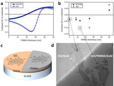
Figure 6. Contrast of GO monolayers above a PMMA/gold antireflection double-layer.
(a) Calculated contrast for a GO monolayer deposited above a PMMA film on 4 nm of gold either in air (open squares) or in water (filled squares) as a function of the PMMA thickness, (b) Experimental contrast of GO monolayers on 3 nm of gold in air and water as a function of PMMA thickness. (c) Principle of the experiment. (d) Example of BALM image (green channel) of GO monolayers directly on gold (left part) and on 13 nm of PMMA on gold (right part). For clarity, the 255 gray scale range was restricted to 0-150.
Fig. 6d displays the main result of the following experiment: a 13 nm-thick layer of PMMA is deposited by spin-coating on 3 nm of gold on glass. Then, stripes in this PMMA film are etched using directive oxygen plasma (reactive ion etching) through a mask. At the last step, GO flakes are deposited on top of this patterned substrate and thus lie either directly on gold or on PMMA above gold as illustrated in Fig. 6c. The image in Fig. 6d is recorded in air. Obviously, the PMMA intermediate layer improves the contrast for the observation of GO monolayer flakes. Such experiment was reproduced for different PMMA thicknesses and the images were acquired both in air and in water. Fig. 6b, reports the measured contrast values while Fig.
6a reports numerical results. In water, with this particular set of parameters, the contrast can only degrade (and get reversed at higher PMMA thicknesses). In air however, there is a very significant contrast enhancement effect in the 20-30 nm range of PMMA. Note that this particular calculation was performed with 4 nm of gold and that the calculated contrast is always higher than the measured one. The difference come from the calculation approximations (single wavelength, normal incidence only vs. high numerical aperture in the experiment) and from the presence of 0.1 nm of chromium as adhesion layer.
From Fig. 4, 5 and 6, it is clear that strong contrast enhancement can be achieved with BALM using double-layer antireflection coating in very different and generic configurations, irrespective of the second layer material (organic or not) and deposition method, stacking order or observation medium (air, water, solvent), one can immediately foresee the benefits of using double inorganic near-ARA layers (typically composed of oxide layers on metal) in place of organic coatings. This opens the way to robust, stable, thickness controlled BALM substrates with improved performances.
Conclusions
In conclusion, we first demonstrated that BALM microscopy can be used to monitor in real time the deposition of molecular films with a precision in the vertical direction of the order of 0.15 nm at the single pixel level and at video rate. Such precision is simultaneously obtained on every pixel of each image of the movie so that textured surfaces and surfaces with pre-deposited materials (typically 2D materials) can be readily studied. In addition, if single-pixel lateral resolution is not required, vertical precision as good as 10 pm is achieved at the 100x100 pixel level (corresponding to a ~7x7 µm2 area). This molecular-scale sensitivity and video-rate operation confirm the high potential of the technique for chemical- and bio-sensing applications.
We then proposed qualitative guidelines for the selection of near-to-ideal double-layer antireflection coatings. By selecting the thickness, refractive index and extinction coefficient of both layers, observation supports optimized for the BALM geometry (light traveling from glass to air or solvent) and adapted to the system under study (observation of transparent or absorbing materials, observation in air or in a solvent, conducting or insulating supports, etc.) can be produced. Beside the enhanced sensitivity, this new study brings an additional asset in terms of surface chemistry: in sensing experiments the material on which sensing probes (typically bio-probes) would be attached can be selected in an extended range of materials to match different functionalization methods.
Finally, double ARA layers lead to very significant contrast improvement for 2D materials. This should facilitate the study of such materials and the fabrication of their heterostructures in an increasing number of laboratories. Moreover, the fact that BALM substrates can be insulating makes possible the
0 10 20 30 40 50 -0.15 -0.10 -0.05 0.00 0.05 0.10 WATER AIR Co n tr a s t GO vs su b s tr a te PMMA thickness (nm) GO on Gold
a
b
c
0 10 20 30 40 50 -0.3 -0.2 -0.1 0.0 0.1 0.2 WATER AIR C o n tr a s t G O v s s u b s tr a te PMMA thickness (nm)d
GO/Gold GO/PMMA/Golddirect coupling of high-contrast observation with electrical measurements. Altogether, this study opens new and exciting possibilities for the use of BALM microscopy as a versatile and powerful tool for nanoscience.
Experimental
BALM. The BALM instrument was setup with Watch Live
S.A.S23, Lyon, France. Microscope cover slides from VWR were used as glass support for single-layer (gold) and bilayers (NBDT/Gold, PMMA/Gold) antireflection absorbing layers. The near-ARA layers are composed of ~0.1 nm of chromium and 3 nm of gold.
GO transfer. The metal coated glass substrates were cleaned
again by exposition to UV-ozone for 30 min and finally washed with isopropanol, dried in a N2 flux and heated at 70°C for 10
min. After the drying process, the slides were placed in a chamber for GO deposition using the so-called bubble deposition technique.36
Organic layer deposition. The BALM slides were placed in a
home-made cell standing on top of a reverse microscope equipped with a Zeiss oil immersion objective, a plan Apo x 63 with numerical aperture NA = 1.40, a Canon EOS 6D camera and an halogen lamp (64655 HLX) filtered with A Thorlabs FESH0700 filter. For the light intensity dependence experiment, a reflective ND filter 0.4 OD from Edmund Optics was added. Water was added on the support to setup the focus, light intensity, spot size and the camera settings. Then water was removed and a movie was started. Then 4-Nitrobenzenediazonium tetrafluoroborate from Sigma-Aldrich (M = 236.92 g.mol-1) at 10-3 mol.L-1 in water was added for 20 min. Movies were recorded with an exposure time of 25 ms and an ISO sensitivity of 800, 2000 and 12800 respectively for experiments at I0 (maximum light intensity), at 0.4*I0 and at
minimum light intensity. At the end of the experiments the solution was removed and the surface was washed twice with DI water.
Conflicts of interest
There are no conflicts to declare.
Acknowledgements
This work is supported by a public grant overseen by the French National Research Agency (ANR) as part of the “Investissements d’Avenir” program (Labex NanoSaclay, reference: ANR-10-LABX-0035). We thank T. Bernard and P. Surugue for technical support.
Notes and references
1. K. S. Novoselov, A. K. Geim, S. V. Morozov, D. Jiang, Y. Zhang, S. V. Dubonos, I. V. Grigorieva and A. A. Firsov, Science, 2004, 306, 666-669.
2. K. S. Novoselov, D. Jiang, F. Schedin, T. J. Booth, V. V. Khotkevich, S. V. Morozov and A. K. Geim, Proc. Natl. Acad. Sci.
USA, 2005, 102, 10451-10453.
3. D. S. L. Abergel, A. Russell and V. I. Fal'ko, Appl. Phys. Lett., 2007, 91, 063125.
4. P. Blake, E. W. Hill, A. H. Castro Neto, K. S. Novoselov, D. Jiang, R. Yang, T. J. Booth and A. K. Geim, Appl. Phys. Lett., 2007, 91, 063124.
5. C. Casiraghi, A. Hartschuh, E. Lidorikis, H. Qian, H. Harutyunyan, T. Gokus, K. S. Novoselov and A. C. Ferrari, Nano Lett., 2007, 7, 2711-2717.
6. Z. H. Ni, H. M. Wang, J. Kasim, H. M. Fan, T. Yu, Y. H. Wu, Y. P. Feng and Z. X. Shen, Nano Lett., 2007, 7, 2758-2763.
7. S. Roddaro, P. Pingue, V. Piazza, V. Pellegrini and F. Beltram,
Nano Lett., 2007, 7, 2707-2710.
8. J. Kim, F. Kim, J. Huang, Mater. Today, 2010, 13, 28-38.
9. S. Khadir, P. Bon, D. Vignaud, E. Galopin, N. McEvoy, D. McCloskey, S. Monneret, G. Baffou, ACS Photon., 2017, 4, 3130−3139.
10. M. Velický, W. R. Hendren, G. E. Donnelly, J. M. Katzen, R. M. Bowman, F. Huang, Nanotechnology, 2018, 29, 275205. 11. I. Jung, M. Pelton, R. Piner, D. A. Dikin, S. Stankovich, S.
Watcharotone, M. Hausner and R. S. Ruoff, Nano Lett., 2007, 7, 3569-3575.
12. H. Wang, F. C. Liu, W. Fu, Z. Y. Fang, W. Zhou and Z. Liu,
Nanoscale, 2014, 6, 12250-12272.
13. M. M. Benameur, B. Radisavljevic, J. S. Heron, S. Sahoo, H. Berger and A. Kis, Nanotechnology, 2011, 22, 125706.
14. D. Bing, Y. Wang, J. Bai, R. Du, G. Wu and L. Liu, Opt. Commun., 2018, 406, 128-138.
15. S. Z. Butler, S. M. Hollen, L. Y. Cao, Y. Cui, J. A. Gupta, H. R. Gutierrez, T. F. Heinz, S. S. Hong, J. X. Huang, A. F. Ismach, E. Johnston-Halperin, M. Kuno, V. V. Plashnitsa, R. D. Robinson, R. S. Ruoff, S. Salahuddin, J. Shan, L. Shi, M. G. Spencer, M. Terrones, W. Windl and J. E. Goldberger, ACS Nano, 2013, 7, 2898-2926.
16. D. J. Late, B. Liu, H. Matte, C. N. R. Rao and V. P. Dravid, Adv.
Funct. Mater., 2012, 22, 1894-1905.
17. H. Li, J. Wu, X. Huang, G. Lu, J. Yang, X. Lu, Q. Xiong and H. Zhang, ACS Nano, 2013, 7, 10344-10353.
18. H. Zhang, ACS Nano, 2015, 9, 9451-9469.
19. S. Chattopadhyay, Y. F. Huang, Y. J. Jen, A. Ganguly, K. H. Chen and L. C. Chen, Mat. Sci. & Eng., 2010, 69, 1-35.
20. M. K. Hedayati and M. Elbahri, Materials, 2016, 9, 497.
21. H. K. Raut, V. A. Ganesh, A. S. Nair and S. Ramakrishna, Energy
Environ. Sci., 2011, 4, 3779-3804.
22. H. Dotan, O. Kfir, E. Sharlin, O. Blank, M. Gross, I. Dumchin, G. Ankonina and A. Rothschild, Nat. Mater., 2013, 12, 158-164. 23. M. A. Kats, R. Blanchard, P. Genevet and F. Capasso, Nat.
Mater., 2013, 12, 20-24.
24. T. Oyama, H. Ohsaki, Y. Tachibana, Y. Hayashi, Y. Ono and N. Horie, Thin Solid Films, 1999, 351, 235-240.
25. D. Ausserre, C. Amra, R. Abou Khachfe, L. Roussille, G. Brotons, L. Vonna, F. Lemarchand and M. Zerrad, J. Nanomed.
Nanotechnol., 2014, 5, 1000214.
26. S. Campidelli, R. Abou Khachfe, K. Jaouen, J. Monteiller, C. Amra, M. Zerrad, R. Cornut, V. Derycke and D. Ausserré, Sci.
Adv., 2017, 3, e1601724.
27. http://www.watchlive.fr
28. J.-F. Lemineur, J.-M. Noël, C. Combellas, D. Ausserré and F. Kanoufi, Faraday Discussions, 2018, 210, 381-395.
29. J.-F. Lemineur, J.-M. Noël, D. Ausserré, C. Combellas and F. Kanoufi, Angew. Chem. Int. Ed., 2018, 57, 11998-12002. 30. A. Kossoy, V. Merk, D. Simakov, K. Leosson, S. Kena-Cohen and
S. A. Maier, Adv. Opt. Mater., 2015, 3, 71-77.
31. R. Malureanu and A. Lavrinenko, Nanotechnol. Rev., 2015, 4, 259-275.
32. W. E. Lee, E. W. Malmberg and J. G. Calvert, J. Am. Chem. Soc., 1961, 83, 1928.
33. L. Gao, F. Lemarchand and M. Lequime, Thin Solid Films, 2011,
520, 501-509.
34. C. Zhu and S. Dong, Nanoscale, 2013, 5, 1753-1767.
35. Y. Zhu, S. Murali, W. Cai, X. Li, J. W. Suk, J. R. Potts and R. S. Ruoff, Adv. Mater., 2010, 22, 3906-3924.
36. J. Azevedo, S. Campidelli, D. He, R. Cornut, M. Bertucchi, S. Sorgues, J.-J. Benattar, C. Colbeau-Justin and V. Derycke, ACS