Comparative study of RF MEMS micro-contact materials
8
0
0
Texte intégral
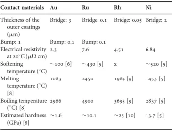
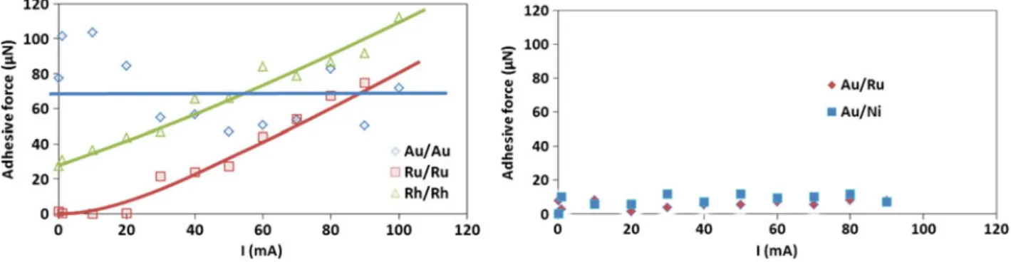
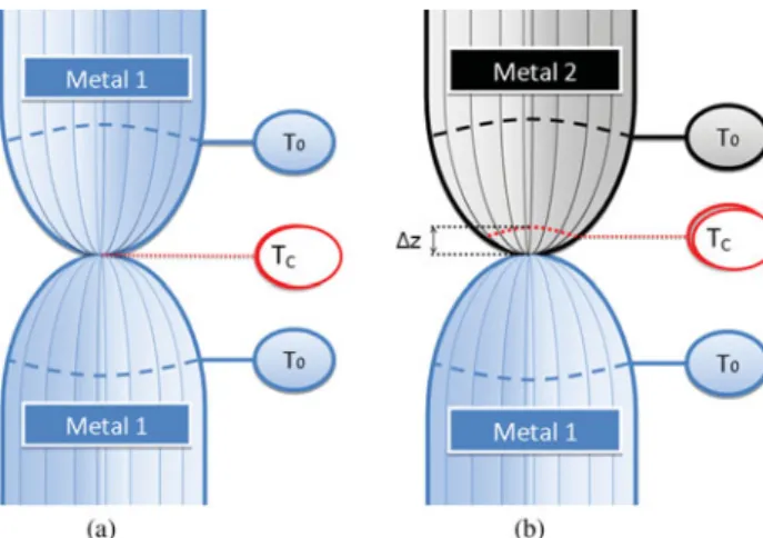
Figure

Documents relatifs