Analysis of stress intensity factors and T-stress to control crack
propagation for kerf-less spalling of single crystal silicon foils
The MIT Faculty has made this article openly available. Please share
how this access benefits you. Your story matters.
Citation Bouchard, P.-O., M. Bernacki, and D. M. Parks. "Analysis of stress intensity factors and T-stress to control crack propagation for kerf-less spalling of single crystal silicon foils." Computational Materials Science 69 (March 2013), pp. 243-250.
As Published http://dx.doi.org/10.1016/j.commatsci.2012.10.033
Publisher Elsevier
Version Author's final manuscript
Citable link http://hdl.handle.net/1721.1/105423
Terms of Use Creative Commons Attribution-NonCommercial-NoDerivs License Detailed Terms http://creativecommons.org/licenses/by/4.0/
Analysis of stress intensity factors and T-stress to control crack
propagation for kerf-less spalling of single crystal silicon foils
P.-O. Bouchard, M. Bernacki, D.M. Parks? a
Mines ParisTech, CEMEF – Centre de Mise en Forme des Matériaux, CNRS UMR 7635, BP 207, 1 rue Claude Daunesse,
06904 Sophia Antipolis Cedex, France.
Email: pierre-olivier.bouchard@mines-paristech.fr Tel: +33 (0)4 93 67 89 21
ABSTRACT: Monocrystalline silicon (called mono silicon) is extensively used in the electronic and solar photovoltaic industries. During the last decade, many new manufacturing processes have been developed to improve solar cells’ efficiency while reducing their cost of production. This paper focuses on a kerf-less technique based on the controlled fracture of silicon foils by depositing an adherent stress-inducing layer on {hkl} cleavage plans. A finite element model (FEM) is defined to study the stress intensity factors (SIF) associated with a pre-crack located at a certain depth from the interface between the silicon substrate and the stress-inducing layer. A parametric study elucidates the dependence of the crack propagation direction on process variables including thickness of the stress-inducing layer, silicon substrate thickness, and pre-crack depth. The use of stress intensity factors and the T-stress characterize the pre-crack
propagation. These results are essential for efficient control of this kerf-less spalling process. Key words: mono silicon, stress intensity factors, T-stress, crack propagation, crack stability.
1. Introduction
During the last decade, a huge effort was made in the photovoltaics (PV) industry in order to reduce the cost of production while improving the efficiency of solar cell systems. In terms of efficiency, it was shown that the peak in terms of efficiency can be reached for silicon foils
thicknesses below 100
µ
m, in the range 40-60µ
m [1]. Cost reduction can be achieved byreducing the cost of materials or decreasing processing costs. Manufacturing thin silicon foils without kerf-loss is thus interesting both in terms of cost reduction and efficiency
improvement. One of the most promising techniques to produce such thin silicon foils without kerf-loss is based on a controlled fracture process of the silicon substrate. A stress-inducing layer is deposited on a suitable crystallographic plane of a moncrystalline silicon substrate. Residual tensile stress in the deposited film induces stress in the silicon substrate that can lead to crack initiation and propagation. This process is achieved below the brittle-to-ductile transition temperature of silicon [2], so that linear elastic fracture mechanics can be used to model silicon brittle fracture. By controlling the film deposition process (e.g., film thickness; magnitude of residual tensile stress, etc.) it is possible to propagate a crack parallel to the interface at a given depth, in the process producing a uniform-thickness silicon foil. Experimental feasibility of such a process was shown first by Dross et al. [3 - 5]. In their process, the stress-inducing layer is made of two metallic layers sequentially deposited from a liquid phase at relatively high temperature. During the cooling stage, the higher thermal expansion coefficient of the metallic layers induces tensile stress in the silicon substrate, causing a crack to initiate and propagate until complete fracture. Controlling the crack stability is quite challenging in this technique, since it relies mainly on the cooling history of the metallic layers. The high temperatures used in this method are problematic for multiple reasons. First, at high temperatures, atomic metal diffusion into the silicon foil can
dramatically reduce the efficiency of photovoltaic conversion; indeed, the first-deposited metal layer serves in part as a diffusion barrier. Secondly, depending on the cooling rate at the highest temperatures, the build-up of elastic strain due to thermal expansion mismatch is partially relieved by viscoplastic flow in the metals, reducing the final stress in the film. More recently, Bedell et al. [6] demonstrated that the same kind of kerf-less controlled fracture process was possible at ambient temperatures. The stress-inducing layer, made of nickel, is deposited using electroplating or by an electroless plating technique [7]. Control of both the thickness and the stress induced in the nickel layer determines the thickness of the fracture depth as well as inhibiting spontaneous fracture of the metal/substrate system. An additional flexible adhesion layer is then applied to the top of the metal layer. By pulling on this adhesive layer, the crack propagates in a controllable manner, parallel to the interface In this paper, a mechanical and numerical study of the fracture process is presented through a detailed analysis of stress intensity factors (SIF). This analysis aims at understanding the influence of different process parameters on the fracture phenomenon. In particular, the influence of the stress induced in the deposited layer, as well as its thickness on the depth of the propagating crack. First, preliminary theoretical studies made on crack propagating in brittle substrates beneath adherent films are presented to introduce fracture mechanics concepts for such configurations. In section 3, we present the configuration studied here. A nickel layer with a given thickness and a given residual tensile stress is deposited on a silicon substrate with an initial pre-crack. Numerical analyses are performed at room temperature
influence of the geometrical/process parameters on the crack propagation direction. Finally, The T-stress is analysed in section 5 to study the stability of the crack propagation direction.
2. Fracture mechanics in a thin film / brittle substrate system
A number of experimental and theoretical studies were conducted in the late 80’s to understand the propagation of cracks in the presence of thin films. Depending on the configuration, these cracks can propagate at the film/substrate interface, or in the substrate, parallel to the interface. Spalling was first investigated under edge loading, and experiments conducted on glass and PMMA (polymethylmethacrylate) showed cracks propagating parallel to the side surface [8]. Thouless et al. [8] showed that for a homogeneous plate containing a sub-surface crack, the stress intensity factors can be given by:
5 . 1 5 . 0 5 . 1 5 . 0 5 . 1 56 . 0 9 . 1 43 . 0 − − − − − = + = Md Pd K Md Pd K II I (1)
where P and M are, respectively, the edge load and edge moment per unit out-of-plane depth,
as shown in Figure 1, d is the crack depth, and KI and KII are the stress intensity factors for
modes I and II, respectively.
Figure 1. Edge loading
As the crack tends to propagate in the direction for which KII=0, it is possible to compute the
crack depth d* at which such a crack exhibits extensive propagation parallel to the adjacent
free surface: P M
d* = 2.7 (2)
Subsequently, Drory et al. [9] investigated the effect of depositing a thin film under residual tension on edge cracks in the substrate. They observed that cracks have a strong tendency to propagate into the brittle substrate, parallel to the interface. Based on superposition principles, it can be shown that generalized edge loading and tensile thin films deposited on a substrate induce equivalent stress intensities at the crack tip. Accounting for the film thickness and elastic properties, Drory et al. [9] showed that it is possible to express the stress intensity
factors as a function of the tensile stress in the film (
σ
0), the crack depth (d), the filmthickness (hf= η
⋅
d), the substrate thickness (hs=τ⋅
d), the modulus ratioΣ
and the moment ofinertia (I) of the resulting bi-layer beam per unit out-of-plane thickness. I depends on the position of the neutral axis of the beam above the substrate crack, and its value is given in [9]. The modulus ratio is
Σ
=Ef/Es for plane stress andΣ
=Ef(1-ν
s2)/Es(1-ν
f2) for plane strainconditions. Ef,
ν
f (resp. Es,ν
s) are the film (resp. the substrate) Young’s modulus and Poissonratio.
The stress intensity factors for edge cracks loaded by tensile films are given in equation 3,
where the parameter
λ
=hs/hf=τ/η representing the thickness ratio between the substrate and(
)
(
)
(
)
(
)
+ Σ + − + Σ = + Σ + + + Σ =λ
λ
λ
λ
η
σ
λ
λ
λ
λ
η
σ
I d K I d K II I 1 217 . 0 558 . 0 . 1 279 . 0 434 . 0 . 0 0 (3)The steady-state cracking in brittle substrates beneath adherent films was then generalized by Suo and Hutchinson in [10].
Based on these results, Xu and Blume [11] extended the analysis of such cracks propagating beneath adherent films by studying the T-stress. The T-stress is the first non-singular term asymptotic expansion of the stress field as a function of stress intensity factors at a crack tip. It represents a normal stress parallel to the crack faces and can be used to study crack
propagation stability and kinking.
Cotterell and Rice [12] modeled the directional stability of crack propagation based on stress
intensity factors and T-stress analyses. They assume that if KII≠0 for a straight crack, then as
overall load magnitude is increased to critical level, the initial incipient cracking will kink
from its original plane at an approximate angle of θ*=-2KII/KI (radian measure). The crack
kinks up if θ*>0 and kinks down if θ*<0. In addition, Cotterell and Rice’s perturbation
solution showed that when a crack propagates “straight ahead” with KII=0 and θ*=0, it is
directionally stable if T<0 but unstable if T>0.
Xu and Blume [11] studied edge cracking in a substrate where loading comes from a tensile film. Assuming straight ahead crack, they found a positive value of the T-stress for a steady-state substrate crack loaded by uniform film tension. According to the Cotterell-Rice criterion [12], the steady-state crack propagation should then be directionally unstable, a result in contradiction with the experimentally steady-state straight cracks propagation observed at a given depth below the interface.
In comment on this issue, Xu and Blume assumed that the stability of the propagating crack depends on the crack length. They hypothesized that, for a short crack, the laminated
composite beam of materials (between the crack and the top surface) is short and dominated by compression, thus inducing a negative T-stress. They assumed further that when the crack
exceeds a given critical length Lc, the composite beam is submitted to bending effect, which
causes a positive T-stress. This T-stress sign and the influence of the crack length will be studied in the last section of this paper.
3. Definition of the numerical configuration
A parallelepiped mono silicon substrate covered with a nickel thin film is considered (Figure
1.a), where hs, ls and ts denote respectively the in-plane thickness, length and out-of-plane
thickness of the mono silicon substrate. The nickel film has the same length and out-of-plane
The numerical geometrical configuration is presented in Figure 1.b, where plane strain conditions are assumed. A symmetry plane is assumed on the right side. Figure 1.c shows the pre-crack configuration, where a, d and w are, respectively, the initial crack length, crack depth, and crack opening.
The aim of such a process being to obtain directionally-stable crack propagation at a given depth d in the Silicon substrate, d is chosen to be the reference length. The value of d will depend on the thickness of the stress-inducing film, but also on the Dundurs’ parameters [13] that are commonly used to characterize the elastic fields in isotropic bimaterial systems:
(
)
(
)
(
1)
(
1)
1 1 + + + Γ + − + Γ = f s f s κ κ κ κ α and(
)
(
)
(
1)
(
1)
1 1 + + + Γ − − − Γ = f s f s κ κ κ κ β . (4)Subscripts f and s refer to the film and substrate materials, respectively. κ = 3 − 4ν for plane
strain and κ = (3 −ν ) (/ 1+ ν ) for plane stress and Γ= µf /µs. Here
µ
andν
are, respectively,the shear modulus and Poisson’s ratio. The parameter α ∈[−1;1] and is a measure of the
stiffness dissimilarity of the two materials. If the film is stiffer than the substrate, then
α
ispositive. Conversely, if the film is more compliant than the substrate,
α
is negative. As shownin [9, 10],
α
has a significant influence on the crack depth and stability, whereas theparameter
β
has only weak influence on the crack depth exhibiting KII =0.In the following, the fixed sample length is ls = 40 mm, and the plane strain assumption
removes the out-of-plane thickness ts from consideration. In the next section, the influence of
in-plane thicknesses hs and hf, as well as the target crack depth, d, will be studied.
Figure 2. a) 3D Geometry of the silicon substrate with a tensile nickel layer deposited on top, b) 2D plane strain configuration, c) pre-crack geometry.
The Abaqus finite element program, part of the SIMULIA package of Dassault Systèmes, was used here. Eight-node quadratic quadrilateral elements (CPE8) were used, and particular attention was paid to the mesh refinement at the crack tip in order to avoid any mesh
perturbations on stress intensity factors computation. The ratio between the size of crack tip element, lt, and the target crack depth is: ltd =4⋅10−2.
Linear elasticity is assumed for both materials, since only small strains are reached and the film deposition process is done at room temperature.
Mono silicon is an anisotropic material whose properties depend on its relative orientation to
the crystal lattice. Its effective Young’s modulus, ESi, ranges from 130 GPa to 188 GPa, and
a) b) c)
ls
ts hf
hs Monocrystalline Silicon Substrate Ni layer
ls
ts hf
hs Monocrystalline Silicon Substrate Ni layer ls/2 hf hs MonoSi substrate Ni layer Sym m e tr y p la n e ls/2 hf hs MonoSi substrate Ni layer Sym m e tr y p la n e a d a d
its Poisson’s ratio,
ν
Si, from 0.048 to 0.40, depending on the orientation of uniaxial tensile loading. Silicon also exhibits modest anisotropy of fracture properties. Depending on theorientation of crack loading and extension, mono silicon’s fracture toughness, KIc, ranges
from 19 to 41 MPa⋅mm1 2. However, as a simplifying assumption, both elastic and fracture
properties will be considered isotropic in this study, and the effects of anisotropy on crack propagation will be studied in a future work. Properties adopted to model mono silicon are given in Table 1; more details on thermomechanical and fracture properties of mono silicon can be found in [14].
The deposited nickel layer is considered as isotropic and homogeneous. Again, this is a simplifying assumption, since the creation of such a nickel layer using physical vapor deposition (PVD), chemical vapor deposition (CVD) or similar techniques [7] can induce thickness heterogeneity within the layer. Regarding anisotropy, the deposited nickel film is polycrystalline, but if the film is thin, there may be a 111 growth-type texture in grains, which might render the nickel as effectively transversely isotropic around a direction parallel to the growth direction.
Chosen values for the nickel Young’s modulus, ENi, and Poisson’s ratio,
ν
Ni, are given inTable 1.
Table 1. Silicon and nickel elastic properties, and silicon toughness
Based on the plane strain elastic mismatch, the Dundurs parameters (4) for this configuration
are:
α
= 0.19 andβ
= 0.067.A symmetry plane is assumed on the right edge of both substrate and film, and the bottom right node of the mesh is fixed in order to suppress rigid body translation.
An initial horizontal tensile stress
σ
0 is applied in the film (see Figure 3.a). This inducedstress can be applied as an initial stress condition in Abaqus. The unloading of this initial tensile stress in the film induces a non-zero stress field in the silicon substrate as can be seen in Figure 3.b.
However, it must be noted that in the real deposition process, the induced tensile stress field is
non-uniform. In particular, the left lateral border of the nickel film (n = -e1) is physically
traction-free, which is thus locally different to the initial stress condition assumed here. But this difference has only local consequences at the extreme top left corner and does not influence the stress field at the crack tip.
In addition, depending on the deposition process used, a gradient of tensile stress may appear across the thickness of the film. The prediction and understanding of this gradient is not straightforward and is a recurrent topic of discussions in the literature. It is commonly accepted that, for different materials, the gradient of tensile stress increases with a reduction of the thickness or an increase of the temperature. However, a more accurate analysis must involve a multi-scale description of the physical phenomenon accounting for the
polycrystalline structure of the deposited material and its evolution during the process [15].
0.3 188 Ni 31.6 0.278 130 Si KIc (MPa.mm1/2)
ν
E (GPa) 0.3 188 Ni 31.6 0.278 130 Si KIc (MPa.mm1/2)ν
E (GPa)Such a modelling is out of the scope of this paper and we assume here that the initial stress condition used is the one that acts at the film/substrate interface.
Last but not least, due to the plane strain assumption, the initial tensile stress field is assumed to be uniaxial, whereas it should be equal biaxial, due to the deposition process. This last assumption can be solved by performing a 3D simulation of the process and by imposing a biaxial initial stress field. But the two first assumptions would require an enhanced analysis of the film deposition mechanisms to get a better description of the stress field. The
computations made in the following are based on a uniform uniaxial initial stress field in the nickel film.
Stress intensity factors (SIF) and T-stress are computed in Abaqus using domain interaction integrals, based on 5 layers of elements surrounding the crack tip. Special attention has been paid to the convergence of the results with respect to mesh size and number of contours.
4. Numerical study of SIF depending on geometrical configuration
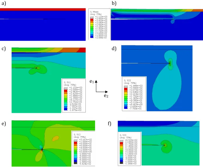
Computations are performed using the implicit version of Abaqus. The initial tensile stress in the nickel film is relaxed while stress tends to increase in the Silicon substrate, in particular at the crack tip.
Figure 3 shows the stress field at the end of the simulation for the following configuration: 8 . 0 = d hf and 3 . 5 = d
a . Figure 3.a shows the initial stress state, in which a uniform tensile
stress of 380 MPa is applied to the film thickness whereas the substrate is stress-free. Figure 3.b shows the final von Mises stress field once the lateral surface traction in the film is relaxed to zero. Significant stress redistribution occurs in the top-left composite beam structure, resulting in stress concentration at the crack tip. A neutral axis also appears in the silicon portion of the laminated beam structure above the crack. Figures 3.c, 3.d, 3.e and 3.f
show, respectively, the
σ
11,σ
22,σ
12 andσ
33 near-tip stress fields. For each figure, the stressscale has been chosen so as to have an optimal view of the stress distribution at the crack tip.
However,
σ
22 is by far the predominant in-plane stress component, being two to three timeslarger than
σ
12 andσ
11. The distribution ofσ
22 in Figure 3.d is characteristic of a stressconcentration at the tip of the crack for a plane strain configuration. However, the stress field is singular for such linear elastic fracture configuration, so that the computed maximal stress value depends on the mesh refinement at the crack tip.
Stress intensity factors have to be computed to study whether the crack is going to propagate
or not. An initiation criterion for mode I is used, e.g. the crack propagates when KI exceeds
the Silicon toughness KIc. The KII=0 criterion is used to define the direction of the crack
kinking. This criterion states that the crack kinks to make KII=0. For a given crack depth, d,
the crack will kink up (towards the interface) if KII is negative and will kink down (away from
the interface) if KII is positive. If KII=0, then the crack will propagate horizontally, in a
4.1. Influence of nickel film thickness for 2 different values of silicon substrate thicknesses:
In this first configuration, we consider a reference geometrical configuration given by: a = 0.4
mm and d = 0.075 mm ( =5.3
d
a ), and we study the influence of silicon substrate and nickel
film thicknesses. The mono silicon substrate thickness hs is equal to 1 or 10 mm. The film
thickness hf varies from 0.01 mm to 0.1 mm. The initial tensile stress applied in the nickel film
is equal to 380 MPa.
Figure 4.a shows the evolution of
K
Iσ
0π
⋅
a
in red (right axis) andK
IIσ
0π
⋅
a
in blue(left axis). Figure 4.b represents the kinking direction (in degrees), based on the KII=0
criterion. For both figures, plain curves correspond to a silicon substrate thickness hs = 10 mm
and dashed curves to hs = 1 mm.
Figure 3. a) Initial stress state, b) von Mises final stress state, c) σσσσ11 stress field at the crack tip, d)
σσσσ22 stress field at the crack tip, e) σσσσ12 stress field at the crack tip and f) σσσσ33stress field at the crack
tip. Configuration hf/d = 0.8 and a/d = 5.3.
a) b)
c) d)
e) f)
e1 e2
Increasing the nickel film thickness induces an increasing of both KI and KII. Increasing the
silicon substrate thickness has almost no effect on KI, but affects significantly KII. This is due
to the fact that a lower substrate thickness allows more bending (max deflection equals to 0.15
mm) than a thicker one (max deflection equals to 0.012 mm). For hs = 10 mm, a value of hf =
0.03 mm would be needed to obtain mode I horizontal crack propagation at a depth d= 0.75
mm, whereas hf = 0.04 mm would be needed to obtain the same cracking in a thinner silicon
substrate of hs = 1 mm.
Figure 4. a)
K
Iσ
0π
⋅
a
andK
IIσ
0π
⋅
a
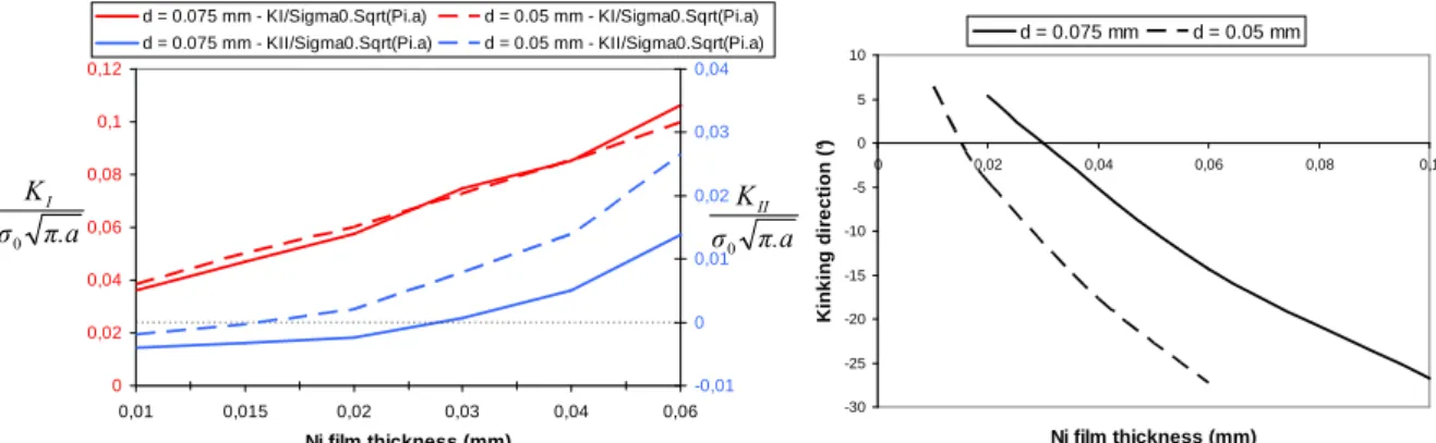
and b) kinking direction (in degrees) as a function of the nickel film thickness for an initial fixed crack length a = 0.4 mm and for two different silicon substrate thicknesses.4.2. Influence of nickel thickness for 2 different values of crack depth: 0.05 mm and 0.075
mm
In this second configuration, the influence of the film thickness is studied for two cracks
depth and for a = 0.4 mm and hs = 10 mm. The crack depth is taken equal to 0.05 mm or 0.075
mm ( =8
d
a or 5.3). The film thickness, hf, varies from 0.01 mm to 0.1 mm. The initial tensile
stress applied in the nickel film is equal to 380 MPa.
Figure 5.a shows the evolution of
K
Iσ
0π
⋅
a
in red (right axis) andK
IIσ
0π
⋅
a
in blue(left axis). Figure 5.b represents the kinking direction (in degrees), based on the KII=0
criterion. For both figures, plain curves correspond to a crack depth d = 0.075 mm and dashed curves to d = 0.05 mm. 0 0,02 0,04 0,06 0,08 0,1 0,12 0,14 0,01 0,015 0,02 0,03 0,04 0,06 0,1 Ni film thickness (mm) -0,01 0 0,01 0,02 0,03 0,04 Si 10 mm - KI/Sigma0.Sqrt(Pi.a) Si 1 mm - KI/Sigma0.Sqrt(Pi.a) Si 10 mm - KII/Sigma0.Sqrt(Pi.a) Si 1 mm - KII/Sigma0.Sqrt(Pi.a) -30 -25 -20 -15 -10 -5 0 5 10 15 20 0 0,02 0,04 0,06 0,08 0,1 Ni film thickness (mm) K in k in g d ir e c ti o n ( °) Si thickness = 10 mm Si thickness = 1 mm π.a σ KI 0 σ π.a KII 0
Figure 5. a)
K
Iσ
0π
⋅
a
andK
IIσ
0π
⋅
a
and b) kinking direction (in degrees) as a function of the nickel film thickness for an initial fixed crack length a = 0.4 mm at two different thicknesses in the silicon substrate.As can be seen on figure 5.a, decreasing the crack depth strongly changes the KII values, and
consequently the direction of crack extension. A 0.05 mm depth crack propagation would only require a 0.015 mm film thickness instead of a 0.03 mm film thickness for a 0.075 mm crack depth.
It is also interesting to notice that for a horizontal (KII = 0) crack propagation at 0.05 mm
depth, the value of KI is equal to 21.43 MPa⋅mm1 2, which is lower than the silicon toughness
taken here equal to KIc = 31.6 MPa⋅mm1 2. This means that for this particular configuration,
the crack will require an additional loading to propagate. Conversely, for a 0.075 mm crack
depth, the value of KI is equal to 31.77 MPa⋅mm1 2, which is slightly higher than silicon
toughness. In this case, the crack can propagate without additional loading.
Controlling crack propagation is essential, in particular in terms of crack propagation
direction stability. When the stress mismatch between the film and the substrate comes from a difference of TCE (Thermal Expansion Coefficient) during a cooling stage (as in [3 – 5]), it is difficult to control the evolution of stress equilibrium because it depends directly on the temperature decrease. This induces a lack of control of stress intensity factors and
consequently a dynamic crack propagation which may not be controlled properly. By working at room temperature and controlling the induced stress in the film layer and the film thickness (as in [6]) it is much easier to avoid spontaneous fracture which can conduct to unstable crack propagation.
This fracture process aims at producing thin homogeneous fractured silicon foils. These computations show that for a target silicon foil thickness (d) and for a given silicon substrate
thickness (hs), it is possible to find a set of nickel film parameters (
σ
0, hf) for which fracturewill occur parallel to the interface, at depth d. In the examples above, we have fixed the nickel film intrinsic stress, and we have studied the influence of the nickel film thickness. The same analysis can be done to find the appropriate intrinsic stress that needs to be applied in the nickel film for a given nickel film thickness. It is important to notice here that the choice of
this couple of parameters (
σ
0, hf) will depend on the deposition technique used.0 0,02 0,04 0,06 0,08 0,1 0,12 0,01 0,015 0,02 0,03 0,04 0,06 Ni film thickness (mm) -0,01 0 0,01 0,02 0,03 0,04 d = 0.075 mm - KI/Sigma0.Sqrt(Pi.a) d = 0.05 mm - KI/Sigma0.Sqrt(Pi.a) d = 0.075 mm - KII/Sigma0.Sqrt(Pi.a) d = 0.05 mm - KII/Sigma0.Sqrt(Pi.a) -30 -25 -20 -15 -10 -5 0 5 10 0 0,02 0,04 0,06 0,08 0,1 Ni film thickness (mm) K in k in g d ir e c ti o n ( °) d = 0.075 mm d = 0.05 mm π.a σ KI 0 σ π.a KII 0
We have studied here the kinking direction of a pre-existing crack depending on the
geometrical configuration. In the next section, the T-stress is analysed in order to check the crack propagation stability.
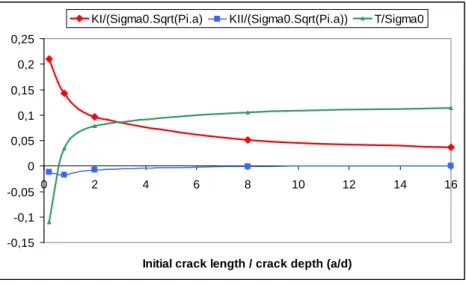
5. Numerical study of T-stress depending on the crack length
As initially showed by Cotterell and Rice [12], the T-stress is a good indicator of the stability of the crack propagation direction. If the T-stress is positive, the crack path is unstable, and may fluctuate around a straight trajectory under the influence of any defects or heterogeneities in the system. If the T-stress is negative, the crack path will keep following its straight
trajectory at the depth corresponding to KII=0. This crack path stability must not be confused
with the crack propagation stability, which is based on the comparison between the strain energy release rate, G, and the G-R curve. In [11], Xu and Blume found a positive value of the T-stress for a crack propagating in a brittle substrate with an adherent tensile film on top. They made the assumption that the sign of the T-stress may depend on the crack length. In order to study the T-stress, we chose the configuration given in the previous section for a
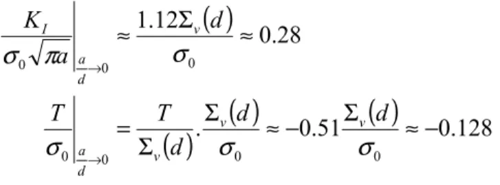
crack depth d= 0.05 mm, and with a nickel film thickness hf = 0.015 mm. The intrinsic stress
in the nickel film is equal to 380 MPa. This configuration is close to the one experimentally tested by Bedell et al. [6]. The T-stress is computed for 5 values of initial crack length, so that the ratio a/d ranges from 0.2 to 16.
Figure 6 shows the influence of the crack length on
a KI π σ0 , a KII π σ0 and 0 σ T . Each of these
values converges as the crack length increases. As indicated in [11], the value of the T-stress is positive, which should induce an unstable crack path. When the ratio a/d tends to 0, the T-stress becomes negative.
When a/d tends to 0 the local stress field becomes similar to the one which would be obtained for a SEC (Single Edge Crack) specimen with a short crack length compared to the specimen
dimensions. For a SEC specimen submitted to a stress
σ
, KI is approximately equaltoKI =1.12σ πa . In the same way T can be written as a function of the applied stress for a
SEC specimen. Based on Harlin and Willis work [16], Hauf et al. [17] and Wang [18] showed that for a SEC specimen, when a/w tends to 0 (where w is the SEC width), the T-stress tends
to -0.51
σ
. In our configuration, the applied stressΣ
v(d) is the vertical stress in Siliconsubstrate without any pre-crack and at a given depth d . For d = 0.05 mm,
Σ
v(d)= 95 MPa.Consequently, for short cracks (a/d
→
0), the ratios0 σ T and a KI π σ0
should tend towards:
( )
( )
.( )
0.51( )
0.128 28 . 0 12 . 1 0 0 0 0 0 0 0 − ≈ Σ − ≈ Σ Σ = ≈ Σ ≈ → → σ σ σ σ π σ d d d T T d a K v v v d a v d a I (5)In [11], Xu and Blume plotted the T-stress of the steady-state crack with respect to Dundurs’
parameter
α
. For a value ofα
= 0.19 they found that the ratio T/σ
0 is approximately equal to0.11. This value is also in good agreement with the value of T/
σ
0 for long cracks in Figure 6which is equal to 0.114.
As assumed in [11], the T-stress is negative for very short cracks (stable crack path) but becomes positive (unstable crack path) when the ratio a/d exceeds a critical value around 0.6. This unstable crack path is not consistent with Bedell et al. [6] experimental results, where a thin homogeneous silicon foil is obtained after peeling.
Figure 6.
K
Iσ
0π
⋅
a
,K
IIσ
0π
⋅
a
and T σ0 as a function of the ratio a/d At this stage, two main assumptions can be formulated to explain these results:- Anisotropic fracture toughness: Cotterell and Rice [12] analysis, obtained under
isotropic assumptions, was extended by Gao and Chiu [19] for anisotropic materials. Gao and Chiu found the same influence of the T-stress sign on the crack path stability, but their demonstration was made under the assumption of a material who has a uniform fracture toughness, which is not the case for mono silicon. For mono silicon, the anisotropy in terms of fracture toughness may have a stabilization influence. If the crack slightly deviates from its straight path, the anisotropy in terms of fracture
toughness may prevent the crack from kinking and stabilize it in the KII=0 direction.
- Peeling process: Bedell et al. [6] thin foils were obtained after peeling using a flexible
handle layer. This peeling process may have a double influence, on the stability of the fracture process and on the crack path stability of the crack when it propagates. As
shown in Figure 6, KI remains lower than KIc for each configuration, meaning that the
system will require additional energy for crack propagation. An additional load is indeed applied in [6] to perform the spalling in a controlled manner. A flexible handle layer is applied on the top of the nickel film. Spalling is performed by pulling on this flexible layer, which induces more energy in the system. If this additional energy is
-0,15 -0,1 -0,05 0 0,05 0,1 0,15 0,2 0,25 0 2 4 6 8 10 12 14 16
Initial crack length / crack depth (a/d)
is too high, the crack propagation may be unstable, meaning that the crack propagates until complete failure without any additional force applied. By controlling the peeling process, it is possible to induce the right amount of energy to allow the crack to propagate on a given length at each peeling step. This additional loading may also influence the T-stress, and thus the crack path stability. In particular because the x position of the loading achieved during peeling is close to the x position of the crack tip.
To understand the influence of this peeling stage on stress intensity factors and T-stress, a new set of computations were carried out, using the same configuration with an initial precrack of a = 0.4 mm length at a depth d = 0.05 mm. Substrate silicon and nickel film
thicknesses are respectively equal to hs = 10 mm and hf = 0.015 mm.
The Abaqus computation is performed in two steps. During the first step, an initial tensile
intrinsic stress
σ
0 = 380 MPa is applied in the nickel film and the stress relaxation iscomputed. During the second step, a force is applied to model the peeling process. This loading condition is idealized here by a concentrated force applied on the top of the nickel
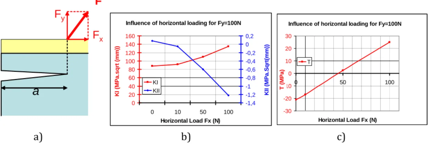
layer at a position x equals to the crack tip position as shown on Figure 7.a. Fy is fixed to 100
N and we study the influence of Fx on stress intensity factors (Figure 7.b) and T-stress (Figure
7.c). Applying such a peeling force does not change the crack propagation direction which
remains equal to 0° because of the small values of KII compared to KI. The peeling force
increases KI to a value higher than KIc. For horizontal forces (Fx) lower than the half of the
applied vertical force (Fy) Figure 7.c shows that the T-stress also becomes negative, meaning
a directionally stable crack propagation. In this case, peeling with an additional force enables
crack propagation (KI> KIc), and the crack would propagate horizontally, with a stable crack
propagation direction.
However, it must be noted that the boundary conditions used for peeling in these simulations
are idealized. For an horizontal force Fx higher than half of the applied vertical force Fy, or for
a force distributed on the top nickel layer, the T-stress remains positive. Bedell et al. [6] do not mention such unstable crack propagation direction. The peeling process is made manually and its influence on crack propagation stability is not discussed.
We also should note that the 3-d situation of a round silicon crystal means that the situation in Bedell et al. [6] peeling may be different still, and mono silicon fracture mechanics based on anisotropic elasticity becomes more relevant.
Figure 7. a) Simplified loading for the peeling stage and Influence of the horizontal force on b) stress intensity factors and c) T-stress
a
F Fx Fy
Influence of horizontal loading for Fy=100N
0 20 40 60 80 100 120 140 160 0 10 50 100 Horizontal Load Fx (N) K I (M P a .s q rt ( m m )) -1,4 -1,2 -1 -0,8 -0,6 -0,4 -0,2 0 0,2 K II ( M P a .S q rt (m m )) KI KII
Influence of horizontal loading for Fy=100N
-30 -20 -10 0 10 20 30 0 50 100 Horizontal Load Fx (N) T ( M P a ) T a) b) c)
6. Conclusion
Controlled spalling of Silicon foils is a promising technique, which enables to obtain very thin silicon foils without kerf-loss. This process is extremely interesting in terms of cost
production since the substrate can be re-used after each spalling. However, controlling the process remains the main issue. If experimental feasibility can be found in the literature [3-6], no detailed fracture mechanics analysis has been published to understand the process and exhibit the more influential geometrical and mechanical parameters. In this paper, the spalling process of silicon was analysed using a numerical investigation of stress intensity factors and T-stress.
The analysis shown that the model is able to predict an horizontal crack propagation parallel to the film/substrate interface for specific geometrical conditions. For a given target silicon layer thickness, the model shows that it is possible to find a couple of film parameters (film
thickness hf and film intrinsic stress
σ
0) to obtain a straight horizontal crack propagation. Thethickness of the deposited film depends both on the Dundurs parameters, and on the target thickness silicon layer. The issue, then, is to be able to get the right amount of intrinsic stress in the film for this thickness so that the system is almost ready to spall.
We also showed that the silicon substrate thickness may influence SIF. This means that silicon thickness has to be accounted for when defining the stress and thickness of the stress-inducing layer. In addition, the homogeneity of this layer can also play a role, and any defects in the layer may disturb the crack path. An analysis of the influence of defects in the film on crack propagation and stability can be found in [11].
The T-stress was analysed in order to study the stability of crack propagation. The T-stress is positive and converges towards a constant value for long cracks, whereas it is negative for small cracks. This means that the crack propagation direction may be unstable for long cracks.
However, this positive value is obtained together with a low value of KI, lower than the
silicon toughness. Bedell et al. [6] used a peeling method with a flexible adhesion layer on top of the nickel film to achieve complete fracture. According to Bedell et al. [6], this peeling process enables to propagate the crack in the Silicon in a controlled manner. It may also have a positive influence on the crack path stability by decreasing the T-stress to a negative value. The peeling stage was modelled here with a simple concentrated force. We have shown that
this additional force was able to increase KI to values higher than KIc and to decrease the
T-stress to a negative value. This implies a directionally stable crack propagation in the silicon substrate. However, peeling forces have to be judiciously chosen in order to get these
conditions (KI>KIc and T<0), whereas peeling conditions are not described in [6].
Further investigations have to be made to improve the control of the process. A 3D analysis of the system would be interesting to study the influence of the out-of-plane direction on the fracture process. In Bedell et al. [6] the contact area between silicon substrate and stress-inducing film is circular whereas it is rectangular in Dross et al. [3] study. This may have a stabilizing impact on the crack propagation direction.
Simulations accounting for anisotropic mechanical properties and toughness of mono silicon will also have to be carried out. The mono silicon crystal orientation seems to play a role on the stability of crack propagation when the stress-inducing layer is obtained by a mismatch of
fracture process occurs at near room temperature. Some preliminary anisotropic computations
showed that accounting for mono silicon anisotropic properties has minor effects on KI but
may change the optimal nickel film thickness (for a given tensile stress in the nickel film) of a few percent to get a straight ahead crack propagation at a target depth.
Finally, a dynamic analysis of the fracture process in mono silicon has to be done to investigate further the evolution of the crack path and its stability regarding
thermomechanical loading conditions and mono silicon orientation [20-23].
Acknowledgements: this work was done within the European project SUGAR funded by the EU's 7th framework program for ICT. The authors are very grateful to IMEC for the
coordination of the project and for interesting discussions related to the spalling process.
7. References
[1] M.A. Green, J.A. Zhao, A. Wang, S.R. Wenham, Very high efficiency silicon solar cells –
science and technology, IEEE Trans. El. Dev. 46(10) (1999) 1940-1947.
[2] P. Hirsch and S. Roberts, The brittle-ductile transition in silicon, Philosophical Maga zine
A, vol. 64(1) (1991) 55–80.
[3] Fr. Dross, J. Robbelein, B. Vandevelde, E. Van Kerschaver, I. Gordon, G. Beaucarne, J.
Poortmans, Stress-induced large-area lift-off of crystalline Si films, Applied Physics A, 89(1) (2007) 149–152.
[4] Fr. Dross, A. Milhe, J. Robbelein, I. Gordon, P.-O. Bouchard, G. Beaucarne, J.
Poortmans, Stress-Induced Lift-Off Method for kerf-loss-free wafering of ultra-thin
crystalline Si wafers, Photovoltaic Specialists Conference, 2008. PVSC '08. 33rd IEEE, 11-16 May 2008 1278-1281.
[5] I. Gordon, F. Dross, V. Depauw, A. Masolin, Y. Qiu, J. Vaes, D. Van Gestel,
J. Poortmans, Three novel ways of making thin-film crystalline-silicon layers on glass for solar cell applications, Solar Energy Materials and Solar Cells, 95(1) (2011) 52-57.
[6] S.W. Bedell, D. Shahrjerdi, B. Hekmatshoartabari, K. Fogel, P. Lauro, N. Sosa, and D.
Sadana, Kerf-less removal of Si, Ge and III-Vs layers by controlled spalling to enable low-cost PV technologies, IEEE J. Photovoltaic, 2(2) (2012) 141-147.
[7] S.W. Bedell, K.E. Fogel, P.A. Lauro, D. Sadana, D. Shahrjedi, Spalling for a
semiconductore substrate, US Patent Application Publication, Appl. N° 12/713,560, 2010.
[8] M.D. Thouless, A.G. Evans, M.F. Ashby, J.W. Hutchinson, The edge cracking and
spalling of brittle plates, Acta Metallurgica, 35(6) (1987) 1333-1341.
[9] M.D Drory, M.D Thouless, A.G Evans, On the decohesion of residually stressed thin
films, Acta Metallurgica, 36(8) (1988) 2019-2028.
[10] Z. Suo, J.W. Hutchinson, Steady-state cracking in brittle substrates beneath adherent
films, International Journal of Solids and Structures, 25(11) (1989) 1337-1353.
[11] Y. Xu, J.A. Blume, Crack interaction and propagation-stability in a thin film/substrate
system, International Journal of Solids and Structures, 30(19) (1993) 2587-2596.
[12] B. Cotterell, J. Rice, Slightly curved or kinked cracks, International Journal of Fracture,
16(2) (1980) 155-169.
[13] J. Dundurs, Elastic interaction of dislocation with inhomogeneities, Mathematical
Theory of Dislocations, ASME (1969) 70-115.
[14] A. Masolin, P.-O. Bouchard, R. Martini and M. Bernacki, Thermo-mechanical and
[15] V. Consonni, G. Feuillet, P. Gergaud, The flow stress in polycrystalline films: Dimensional constraints and strengthening effects, Acta Materialia, 56(20) (2008) 6087-6096.
[16] G. Harlin and J.R. Willis, The influence of crack size on the ductile-brittle transition,
Proc. R. Soc. Lond. A, 415 (1988) 197-226.
[17] D.E. Hauf, D.M. Parks and H. Lee, A modified effective crack length formulation in
elastic-plastic fracture mechanics, Mechanics of Materials, 20 (1995) 273-289.
[18] Y.Y. Wang, A two-parameter characterization of elastic-plastic crack tip fields and
application to cleavage fracture, Ph.D. Thesis, Department of Mechanical Engineering, Massachusetts Institute of Technology, 1991.
[19] H. Gao, C.-H. Chiu, Slightly curved or kinked cracks in anisotropic elastic solids,
International Journal of Solids and Structures, 29(8) (1992) 947-972.
[20] R.D. Deegan, S. Chheda, L. Patel, M. Marder, H.L. Swinney, J. Kim and A. de Lozanne,
Wavy and rough cracks in silicon, Physical Review, E 67 (6) (2003) 066209.
[21] T. Cramer, A. Wanner, P. Gumbsch, Energy dissipation and path instabilities in
dynamic fracture of silicon single crystals, Physical Review Letters, 85(4) (2000) 788-791.
[22] D. Sherman, I Be’ery, From crack deflection to lattice vibrations – macro to atomistic
examination of dynamic cleavage fracture, Journal of the Mechanics and Physics of Solids, 52(8) (2004) 1743-1761.
[23] D. Sherman, Macroscopic and microscopic examination of the relationship between
crack velocity and path and Rayleigh surface wave speed in single crystal silicon, Journal of the Mechanics and Physics of Solids, 53(12) (2005) 2742-2757.