HAL Id: hal-01758581
https://hal.archives-ouvertes.fr/hal-01758581
Submitted on 4 Apr 2018HAL is a multi-disciplinary open access archive for the deposit and dissemination of sci-entific research documents, whether they are pub-lished or not. The documents may come from teaching and research institutions in France or abroad, or from public or private research centers.
L’archive ouverte pluridisciplinaire HAL, est destinée au dépôt et à la diffusion de documents scientifiques de niveau recherche, publiés ou non, émanant des établissements d’enseignement et de recherche français ou étrangers, des laboratoires publics ou privés.
Air-stable anisotropic monocrystalline nickel nanowires
characterized using electron holography
Glenna Drisko, Christophe Gatel, Pier-Francesco Fazzini, Alfonso Ibarra,
Stefanos Mourdikoudis, Vincent Bley, Katia Fajerwerg, Pierre Fau, Myrtil L.
Kahn
To cite this version:
Glenna Drisko, Christophe Gatel, Pier-Francesco Fazzini, Alfonso Ibarra, Stefanos Mourdikoudis, et al.. Air-stable anisotropic monocrystalline nickel nanowires characterized using electron holography. Nano Letters, American Chemical Society, 2018, 18 (3), pp.1733-1738. �10.1021/acs.nanolett.7b04791�. �hal-01758581�
Air-stable Anisotropic Monocrystalline Nickel
Nanowires Characterized using Electron Holography
Glenna L. Drisko,a,b,* Christophe Gatel,c Pier-Francesco Fazzini,d Alfonso Ibarra,e Stefanos
Mourdikoudis,f Vincent Bley,g Katia Fajerwerg,a Pierre Faua and Myrtil Kahna,*
a Laboratoire de Chimie de Coordination, CNRS UPR 8241, 205 route de Narbonne, 31077
Toulouse, France.
b Institut de Chimie de la Matière Condensée de Bordeaux, CNRS UMR 5026, 87 avenue du
docteur Albert Schweitzer, 33608 Pessac, France.
c Centre d’Élaboration de Matériaux et d’Études Structurales, 29 rue Jeanne Marvig, BP 94347,
31055 Toulouse, France.
d Laboratoire de Physique et Chimie des Nano-objets, Institut National des Sciences Appliquées,
135 Av de Rangueil, 31077 Toulouse, France.
e Laboratorio de Microscopias Avanzadas (LMA), Instituto de Nanociencia de Aragon (INA),
Universidad de Zaragoza, 50018 Zaragoza, Spain
f University College London, Healthcare Biomagnetic and Nanomaterials Laboratories, The
g Laboratoire plasma et conversion d’énergie, UMR 5213, Université de Toulouse, CNRS,
Toulouse France.
Abstract: Nickel is capable of discharging electric and magnetic shocks in aerospace materials
thanks to its conductivity and magnetism. Nickel nanowires are especially desirable for such an application as electronic percolation can be achieved without significantly increasing the weight of the composite material. In this work, single-crystal nickel nanowires possessing a homogeneous magnetic field are produced via a metal-organic precursor decomposition synthesis in solution. The nickel wires are 20 nm in width and 1-2 μm in length. The high anisotropy is attained through a combination of preferential crystal growth in the <100> direction and surfactant templating using hexadecylamine and stearic acid. The organic template ligands protect the nickel from oxidation, even after months of exposure to ambient conditions. These materials were studied using electron holography to characterize their magnetic properties. These thin nanowires display homogeneous ferromagnetism with a magnetic saturation (517±80 emu cm-3), which is nearly equivalent to bulk
nickel (557 emu cm-3). Nickel nanowires were incorporated into carbon composite test pieces and
were shown to dramatically improve the electric discharge properties of the composite material.
KEYWORDS. Electron holography, Electric discharge, Ligand stabilization, Magnetism, Nanowires, Nickel
Lightning can and does strike the same place twice. In the case of airplanes, lightning hits each plane on average once per year and enters almost exclusively through the nose. Spacecraft are currently built of carbon fiber-reinforced composites, a material that is lightweight and has desirable mechanical properties, however which suffers from low electrical conductivity. Damage can be caused by low attenuation of electromagnetic radiation and electrostatic discharge (i.e.
lightning strikes),1 creating a security risk in the spacecraft and requiring expensive repairs.
Typically, aluminum or copper are incorporated into the carbon fiber-reinforced composites in order to quickly dissipate the charge. However, copper suffers from oxidation and aluminum from galvanic corrosion. Nickel can effectively dissipate concentrated magnetic and electrical fields, it is resistant to extensive oxidation thanks to the natural formation of a passivating oxide, it has a reasonably low density and is comparatively inexpensive. Conductive Composites sells nickel nanostrandsTM for aeronautics applications, which have been proven to effectively shield
composites from electromagnetic interference and electrostatic discharge-induced damage even after 2 million cycles of fatigue loading.1
Nickel nanostructures have been synthesized in a variety of shapes and sizes by employing several chemical protocols,2-5 yielding nanomaterials with various physical properties. However,
this current report is the first solution based synthesis of individual monocrystalline nanowires. Previously, monocrystalline nickel nanowires have been created via electrodeposition using porous templates, with the smallest nanowire diameter produced to date being 50 nm.6 A similar
technique has been used to produce Au/Ni composite wires using a porous template with a 40 nm diameter.7 Solution chemistry protocols have produced isotropic nanoparticles,8 short nanorods,4
a variety of other structures2 and polycrystalline nanowires.9,10
Monocrystallinity is important because conductivity is related to the number of grain boundaries, as grain boundaries are a barrier to electrical transport.11 Moreover, a protective layer
of nickel oxide forms typically upon exposure to air. Oxidized nickel can be either non-magnetic or antiferromagnetic, radically decreasing the magnetization values compared to those of pure fcc-nickel.12 Long monocrystalline wires of metallic nickel are ideal materials for applications that
We report the metal-organic synthesis of highly anisotropic nickel nanowires having no grain boundaries. The Ni nanowires are obtained through the reduction of a nickel stearate complex using hydrogen gas at 150 °C, in the presence of hexadecylamine and stearic acid (experimental details in SI). The nanowires grow along a particular crystallographic axis (i.e. c), forming a single-crystalline nanowire for the first time using solution chemistry techniques. Using the appropriate relative concentrations of ligand and nickel precursor allowed us to increase the length of the nanowires and to transition away from nanorod-based sea urchin structures. We investigate the magnetic properties of these anisotropic structures using off-axis electron holography and discuss the correlation of such properties with the nanowire structure. The organic ligand layers capping the nickel nanowires protected them from oxidation.
The nickel nanostructures appear either as sea urchin-like structures or as highly anisotropic nanowires, depending on the synthesis conditions (Figure 1, a movie showing the tomography can be found as SI). Anisotropic structures can result from templating or from a difference in the rate of crystal growth along a certain axis. A difference in crystallographic growth rate can occur to minimize the surface energy11 or from capping certain facets with surfactants, ions or solvent.14-16
The sea urchin-like nanostructures are collections of individual nanowires growing from a single nucleus.17 The predominance of a wire versus urchin morphology can be explained using
nucleation and growth kinetics, as has been seen in CoNi nano-objects.18 High nucleation and
growth rates led to CoNi nanowires, where slow nucleation and fast growth led to a sea urchin morphology. The same likely applies to the nickel nanostructures presented here. When the nickel precursor and ligand were highly diluted, nucleation was favored over growth and spherical particles were produced (Figure 2). By decreasing the quantity of solvent, growth was favored over nucleation, producing a dense sea urchin nanostructure (Figure 2b). Upon further
concentrating the solution, a less highly branched nanostructure was observed (Figure 2c), which cannot be explained with nucleation and growth kinetics, but rather to surfactant organization and templating effects. The stearic acid ligand played a major role in the formation of anisotropic nanowires. In the absence of stearic acid, spherical particles were produced (Figure 1b). By increasing the concentration of stearic acid, the anisotropy of the nanoparticles increased (Fig. 1c-d). In this later case, branched nanowires were still present, but unbranched nanowires were commonly found. The nanowires were about 20 nm in width and up to 2 μm in length. Thus, both crystal growth kinetics and surfactant templating seem responsible for the nickel nanostructure morphology.
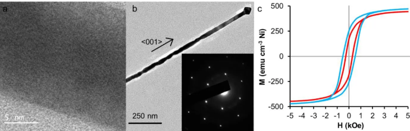
Figure 1. (a) TEM tomographic image of a nickel nanowire with shadows projected in the xy, xz
and yz planes to show the morphology of the nanowire in 3D space. The crystallographic planes are indicated on the illustration in the upper right corner. Nickel nanostructures using a nickel precursor to stearic acid molar ratio of (b) 1:0, (c) 1:2 and (d) 1:6. The white contrast in (c) and (d) are “ghost” images arising from aberrations in the lenses: the corresponding images from diffracted and transmitted beams are displaced relative to one another.
Figure 2. Nickel nanostructures prepared from nickel stearate dissolved in anisole at a
concentration of (a) 5 mM, (b) 50 mM and (c) 150 mM. Under highly dilute conditions spheres appear, while individual nanowires are more prevalent under concentrated conditions. The nickel precursor to stearic acid molar ratio was 1:2. The scale is the same for all images.
The nickel nanowires terminate with a square pyramid tip, with faces of (111) crystallographic orientation, the natural extension of the <001> crystallographic lattice. The sea urchin shape with capped tips has been previously observed in CoNi nanostructures.17,18 The capped tips can be
explained using growth kinetics.18 Towards the end of the synthesis, the nickel precursor is nearly
significantly. Similarly for nickel nanoparticle growth, at the end of the reaction the extremely dilute conditions allow simultaneous growth along other axes, thus generating an arrowhead.
The nickel nanowires are monocrystalline, thus they grew continuously from a nucleus until the nickel precursor depleted (Figure 3a). By measuring the interplanar distances in the diffraction pattern, we determined that the nickel nanorods grew in the <001> direction, and thus the faces present (100) or (111) crystallographic planes. These planes minimize the surface energy.17 No
grain boundaries, crystallographic defects or nickel oxide are visible in the microscopy images (Figure 3a). Normally nickel forms a 2 nm passivating nickel oxide shell upon exposure to air.20
If a 2 nm crystalline oxide shell were present, the diffraction pattern would show differences in the interplane distances between Ni and NiO (Figure 3b inset). The diffraction pattern, which is characteristic of a single crystal lattice, was obtained for the 1085 nm long segment of the nanowire shown in Figure 3b and is representative of the other nanowires analyzed. Thus, the representative TEM images and the associated diffraction pattern prove the nanowires are monocrystalline, and lack a NiO passivating layer. It seems that the organic ligands used are highly effective at protecting the surface from oxidation. Using TGA, it was found that the organic ligands composed 6.8 wt% of the sample. Taking the surface area of the Ni nanowires as 22.6 m2 g-1 and assuming
that the hexadecyl amine and the stearic acid form ion pairs,22 the surface coverage is 6.9 ligand
molecules/nm2. This is an extremely high charge, indicating that there is probably two or more
Figure 3. (a) High resolution transmission electron microscopy image showing the continuity of
the crystal lattice. (b) Electron diffraction of the entire depicted nanowire showing the monocrystallinity of the structure and the alignment with the <001> crystal plane. (c) The hysteresis loop of the SQUID measurement shows the magnetization (M) as a function of the magnetic field strength (H) at 300 K (red) and 2 K (blue). The magnetism of the nickel nanowires was measured after 3 months of exposure to air. The coercivity Hc is 0.54 kOe at 2 K, and 0.31 kOe
at 300 K.
SQUID measurements show that the material presents ferromagnetic properties (Figure 3c). The saturation magnetization at room temperature is equal to 460 emu cm-3, slightly lower than bulk
nickel (557 emu cm-3). This lower value may be due to the coordination of the stearic acid to the
nickel surface.4 SQUID measurements of the magnetism at 2 K and ambient temperature also
confirm the absence of oxidation. An oxide layer around nickel modifies its magnetic properties.22
Nickel is ferromagnetic, where nickel oxide is antiferromagnetic. A thin shell of NiO around a Ni core generates a temperature dependent exchange bias, observed as a horizontal shift of the magnetic hysteresis loop.20,23 As the hysteresis loop corresponding to the field-cooled
nanowires. The nickel nanowires show no evidence of surface oxidation even months after preparation, stored under ambient conditions.
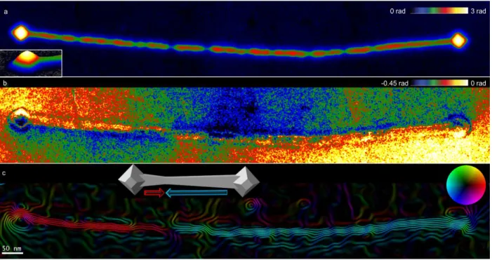
Magnetic and electric maps can be obtained by electron holography, which measures the phase shift of the electron beam after interaction with the electromagnetic field of the sample. Electron holography thus provides the high spatial resolution known to electron microscopy and a quantitative analysis of the local magnetic configuration (Figure 4). The exact magnetic configuration can thus be correlated to the structural properties of a nanostructure, such as the crystal structure, grain boundaries, geometry, and defects. Electron holography measurements can be used to reconstruct the 3D geometry of the nano-object. In our case, these correspond to what was observed with electron tomography images (movie in supplementary information). Electron holography proved that the nickel nanowires are ferromagnetic with a magnetization laid along the nanowire axis due to shape anisotropy (Figure 4).24,25 An off-axis electron holography
experiment in the Lorentz mode was performed using a Hitachi HF 3300C microscope operating at 300 kV and achieving a 0.5 nm spatial resolution in a field-free magnetic environment (less than 10-3 T). All the holograms were recorded in a 2 biprism configuration and the fringe spacing was
set to 1.1 nm in this study. Phase and amplitude images were extracted from the holograms using homemade software with a spatial resolution of 4 nm.
From the measured magnetic phase shift of 0.3 rad, we obtain a Ni magnetization of about 0.65±0.1 T, i.e. 517±80 emu cm-3 in agreement with values obtained from SQUID. The whole
nanowire demonstrated a homogeneous magnetism, although some nanowires exhibited domain walls where the magnetism changed direction. The domain walls show 180° angular displacement and may have been nucleated by saturating the sample during observation. The domain walls were found to exist at the thinnest part of the nanowire, bearing in mind that the nanowire is
monocrystalline, but slightly irregular in width. The domain walls were in the form of pure transverse walls, with no magnetization induction observed in the very center of the domain wall. At this center the magnetization is either parallel to the +Z or –Z direction, as the electron phase shift is only sensitive to the components perpendicular to the electron beam. Vortex states are absent, even in the nanowire arrowheads. The anisotropy of the nanowire is known to cause spin alignment in plane with the wire axis, creating a uniform magnetic state.26
Figure 4. Electron holography of a single, isolated nickel nanowire showing: (a) The mean inner
potential (atomic contribution), with an inset showing the height profile; (b) The magnetic phase @ 4 nm spatial resolution, with a measured phase shift of 0.3 rad in different points of homogeneous thickness across the nanowire; and (c) The vectorial map modulated by the cosine of the magnetic phase (amplified x180) showing a domain wall. The color indicates the direction of the magnetic field, indexed using the color wheel.
To study the electric dissipation of the nickel nanowires, they were dispersed in a polyamide epoxy resin at 0.5, 1 and 5 wt% relative to the quantity of resin, and then infiltrated into a carbon tissue (see supporting information for details). This composite was cured at 80 °C under vacuum, and then cut into test pieces using micromilling (Figure 5b, Figure S1). Potential decay measurements (Figure 5a, Figure S3) were performed on these test pieces to study how an applied surface charge is dissipated by the surface of the material. We can see in Figure 5a that the charge dissipation occurs much more quickly when nickel nanowires are incorporated into the resin relative to the non-doped carbon composite, which has a much higher concentration of electrical charge. The quantity of charge at the beginning of the measurement is already inferior for the nickel loaded samples, as the charge was largely dissipated during the charging phase. The infiltration of the nickel-charged resin into the tissue was not perfectly homogeneous, as can be seen in Figure 5c, which led to inhomogeneities in the dissipation measurements. However, the measured trend was constant: with 5 wt% nickel nanowire loading, the dissipation was much more efficient and complete within around 1 min.
Figure 5. (a) The measured resistance of the carbon composite with variable mass loading of nickel: no nickel nanowires included (yellow); 0.5 wt% (red); 1 wt% (green); and 5 wt% (blue). A
photographic image of the carbon composite test piece after curing (b) at low and (c) high magnification.
In conclusion, we report the first solution-based synthesis of monocrystalline nickel nanowires. The nickel nanowires are 20 nm in diameter and up to 2 μm in length, and are synthesized via the decomposition of metal-organic compounds under air-free and water-free conditions. These nanostructures nucleated and then grew progressively in the <100> direction, where the anisotropy results from a combination of crystal growth kinetics and surfactant templating. There are no grain boundaries within the nanostructure. However, the nanowires are not perfectly homogeneous in width and the thinner portions are susceptible to the formation of magnetic domain walls. Further experiments will show whether the magnetic domain wall was nucleated during observation or whether it was naturally present within the wire. The intensity of the magnetic response is constant and does not show any vortexes. We are currently studying the aging properties of these nickel nanowires in the aerospatial carbon composite test pieces, to study the dissipation behavior upon electric and magnetic shocks with time and under temperature and humidity variations.
Supporting Information. A description of the experimental methods used for nickel nanowire
growth and characterization using microscopy, magnetic measurements and electron holography experiments, the fabrication of test pieces and measurement of their electric dissipation (PDF). A movie showing the 3D tomography of a nickel nanowire (movie clip). The following files are available free of charge.
Corresponding Author
* Glenna Drisko, ICMCB, glenna.drisko@icmcb.cnrs.fr; Myrtil Kahn, LCC, myrtil.kahn@lcc-toulouse.fr
Author Contributions
G.L.D. synthesized all materials and wrote the manuscript. P.F.F. performed transmission microscopy experiments. A. I. performed electron tomography experiments and their
reconstruction. C.G. performed holographic measurements and interpretation. S.M. performed preliminary experiments. V. B. and P. F. performed electric discharge measurements. M.K. and K.F. participated in the design of the synthetic route and financed the research. All authors have read and approved the final version of the manuscript. All authors have given approval to the final version of the manuscript.
Funding Sources
Financial support was provided by the RTRA Sciences et Technologies pour l’Aéronautique et l’Espace. GLD was supported while writing this manuscript by the LabEx AMADEus (ANR-10-LABX-42) in the framework of IdEx Bordeaux (ANR-10-IDEX-03-02); the Investissements d’Avenir program is run by the French Agence Nationale de la Recherche. A.I. thanks the Gobierno de Aragón (Grant E81) and Fondo Social Europeo.
Acknowledgment
Stéphanie Seyrac, Jean-François Meunier and Lionel Rechignat provided technical support. Didier Falandry from CRITT mécanique et composites Toulouse prepared composite carbon samples.
References
1. Mall, S.; Rodriguez, J.; Alexander, M. D. Polym. Composite 2011, 32, 483.
2. Mourdikoudis, S.; Collière, V.; Amiens, C.; Fau, P.; Kahn, M. L. Langmuir 2013, 29, 13491. 3. Cordente, N.; Amiens, C.; Chaudret, B.; Respaud, M.; Senocq, F.; Casanove, M.-J. J. Appl.
4. Cordente, N.; Respaud, M.; Senocq, F.; Casanove, M.-J.; Amiens, C.; Chaudret, B. Nano Lett.
2001, 1, 565.
5. Carenco, S.; Boissière, C.; Sanchez, C.; Le Floch, P.; Mézailles, N. Chem. Mater. 2010, 22, 1340.
6. Tan, M.; Chen, X. J. Electrochem. Soc. 2012, 159, K15.
7. Banobre-López, M.; Bran, C.; Rodríguez-Abreu, C.; Gallo, J.; Vázquez, M.; Rivas, J. J.
Mater. Chem. B 2017, 5, 3338.
8. Bala, T.; Gunning, R. D.; Venkatesan, M.; Godsell, J. F.; Roy, S.; Ryan, K. M. Nanotechnol.
2009, 20, 415603.
9. Xiang, W.; Zhang, J.; Liu, Y.; Hu, M.; Zhao, K.; Guo, H.; Jin, K. J. Alloys Compounds 2017,
693, 257.
10. Lewis, C. S.; Wang, L.; Liu, H.; Han, J.; Wong, S. S. Cryst. Growth Design 2014, 14, 3825. 11. Perry, N. H.; Mason, T. O. Solid State Ionics 2010, 181, 276.
12. Nayak, B. B.; Vitta, S.; Nigam, A. K.; Bahadur, D. Thin Solid Films 2006, 505, 109.
13. Xiang, Y.; Wu, X.; Liu, D.; Feng, L.; Zheng, K.; Chu, W.; Zhou, W.; Xie, S. J. Phys. Chem.
C 2008, 112, 3203.
14. Liu, M.; Guyot-Sionnest, P. J. Phys. Chem. B 2005, 109, 22192. 15. Nikoobakht, B.; El-Sayed, M. A. Langmuir 2001, 17, 6368.
16. Atmane, K. A.; Michel, C.; Piquemal, J.-Y.; Sautet, P.; Beaunier, P.; Giraud, M.; Sicard, M.; Nowak, S.; Losno, R.; Viau, G. Nanoscale 2014, 6, 2682.
17. Soumare, Y.; Piquemal, J.-Y.; Maurer, T.; Ott, F.; Chaboussant, G.; Falqui, A.; Viau, G.; J.
Mater. Chem. 2008, 18, 5696.
18. Ung, D.; Viau, G.; Ricolleau, C.; Warmont, F.; Gredin, P.; Fiévet, F. Adv. Mater. 2005, 17, 338.
19. Vitos, L.; Ruban, A. V.; Skriver, H. L.; Kollár, J. Surface Sci. 1998, 411, 186.
20. Rinaldi-Montes, N.; Gorria, P.; Martinez-Blanco, D.; Amghouz, Z.; Feurtes, A. B.; Barquin, L. F.; de Pedro, I.; Olivi, L.; Blanco, J. A. J. Mater. Chem. C 2015, 3, 5674.
21. Coppel, Y.; Spataro, G.; Collière, V.; Chaudret, B.; Mingotaud, C.; Maisonnat, A.; Kahn, M. L. Eur. J. Inorg. Chem. 2012, 2691.
22. Song, P.; Wen, D.; Guo, Z. X.; Korakianitis, T. Phys. Chem. Chem. Phys. 2008, 10, 5057. 23. Barzola-Quiquia, J.; Lessig, A.; Ballestar, A.; Zandalazini, C.; Bridoux, G.; Bern, F.; Esquinazi, P. J. Phys. Condensed Matter 2012, 24, 366006.
24. Gatel, C.; Bonilla, F. J.; Meffre, A.; Snoeck, E.; Warot-Fonrose, B.; Chaudret, B.; Lacroix, L.-M.; Blon, T. Nano Lett. 2015, 15, 6952.
25. Reyes, D.; Biziere, N.; Warot-Fonrose, B.; Wade, T.; Gatel, C. Nano Lett. 2016, 16, 1230.
26. Biziere, N.; Gatel, C.; Lassalle-Balier, R.; Clochard, M. C.; Wegrowe, J. E.; Snoeck, E. Nano