Commercial Applications of Nanostructures
Created with Ordered Porous Alumina
By
Brendan Christopher Wells
B.S. Materials Science & Engineering B.A. French
Virginia Polytechnic Institute & State University
SUBMITTED TO THE DEPARTMENT OF MATERIALS SCIENCE & ENGINEERING IN PARTIAL FULFILLMENT OF THE
REQUIREMENTS FOR THE DEGREE OF
MASTER OF ENGINEERING IN MATERIALS SCIENCE & ENGINEERING AT THE
MASSACHUSETTS INSTITUTE OF TECHNOLOGY
SEPTEMBER 2004
© 2004 Brendan C. Wells All rights reserved.
i hthc i=apr n da Signature of Author:
Signature of Author: __ _ _
Department
Brendan C. Wells of Materials Science & Engineering August 13, 2004
Certified by: (
Carl V. Thompson II
Stavros Salapatas Professor of Materials Science & Engineering Thesis Supervisor
Accepted by:
Carl V. Thompson II
Stavros Salapatas Professor of Materials Science & Engineering Chair, Department Committee on Graduate Students
MASSACHUSETTS INSTITE OF TECHNOLOGY FEB 16 2005
LIBRARIES
C7w /I _ c · -&Commercial Applications of Nanostructures
Created with Ordered Porous Alumina
By
Brendan Christopher Wells
Submitted to the Department of Materials Science & Engineering on August 13, 2004 in Partial Fulfillment of the Requirements for the Degree of Master of Engineering in
Materials Science & Engineering
Abstract
In the drive from microfabrication to nanofabrication, porous alumina templates may play a key role in technological evolution. Under the right processing conditions, ordered pores can grow in anodic aluminum oxide, which is a high strength, thermally and electrically insulating material. There are many potential applications for porous alumina templates, ranging from the simple fabrication of nanostructure arrays to the more complex processing of components for end-user products such as nano-integrated circuits and gas sensors.
Porous alumina templates can also be processed to have long-range pore ordering on an entire twelve-inch silicon wafer, which may be of unique benefit to processes requiring such pore precision, such as parallel electron beam lithography. The high aspect ratios which can be attained through porous alumina template technology may also offer unique advantages in applications such as field-emission-based devices. As a durable high strength material, porous alumina templates are not limited by extreme process conditions, further extending the reach of their application.
The vast array of applications allows the technology to be financially attractive inside business models ranging from sustaining to disruptive innovation. Porous alumina template technology has the necessary multitude and diversity of attributes to play a crucial role in the future of nanotechnology.
Thesis Advisor: Carl V. Thompson II
Acknowledgments
I've studied electronic materials for the better part of my collegiate career and have only studied nanotechnology on one other occasion outside of my M. Eng. Project: a case study in a senior level materials engineering class back at Virginia Tech. That was my first exposure to nanotechnology, but it was by no means an all-encompassing course. There was much about the nano-world that I had not been introduced to until I started working on my M. Eng. project these past two semesters at MIT. I actually feel quite fortunate to be working with graduate students who have dedicated the last 4 years of their lives working on nanotechnology. I have learned so much just talking to them and listening to their presentations at meetings that even if I did not have to do an M. Eng. project myself, I still would have considered my time with them to be both educational and invaluable.
I paint this background because the work which I am about to present is in no way all from my own head. Those I have worked with have taught me everything I have learned and have provided me the basis from which the following document grew. I am specifically thankful to Professor Carl V. Thompson for his advising as well as his hospitality which was apparent from the beginning of the project. He graciously took me under his wing and I felt from the start as a part of his group. I couldn't imagine working with a better professor. Ramkumar Krishnan has been the vehicle by which I have
learned all I've had to learn in order for this project to be a success. His constant
commitment to me and this project has helped me get as far as I have. I've relied on both
of these men as I pushed towards the final thesis, and they have been an immense help. Additional support has come from the following people: Mom, Dad, Kevin, John, Andrew - I love you all; Sean, John, Adam - Apt. 245 forever; Katie - So this is what Boston is like; and finally, my alma mater - Virginia Polytechnic Institute & State University where my fascination for materials science first began.
Table of Contents
1.0 Introduction ... 8
2.0 Porous alumina template technology ... 9
2.1 Anodization process ... 10
2.2 Process chemistry... 16
2.3 Controlling pore uniform ity... 19
2.4 Reaching beyond lithographic limits ... 25
2.5 Nanostructure fabrication ... 26
3.0 Intellectual property ... 30
4.0 Com peting technologies ... 42
5.0 Porous alumina template applications ... 66
6.0 Business plan ... 75
7.0 Conclusions ... 80
References ... 82
Table of Figures
Figure 2.1: Pictorial description of aluminum anodization and nanopore nucleation. ... 11
Figure 2.2: SEM image of alumina surface after single anodization ... 13
Figure 2.3: Locally ordered pore structure in double anodized alumina ... 14
Figure 2.4: Pore structure in alumina on virgin aluminum. ... 15
Figure 2.5: Anodized flashlight cases created by Anomatic ... 16
Figure 2.6: Atomic description of oxalic acid ... 17
Figure 2.7: Ordered pores separated into domains as a result of double anodization .... 19
Figure 2.8: Inverted pyramid structures etched into a silicon substrate ... 20
Figure 2.9: Al film conformally deposited on pre-patterned silicon ... 21
Figure 2.10: Cross-sectional view of ordered porous alumina on pre-patterned Si ... 22
Figure 2.11: Hexagonally ordered array of porous alumina grown on topographic Si. .. 22
Figure 2.12: Alumina nanopores grown on a patterned silicon substrate ... 23
Figure 2.13: 300 mm wafer, uniformly patterned by interference lithography ... 23
Figure 2.14: Square array of 80 nm dia. pores, processed in phosphoric acid at 86 V... 24
Figure 2.15: Square array of 30 nm diameter pores, processed in oxalic acid at 89 V... 25
Figure 2.16: Effect of pore doubling. ... 26
Figure 2.17: Electrodeposited copper in porous alumina. ... 27
Figure 2.18: Cobalt nanotube in a porous alumina template. ... 28
Figure 2.19: Ordered array of carbon nanotubes ... 28
Figure 3.1: Hexagonal starting point arrangement. ... 32
Figure 3.2: Lithographic pre-patterning of aluminum film ... 33
Figure 3.3: Particle beam technique for fabricating porous alumina templates ... 35
Figure 4.1: Four major steps in photolithography. ... 43
Figure 4.2: Spin-coating of a substrate with photoresist. ... 44
Figure 4.3: Chemical structure of SU-8 ... 49
Figure 4.4: In-situ polymerization of PMMA resist. ... 52
Figure 4.5: Schematic of x-ray generation by electron acceleration ... 53
Figure 4.6: EBL setup ... 55
Figure 4.7: EBL direct-writing techniques. ... 56
Figure 4.8: IBM IC produced with EBL. Note gate dimensions < 100 nm ... 58
Figure 4.9: Dip pen lithography through molecular transport. ... 60
Figure 4.10: Alternating etch and passivation cycles to protect sidewalls ... 62
Figure 4.11: Typical time multiplexing gas flow scheme for DRIE ... 63
Figure 4.12: Trench in silicon fabricated by DRIE ... 64
Figure 4.13: Sidewall of trench fabricated by DRIE ... 64
Figure 5.1: Cartoon of standard cathode ray tube in a television ... 68
Figure 5.2: View of the inside of a television. ... 69
Figure 5.3: Liquid crystal controlling light. ... 69
Table of Equations Equation Equation Equation Equation Equation Equation Equation Equation Equation
2.1 ...
17
2.2 ...
17
2.3 ... 182.4 ...
18
4.1 4.2 4.3 4.4 4.5 44 46 46 47 53...
... .. .. .. .. .. .. .. .. .. .. .. ... .. .. .. .. .. .. .. .. .. .. .. .. ... .. .. .. .. .. .. .. .. .. .. .. .....
... .. .. .. .. .. .. .. .. .. .. .. ... .. .. .. .. .. .. .. .. .. .. .. .. ... .. .. .. .. .. .. .. .. .. .. .. .. ... .. .. .. .. .. .. .. .. .. .. .. ... .. .. .. .. .. .. .. .. .. .. .. .. ... .. .. .. .. .... .. .. .. .. .. ..1.0 Introduction
Nanotechnology is perhaps the buzzword of all buzzwords. There is something intrinsically interesting about the study of phenomena at a scale so small that lengths, diameters, and circumferences can be measured in terms of a relatively small number of atoms. Not only does this science of small make for interesting research, but it may hold many of the world's future technologies as well.
Because many see nanotechnology as the future course of technology, there is an overabundance of research in nearly all conceivable nanoscience areas - from drug delivery to magnetic storage media to nanoelectrical mechanical systems. At the heart of these various nanotechnologies are nanostructures which serve as the building blocks of these applications. As the integral and fundamental part of nanosystems, nanostructures must be developed with the same quality, reliability, and efficiency that current
microstructures and microdevices are produced.
There has been and continues to be a driving force in scientific research to "grow" nanowires, nanodots, nanotubes, and other nanostructures conveniently with controlled
spacing, diameter, and location. This document serves as an evaluation of one specific way in which nanostructures are grown, through the use of ordered porous alumina templates. Of fundamental concern here is an understanding of their production,
application, and benefit over current and future competing technologies.
Whereas microelectronic devices and other structures of "micro" scale have been categorically understood for well over fifty years, the field of nanotechnology and
nanoscience is young. Therefore, any study into specific nano-endeavors must be prefaced with an understanding that the nanotechnology market has not been fully
predicted nor can it be until a plethora of nanotechnologies make it to market. This will take time, and we are currently only at the beginning of a long journey that will take us to the realm of the miniscule, or better yet nanoscule.
2.0 Porous Alumina Template Technology
Many advances in porous alumina template technology (PATT) have occurred over the last ten years, beginning with the work of Masuda et. al.15, of Nippon Telephone and Telegraph in Japan, on double anodization in the mid 1990's. His group noted porous alumina's affinity to grow pores under certain process conditions, and upon further study, they developed a double anodization process that produced pores with short range ordering. Another of the group's major contribution to PATT was their
development and patenting of a stamping technique to allow for long range pore
ordering.8 This work was followed by other groups who noted the interesting aspects and
potential applications of porous alumina. Aiba et al., of Canon Corporation in Japan, studied alternative methods to fabricate a long range ordered porous template.
Specifically, they developed and patented the use of charged particle beams on aluminum surface for this purpose.5
Nielsch et al., at the Max Planck Institute (MPI) in Germany, repeated Masuda et al.'s work by demonstrating ordered porous alumina templates processed through a stamping technique.58 He also successfully worked on ordered magnetic nanowire growth using porous alumina templates.59 Nielsch teamed up with Krishnan, Ross, and Thompson at the Massachusetts Institute of Technology (MIT) to develop a technique to produce long range ordered porous alumina through the use of a pre-patterned silicon
substrate.60 The group noted their success in incorporating inverted pyramids and interference lithography to produce ordered templates. Ohkura et al. independently
studied an identical technique at Canon, and patented the approach.5 7
When Krishnan began concentrating more heavily on porous alumina templates, he again collaborated with Nielsch, Ross, and Thompson in developing pore doubling, a technique to reach beyond lithographic limits for pore spacing. Further work done by the
group included the successful fabrication of ordered copper and gold nanowire growth in long-range ordered porous alumina templates processed by the silicon pre-patterning
technique.6 1
In recent years, Krishnan and Thompson have focused on other template
They have also successfully fabricated ordered arrays of carbon nanotubes using porous alumina templates62, as well as worked on various applications, including parallel
electron beam lithography. A collaboration of Thompson, Ross, and Stellacci at MIT has also resulted in new-found proprietary applications which take advantage of the unique features of porous alumina templates.
It is from these and other past developments which have allowed PATT to be where it is today, a continually thriving research topic and an interesting and marketable idea. What follows is a full description of the most pertinent processing developments and scientific modeling that details the unique benefits of PATT.
2.1 Anodization Process
The method of fabricating porous alumina templates is accomplished through the anodization of an aluminum layer. The purpose of the anodization process is two-fold: to convert the aluminum layer into the much more versatile material alumina; and to grow ordered nanopores in the alumina for use as templates for nanomaterial growth and other applications. Metals form an oxide layer in air, and aluminum, Al, forms alumina, A1203.
This layer is typically only a few nanometers thick and is nonporous. For industrial applications, often a thicker layer of alumina is desired because of the welcome materials properties of alumina which are not present in aluminum, most notably corrosion
resistance. The oxide that forms on aluminum does not flake off, but instead is held strongly in place on the aluminum. One key aspect to alumina is its growth from aluminum under certain processing conditions results in an inherent porosity. This feature is at the heart of porous alumina template technology.
When aluminum is immersed and electrically connected in an electrolytic cell in the presence of an electrolyte, two forms of anodic alumina can form. If the electrolyte
has a pH > 5.0, a nonporous barrier alumina forms. However, in the presence of an acid with much lower pH, porous alumina can form with pore diameters less than 100 nm and lengths on the order of microns. Pore diameter is a function of the electrolytic cell
anodization: phosphoric, oxalic, and sulfuric, with relative diameters, D, given below in
increasing size (all other variable unchanged).
Dphosphoric > Doxalic > Dsulfuric
A layer of barrier alumina constantly separates the aluminum from the electrolyte, and serves as the area of interest for the chemistry of pore growth reactions. Specifically,
at the bottom of the pores, where the pore maintains a significant curvature, the barrier alumina plays the central role in pore development and growth throughout the
anodization process. Figure 2.1 shows the anodization process in detail2.
1st Regime Electrode Elektrolyte AI Al P ~ 3rd Regime 2sd Regime L. 4th Regime
HHn
Figure 2.1: Pictorial description of aluminum anodization and nanopore nucleation.2 ·hillnfi
The aluminum film is cleaned and electropolished prior to anodization to reduce surface roughness, which would otherwise affect pore formation and ordering processes. The polished surface is immediately covered by a native nonporous oxide in air. Because
this oxide is of higher atomic volume than aluminum, very small stress cracks appear on the surface where the native oxide forms. While the exact pore growth mechanism is debated by scientists, many believe that imperfections or cracks present on the surface of the native oxide, which create areas of higher electric field beneath them, are the initial causes of pore nucleation. This can be seen in the 2nd regime of Figure 2.1. The higher
electric field at the bottom of the pore/crack causes a faster dissolution of oxide into the electrolytic solution than at other surface points, resulting in pore generation and preferential growth, as shown in the 3rd regime. The oxide dissolution rate is controlled
by the electric field at the base of the pores, where the curvature is highest (4t h regime),
and the rate of aluminum conversion to alumina is controlled by the average electric field across the barrier oxide/aluminum metal interface.
There are, thus, two chemical processes occurring simultaneously. Aluminum loses electrons, becomes an ion and converts into alumina at the barrier region (st regime) or else continues through the barrier region into solution. Secondly, alumina, which had gained the lost A13+ ions from aluminum is dissolving into solution. Whether the aluminum ions which reach the solution are delivered directly by the dissolution of alumina or instead by diffusion from the aluminum through the alumina, or both, the net effect is conversion of aluminum to alumina, and dissolution of alumina concurrently. The dissolution of alumina happens much faster at surface areas that have higher electric
fields; i.e. where there is higher curvature, and therefore higher electric flux density.
Oxide ions from the electrolyte in solution provide oxygen in the alumina formation. The voltage applied over the electrolytic cell drives A13+ and 02- ions in opposite directions, allowing aluminum to alumina conversion, and barrier alumina dissolution. Pore diameters are kept constant by two limiting phenomena. If pore curvature decreases (creating a larger pore diameter), the flux density at the base of the pores is decreased, and the rate of alumina dissolution slows and the pores would partially fill. If, on the other hand, pore curvature increases (creating a smaller pore diameter), the flux density
After one anodization process, an array of twisted unordered pores exists at the
top of the alumina region, while at the bottom (i.e. the alumina/aluminum interface), the pores are ordered, as shown in Figure 2.2.
Figure 2.2: SEM image of alumina surface after single anodization.2
In order to generate ordered porous alumina, one must control the topography of
the aluminum metal prior to anodization. As described above, it is at areas of higher
curvature that the barrier alumina (formed natively) dissolves most rapidly, leading to
pore growth. While pores are not ordered on the surface of the once-anodized alumina region, they do order at the base of the pores. The 4th regime of Figure 2.1 shows that the
aluminum underneath the barrier alumina layer maintains the topography given to it by
the base of the porous alumina. One way to control the aluminum topography,
introduced by Masuda et al. in the mid 1990s, is by stripping the alumina-off of a sample after anodizing one time. That is, by anodizing a sample of aluminum through a given
thickness of material, and then stripping off the top layer of porous alumina which was created, one is left with an aluminum layer with an ordered topography. After an alumina
topography. A second anodization reconstitutes the chemical reactions described above, but now the pores are ordered at the top of the alumina surface, and proceed to grow as described above. Thus, through double anodization, one can grow locally ordered arrays
of porous alumina.
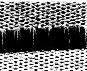
Figure 2.3-4 shows the result of a double anodization.
Figure 2.3: Locally ordered pore structure in double anodized alumina.2
Note that at the base of the pores in Figure 2.4, the aluminum/alumina is curved. One could conceivably remove the alumina and anodize yet again, maintaining the same
Nanoporous alumina
Aluminum
/-Figure 2.4: Pore structure in alumina on virgin aluminum.2
The first anodization process and subsequent alumina strip define a locally ordered topography with hexagonal geometry which, upon a second anodization, results in a locally ordered porous alumina template with the same geometry. While local hexagonal ordering is evident in bulk aluminum anodization, long range ordering is not
present, as shown in Figure 2.2.
Porous alumina template fabrication is not the only application of aluminum
anodization processing. Alumina has long been understood to contain porosity when grown under the right conditions. Because alumina does not flake off, as do other metal oxides such as iron oxide, it has corrosion protection characteristics that are attractive to a
host of industries. Therefore aluminum anodization was developed to grow thicker films
for protecting aluminum components in various products. In these instances, process
conditions prevent porous alumina from growing (which would be susceptible to corrosion). Instead, solely the barrier oxide is grown. Other metals whose oxide is
protective, but are often too thin when grown naturally include titanium, tantalum, and
niobium.
In some applications, porous alumina films are specifically sought. Porosity
allows alumina to be dyed relatively easily, lending to applications in the art world as well as the cosmetics industry. Anomatic is one company whose sole production
products, from lip gloss to flashlights. Figure 2.5 shows a processed example of the
latter.
Figure 2.5: Anodized flashlight cases created by Anomatic.49
The flashlights' brightness and color are controlled during the anodization
processing of the package material.
2.2 Process Chemistry
The nanopore shape and size can be constrained by process chemistry and
electrochemical potential. The following section describes how these two elements affect pore growth.
Though the process design itself involves several clever ideas in the fabrication of
porous alumina, there have been few attempts at studying the underlying relationships between applied voltage, acid molarity, and the quality of pores produced. Up to this point, the research literature only reports on the results obtained using specific setups.
There have been a few empirical relationships that have been reported, but for the most
part the focus has been on perfecting the anodization process by a "guess and test" scheme. Of the many variables in the anodization process, there are two aspects that
First, the chemistry involved is an oxidation reaction whereby the aluminum will readily form an ion by losing three electrons from its 2p orbital so that it can ionically bond with oxygen. The oxygen exists as an ion because it is in solution as an acid. Assuming oxalic acid, C2H204, is the chosen electrolyte in the anodization reaction, then there are two hydroxide ions, OH-, per molecule, as shown in Figure 2.6.
O O
II II
HO-C-C-OH
OXALIC ACID
Figure 2.6: Atomic description of oxalic acid.3
The hydroxide ions float around in the acid under no other constraints. However, when they are subjected to a voltage, they will be drawn to the positive terminal, at which sits the aluminum, and will therefore bond to the aluminum to form alumina. Alumina forms from 3 hydroxide ions, leaving 3 hydrogen ions to return to the solution and float towards the negative terminal. As the aluminum is attacked by the electrolyte, aluminum converts to its own ion A13+. At first A13+ is attracted to the negative terminal, but upon combination with incoming 02- ions, becomes alumina. The oxidation reaction proceeds
as follows:
2Al3+ + 302- -> A1203 (Eq. 2.1)
The overall reaction is as follows:
For safety and practical purposes, oxalic acid is typically used at 0.3 molar solution. The electrolyte concentration has a direct impact on the potential at the electrode/electrolyte interface, according to the Nernst Equation:
E = E0- (RT/zF) * In ([Reduction]/[Oxidation]) (Eq. 2.3)
Where E = actual potential of the electrode, E0= standard potential of electrode couple, R = gas constant, T = absolute temperature, F = Faraday's constant, z = number
of moles of electrons exchanged in reaction, and [Reduction] & [Oxidation] represent the activities (or concentrations for aqueous solutions) of all species on the reduction & oxidation side of the reaction equation, respectively. Therefore, changing the concentration of the electrolyte does have an effect on the actual potential at each electrode, which by extension affects the potential applied across the cell (potential across cell = difference in potentials at each electrode).'6
The second important variable in this process is the applied voltage. There have only been empirical equations drawn from research in this area. "Anodization at low potentials (30-60 V) in 0.3 M oxalic acid at 20 C leads to pore distances of 50-150 nm.
Potentials of 100-195 V can be applied using 10wt% phosphoric acid as electrolyte at 3 C and lead to interpore distances of 300-420 nm."4 Natural ordering is observed at cell
potentials of 25, 40, and 195 V in sulfuric, oxalic, and phosphoric acid solutions, respectively.
Other relationships relating pore spacing to voltage exist as well. A classically held empirical relationship between interpore distances and applied voltage is noted in Equation 2.4,
where 2R equals the pore spacing in nanometers and Va is the applied voltage.
Experimental results show that pore diameters scale at about 30% of the pore spacing. The final product of the anodization process is a block of alumina with pore
spacings on the order of 100 nm and pore diameters on the order of 4 -100 nanometers.
There are, however, several other important features in the anodization process which control these pore dimensions.
2.3 Controlling Pore Uniformity
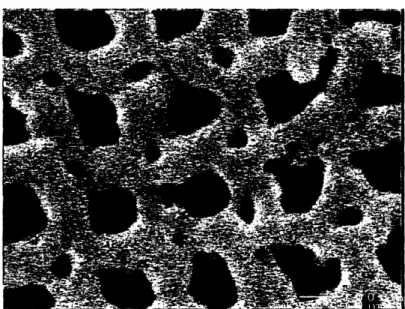
The crucial criterion for creating a uniform template requires that the pores be equispaced, contain vertical sidewalls, and have nearly equal diameters. Typically,
locally ordered pore growth, such as that described above and by other competing
technologies discussed in Chapter 4, result in pore domains. Pores are perfectly ordered
in a hexagonal geometry inside these domains (which look like grains), but along domain
boundaries, there are regions of non-uniformity, where two pores may be nearly
touching, or else have completely combined. Figure 2.7 shows this pictorially.
Pore domain boundaries
While pore uniformity is attempted for most porous alumina template
technologies, many applications simply require short range order. Accomplishing long
range ordering, on the other hand, requires alternate processes to double anodization.
Chapter 4 details several competing technologies which attempt short and long range ordering. Many of these ideas are theoretically possible for pore ordering across a rather sizable area, but are technically unfeasible or simply impractical. Attaining ordered pores
and pore spacing across an entire twelve-inch wafer, for example, has many benefits and
some unique applications, however it requires variations on the processing steps used by
double anodization. There are two predominant methods employed by the MIT group to
attain long range order: substrate pre-patterning; and a heretofore undisclosed procedure
resulting in high aspect ratio porous alumina production.
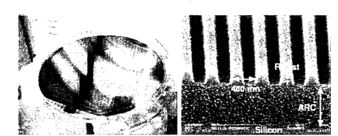
The first method involves a silicon substrate, or other preparation layer, and was independently innovated by Nielsch et. al of MIT and Ohkura et al. of Canon
Corporation, the latter of whom owns a patent on the process57. Though the anodization process requires only aluminum, a silicon substrate allows added versatility and a unique
pore structure control mechanism. The substrate layer is patterned using interference
lithography and wet etched so that an array of inverted pyramid-shaped structures cover the surface of the silicon. Figure 2.8 shows a scanning electron micrograph of the patterned silicon topography.
Aluminum is then deposited over the silicon substrate, and conformally coats the
Si surface, as shown in Figure 2.9.
Figure 2.9: Al film conformally deposited on pre-pattemrned silicon.2
A topography is created on the top of the aluminum which identically matches the
pre-patterned silicon substrate. A very small native aluminum oxide then forms
immediately in air over the deposited aluminum, and the anodization process continues as described previously. In this technique, however, because an ordered topography has
already been established, there is no need for a second anodization. The first anodization causes pore growth at points of high curvature in the alumina barrier layer (which has been transferred through the virgin aluminum, from the pre-patterned silicon substrate).
Figure 2.10 shows a cross-sectional view of anodized alumina on a pre-patterned silicon substrate.
,-? * ~ ~,m c..~~~Tz" ~..,: w ~'-~ '"l ¸,i .: ~ W ,~,: J :.: '",l
- ...
a i··' p
.a
aD.,t~i
-.
~-
-'~~
a_
~
C;
a
US-·~
Figure 2.10: Cross-sectional view of ordered porous alumina on pre-patterned Si.2
Figure 2.11 shows a top-down view of an anodized template first deposited on a
hexagonally arranged Si topography.
b. :*# - - SI
,~
...
,:
-
-- eo
, ;::
--
'e'
Figure 2.11: Hexagonally ordered array of porous alumina grown on topographic Si.
Figure 2.12 shows a cross sectional cartoon of the result of anodization on
Figure 2.12: Alumina nanopores grown on a patterned silicon substrate.2
The physical limit of the pores' length is the thickness up to which a silicon pattern can be transferred to the aluminum film. At a critical thickness, on the order of I
micron, the pattern is no longer distinguishable from surface roughness. This limit still
allows for very good aspect ratio structures to be created using PATT.
One other advantage of this technique is that it allows periodic and identical pore structures to be developed over large areas. Pores are not separated into domains, as in
the case of double anodization. Instead, depressions in the aluminum are equispaced due to the silicon's pre-patterning. It has been demonstrated by Heilmann et al., whose
results are shown in Figure 2.13, that interference lithography can be used to successfully pattern equispaced features across an entire wafer.5 6 Therefore, pre-patterning a silicon
wafer, followed by aluminum deposition and anodization could produce an entire wafer of ordered pores.
I
I
W-1
Figure 2.13: 300 mm wafer, uniformly patterned by interference lithography.55
Filling an entire wafer with ordered pores requires careful selection of pore location geometries. Using the topography-transfer technique described above, the
geometry of pore growth at the surface of the aluminum layer is controlled by the topography of the silicon substrate. Square, rectangular, triangular, or hexagonal
geometries guarantee that an entire surface will be uniformly covered by equispaced nanopores. One advantage of this approach in porous alumina fabrication is that the geometry can be controlled. In double anodization of bulk alumina, only the most stable
hexagonal arrays will grow. However, square and other geometry arrays can be grown
stably on patterned substrates up to specific alumina thicknesses. Most research has concentrated on hexagonal arrays of nanopores because the majority of studies on the subject are geared towards short-range ordering. A square array of aluminum, deposited
on pre-patterned silicon prior to anodization, is shown in Figure 2.9. A hexagonal array
of ordered pores is shown in Figure 2.11.
Another unique advantage of pre-patterning Si to grow ordered arrays of pores in
alumina is that the pore size and spacing can be independently controlled. Whereas Eq.
2.4 and other empirical evidence describe the relationship between applied cell voltage and subsequent pore features and spacings, pre-patterning results in the forced growth of
pores at specific locations due to a patterned topography. Figures 2.14-15 show the
relative ease of pore diameter control using the pre-patterning technique.
.
-, ' A. . _ ... . . . . · . . .. . _ . .
', , . , , ;%,,- , -, SA : ~, . , *. ._ * .; .:'t '; ,.
,:* -a ' ,-: :"-,is -i;s
we
.- '.. ,.* * .,-* ,, , ',a -4 -'a, .. ',Figure array of 8 2.14: Square nm 0 a-t 86 V.2
t * -a a Ok a AVAR a a'- a A A ma a a S
W 3 a *at ' 35 .* .3 *5 * U P * a- 1. 5' i
Figure 2.15: Square array of 30 nm diameter pores, processed in oxalic acid at 89 V.2
Not only does the silicon substrate allow control over the placement of pores in the alumina, but it also allows the template to be integrated into current silicon
technologies in the microelectronics industry. Because silicon is so widespread and is the most common link between devices and components, growing templates on silicon allows for this added benefit.
The second, and perhaps most promising, technique researched by the MIT group follows some of the same principles and techniques as described above, but allows for both very high aspect ratio structures and long range pore ordering. Patents are currently pending.
2.4 Reaching Beyond Lithographic Limits
The more pores that fit on a surface, the more useful the template becomes.
Approaching and surpassing lithographic limits using porous alumina may be possible by way of a technique called pore doubling. Occurring at processing conditions which
include lower electrolytic cell voltages than that given by empirical relationships, such as
Eq. 2.4, pore doubling reduces the distance between pores by growing a second array of
pores offset from a first array. Thus far, however, there have been no successful attempts
deformed. More development is required before this technique can be implemented commercially. Figure 2.16 shows results of the technique.
Figure 2.16: Effect of pore doubling.2
2.5 Nanostructure Fabrication
Fabrication of the porous alumina template constitutes the primary and most
unique step in this process of fabricating nanodevices, however there is much more flexibility in the second process: fabricating nanostructures in the template. At this point, there are several fabrication options, including nanodots6, nanorods, nanowires, and nanotubes. It has been shown2 thus far that each of these structures can be fabricated successfully, and in a relatively straightforward manner. In fact, upon the first successful
fabrication of a porous alumina template with long-range order, the MIT group's first
attempt at depositing nanostructures was successful as well. Because the template serves
as a mold for nanostructure growth, simply depositing (generally done by
electrodeposition) the desired metal (nickel, copper, etc) will yield a metal nanostructure.
deposition is the process of choice. Figure 2.17 shows an array of locally-ordered porous alumina after copper electrodeposition.
Figure 2.17: Electrodeposited copper in porous alumina.2
One way to tailor the dimensions of the nanoparticle is to control the film
thickness of the anodized aluminum. Nanopores will only grow through the oxidized
metal until they reach the silicon barrier layer (or more commonly until the reaction is
stopped in the experiment). Thus, pits or long pores can be fabricated and then filled
with metal to allow for nanodots or nanorods and nanowires. Additionally, carbon and other types of nanotubes can be grown as has been suggested in the literature2' 7. Figure 2.18-19 show SEM micrographs of a cobalt nanotube, and an ordered array of carbon
Co
A1203
Figure 2.18: Cobalt nanotube in a porous alumina template.2
Figure 2.19: Ordered array of carbon nanotubes.2
Two powerful techniques, one of which is already patented, but the other of which may prove to be more valuable to template processing, have been employed
variability of nanostructure growth. The proprietary techniques developed at MIT also offer other added benefits, such as high aspect ratio attributes.
3.0 Intellectual Property
The intellectual property landscape for PATT is scattered, at best, with most patents covering specific ways to fabricate templates and structures. There are many patents on various template processing ideas, fewer on nanostructures, and an extreme few on devices. There may only be one patent that prohibits commercialization of the techniques employed by the MIT group without licensing.
Porous alumina template technology patents are stratified in three layers. First, there are patents pertaining to the various techniques to grow alumina templates. There are many such patents, all resulting in the same final product: a porous alumina template. These template patents protect various processes derived to fabricate locally and long range ordered templates.
The second layer of patents include nanostructure growth using porous alumina templates. Groups have grown nanodots, nanowires, nanorods, and nanotubes using a variety of template processing techniques and subsequent nanostructure growth techniques. Because of the large amount of variability in the processing of various structures on templates that have been grown in various ways, there is a good bit of leeway in porous alumina template intellectual property. As there has been much more work on template fabrication than nanostructure fabrication, there are far fewer
nanostructure patents currently published.
The final layer of patents include devices fabricated with nanostructures grown using porous alumina templates. There are very few patents for devices, most notably simple electron emitters7, because most of the current research in the area has
concentrated on perfecting template processing and nanostructure fabrication. Research is progressing, but will probably not focus heavily on device fabrication for another
several years, as consistent reliable nanostructure growth has yet to be mastered using
porous alumina templates.
The majority of patents having to do with PATT specifically detail various processes to fabricate the physical template itself. The pioneers of porous alumina
technique involved the creation of topography on the aluminum surface and allowed for full pore formation and short range order through double anodization, as described in Chapter 2. Later, they showed that instead of a double anodization, stamping the aluminum could also be used to generate topography on the aluminum surface which, upon anodization grew ordered pores. The curved starter points had higher curvature, and under an electric potential, a higher flux density would exist at these higher curvature areas leading alumina generation and pore growth. A patent was issued in 2000 for the stamping technique, and the following appears as an abstract in patent # 6,139,713:
A plurality of recesses having the same interval and array as those ofpores of an
alumina film, which are to be formed in anodizing, are formed on a smooth surface of an aluminum plate in advance, and then, the aluminum plate is anodized. With this process,
the roundness of the pores of the porous anodized alumina film and the uniformity of pore size are improved, and the pores are regularly arrayed at a predetermined interval.
The recesses are formed by pressing a substrate having a plurality of projections on its
surface against the aluminum plate surface to be anodized.8
Masuda et al. recognized that the pores would locally order in a hexagonal array, and that this configuration was the most stable geometry, noting in the patent's second
claim:
A method offorming a porous anodized alumina film according to claim 1,
characterized in that the plurality of recesses are arrayed such that recesses around each
recess are arrayed in a regular hexagon in the aluminum plate, and the step of anodizing
the aluminum plate comprises anodizing the aluminum plate at an anode oxidation
voltage obtained by dividing the interval of the recesses by 2.5 nm/V, thereby forming a
hexagonal close-packed array of the plurality of pores corresponding to the plurality of
8
recesses.
Figure 3.1 shows pictorially the initial hexagonal geometry with which Masuda's group prefaced their anodization process. These starter points were generated to alter the topography of an aluminum sample before anodization. Upon anodization, pores form in the same pattern as the pretreated aluminum surface.
In
,-- 11
r
I
Figure 3.1: Hexagonal starting point arrangement.8
Masuda et al. also discuss in their patent alternative techniques to stamping. Specifically, Masuda's group mentions the idea of pre-patterning an aluminum surface through photolithography or electron beam lithography, to fabricate starter holes.
Masuda et al. describe that using electron beam or x-ray lithography to create nanometer-sized pore diameters and spacings is economically unfeasible.
In the present invention, to form and array the plurality of recesses in the surface
of the aluminum plate to have the predetermined interval, a resist pattern may be formed
on the aluminum plate surface by, e.g., photolithography or electron beam lithography, and then, the aluminum plate may be etched. However, especially, when a porous
anodized alumina film having pores at a very small interval of about 0.1 microns is to be formed, a high-resolution micropatterning technique using electron beam lithography or
1 II k I 1 I I II 1) 0 I I
aluminum plate surface. It is not economical to apply such micropatterning technique
every time a porous anodized alumina film is formed.8
Figure 3.2 from the patents shows the photolithographic patterning method pictorially. 20 10
7/'
~A 10 0C
The use of electron beams to pattern the surface of the aluminum was not explicitly claimed in the patent. Instead, it was merely mentioned in the discussion. Of legal interest is what is technically covered in their first claim:
A method offorming a porous anodized alumina film, characterized by comprising the steps of. forming a plurality of recesses in a surface of a smooth
aluminum plate in a predetermined array at a predetermined interval; and anodizing the aluminum plate to form a porous anodized alumina film having pores having a
predetermined shape and the same interval and array as those of the plurality of
recesses.8
Specifically, the line, "Forming a plurality of recesses in a surface of a smooth aluminum plate in a predetermined array at a predetermined interval," would seem to preclude electron beam patterning of an aluminum sample. However, as is shown below, other interpretations must have been considered, because another specifically claimed electron beam patterning. This is an interesting legal example of how often a very general statement can be intended to cover a broad array of ideas, but simply cannot be stretched to include all that the inventor may have hoped.
Developing and fabricating precise stamping processes and materials over a large surface area to constantly and consistently transfer a pattern through a stamping process to aluminum films is technically unfeasible. Surface roughness as well as inherent wafer and stamp curvatures would prevent such stamping mechanisms for large areas.
Another approach in making starter points was patented by Aiba et al. in 20015. Instead of stamping the aluminum, they used either an electron or ion beam on the surface, similar to what Masuda et al. referenced in their 2000 patent. The first claim in Aiba et al.'s patent is as follows:
A method for producing a structure with pores, said method comprising:
a step of preparing a workpiece containing Al; a step of irradiating a particle beam onto said workpiece; a step of anodizing the workpiece to form pores in the workpiece; and a step of enlarging a diameter of the pores formed by the anodizing step. 5
The details of the anodization process remain largely unchanged between this and almost all other porous alumina template growing techniques described in various
intellectual property outlets. It is the creation of starter points which varies between groups or researchers. In later claims, Aiba et al. list the particle beams which fall under the patent's coverage, including "electron, ion, or a charged particle beam."5 Figure 3.3 shows pictorially the general idea.
~- 1
,_10
2
_-1
Figure 3.3: Particle beam technique for fabricating porous alumina templates.5
U a U U U-U- U U U
--
-II
As Masuda et al. noted, mass production of templates or components based on templates created in the manner described in Aiba et al.'s patent is unwieldy and inefficient. Because electron beam processing is serially performed, it is a very slow process. This technique may be of use for small areas or ordered pores. Additionally, this piece of intellectual property may become important for low-volume specialty template applications in which just a few templates are produced with ultra-small pore diameters and inter-pore distances. Particle beam technology, though powerful, seems destined for niche applications and one-of-a-kind products.
Ohkura et al. were recently granted a patent protecting the pre-patterning of silicon prior to aluminum deposition and anodization, as described fully in Chapter 2. The group at MIT and still a third group all independently developed the same idea.
Unfortunately, it appears that Ohkura et al. have the intellectual property upper-hand, holding the important patent on the process. While this is a setback for the MIT group, it is not an insurmountable barrier. Of the two techniques employed by the MIT group for long range ordering, the more powerful technique is not what Ohkura et al. have
patented. Instead, it is a heretofore undisclosed process that results in high aspect ratios. The multitude of template processing techniques is important to the MIT group as it allows them additional avenues to avoid intellectual property infringement. In fact, the group's undisclosed template processing approach may well result in significant intellectual property.
Only if the MIT group started a company that commercially produced and sold templates, nanostructures or devices fabricated by the technique of silicon pre-patterning claimed by Ohkura et al. would there be any legal issues. As for research purposes, intellectual property is open to the public. Therefore, while a company that uniquely infringes on Ohkura et al.'s technique would constitute legal action, its use in research would be allowed. This means that the MIT group can continue on their current research paths without worrying about infringement until (and if) they commercialize an
application which directly uses Ohkura et al.'s technique. Since there is an alternative technique used by the MIT group, which is in the process of legal activity, the MIT group
as it now allows them to freely commercialize products that rely on the technology or are processed similarly.
One key difference between what the group at MIT focuses on and what many other groups (outside of Ohkura et al.) have focused on previously is the goal of long range ordering. The majority of intellectual property on PATT deals with various template structures and fabrication techniques which result simply in short-range order. Concentrating intellectual property on the less densely populate long-range order idea may prove to be a key ingredient in developing a strong intellectual property portfolio.
There are other patents for various template processing techniques, but none appear to infringe on the techniques employed at MIT. As far as template processing, therefore, while there is one potential barrier, it does not seem insurmountable, and should not stop continued pursuit of PATT.
The second category of intellectual property for PATT entails developments of nanostructures grown using PATT. There do not seem to be any problems for the MIT group based on current intellectual property claims. One technique for growing
nanostructures in pores is patented by another independent research group at MIT, involving a pressurized deposition of metal into a nanopore template (similar to an injection), by Ying et al., granted in 1998.9 The patent abstract details what is protected,
specifically "a technique for melting a material under vacuum and followed by pressure injection of the molten material into the pores of a porous substrate produces continuous nanowires"9. This technique is unlike the technique utilized by the PATT group who employ electrodeposition for metal nanostructure fabrication, and vapor phase deposition for nanotube and semiconductor nanostructures.
Additionally, Iwasaki et al., patented a technique whereby a metallic interlayer, containing some fraction of titanium, is deposited adjacent to the template. After anodization and pore growth, the template is thermally processed to allow the metal to seep into the template, resulting in nanostructure-filled pores.l° They describe the process specifically as, "(i) providing a structure comprising a substrate having a titanium-containing surface and a porous layer containing narrow pores extending towards the surface; and (ii) forming narrow titanium-containing wires in the respective narrow pores by heat treatment of the structure obtained in the step (i)"'°. There are
many individual claims, all of which detail similar ideas, including the use of various titanium-based materials, as well as the direction in which the nanostructures will be oriented with respect to the porous alumina (i.e. perpendicular to the titanium-containing layer). This is an interesting technique, one not previously considered by the MIT group, but one which is already protected. The techniques employed at MIT must avoid
infringement on this piece of intellectual property as new nanostructure growth processes
are studied.
A third patent relating to nanostructure growth was granted to Miller et al. at the University of Notre Dame du Lac in 1996 regarding the electrochemical deposition of metal to grow nanodots6. There is a chance that this patent could interfere with
commercialization of some of the techniques being pursued at MIT and elsewhere. Specifically, the MIT group is looking at electrodeposition of metals to fabricate metal nanostructures. The major difference is that the templates manufactured at MIT offer long range order whereas the group at Notre Dame used their templates for the
fabrication of nanodots on quasi-periodic templates. They electropolish single-crystal aluminum samples to form starter points, but do not mention any long range ordering assurance. In fact, they claim "semi-periodic" arrays. Long range order requires the use of a different techniques. Therefore, there is a good chance that the MIT group can avoid infringing on this intellectual property. If, on the outside chance the MIT group was
limited in their capacity to fabricate nanodots similar to the way Miller et al. did, this would not be too large of an economic setback. The group could either study an
improved way of fabricating them or at worst pay a licensing fee to use the technology, if the technique is employed in a commercial product. However, based on the long range order exception, it appears that the Miller et al. patent is no real barrier.
It is interesting to note that Miller et al.'s patent claims the use of substrates in their process. While using substrates is a central role in the MIT group's approaches, there would not be infringement. This is because the Miller group does not pre-pattern their substrates, or use them for the purpose of generating long range order. One claim in which substrates are noted is claim 16 which protects:
A method offabricating nanostructures, comprising the steps of. selecting a
semiconducting substrate; depositing a layer of metal on said substrate; electropolishing said layer of metal so as to form pits therein; anodizing said metal layer so as to convert substantially all of said metal layer to an oxide layer containing pores; and depositing material in said pores.6
It appears that the substrate simply serves as a route of integration into semiconductor devices and does not serve to allow for long range pore order.
The final layer of intellectual property involves devices made from
nanostructures, which are, in turn, fabricated in porous alumina templates. There are fewer nanostructure-related patents than there are template patents, and as one would assume, there are far fewer device-related patents than either of the other two categories. Porous alumina template technology has not yet matured into a science of applications quite yet, which gives reason why the available intellectual property is focused primarily on templates and nanostructures. Simple device patents in PATT include Reed et. al's patent for conductive polymers as interconnects'l for various electronics. Additionally, a few single electron device ideas have been patented. Specifically, Ahn et al. protected developments in manufacturing a single electron memory device, using porous
materials12. This patent would only affect the MIT group if they commercialized a
product that performs the same functions as Ahn et al.'s device. A final device patent that has been studied is attributed single-handedly to Li'3, who has patented various manufacturing methods for thin film single electron devices. As long as the MIT group avoids fabricating the same single electron device using the same processes as Li or other similar patents, this intellectual property is non-threatening as well. While single electron devices seem like one interesting application for PATT, they are not deeply considered in this document as they do not take advantage of the uniqueness of PATT. See Chapter 5 for a review of potential applications which may rely of long range ordering and other
properties central to the MIT approach.
Aside from the various academic and corporate research groups (and individual patentees), there is one company that is developing manufacturing capabilities for devices based on nanoporous template technology: Nanomaterials Research Corporation (NRC).
They have several processes and devices currently under development, including gas sensors, microheaters, nanowire arrays'4, and carbon nanotube field emission display
projects. The majority of their intellectual property comes from 18 patents on topics which include composite and polymer materials, micro-machining techniques, and powder technologies. A few of their patents are on how their sensors work, specifically by enhancing oxygen ion conductivity in a nanopowdered ceramic. Additionally, they have published reports7 on how carbon nanotubes may be combined with PATT to create field emission displays (FEDs). Details of this application are discussed in Chapter 5, but from an intellectual property standpoint, the idea is already out. Commercializing FEDs could still be a possibility if the application matched up well enough with what PATT has to offer. Again, it doesn't seem that their intellectual property will be a large barrier to what the group at MIT is doing, even though they are working on similar technology. From a business strategy point of view, NRC has already launched a company and has first-mover advantage for commercializing products. While many of their devices are currently under development, their status as an independent company is quite an advantage.
While there seems to be many groups working on nanotechnology using templates, it doesn't seem that the group at MIT has too many uncontrollable issues regarding what they can and cannot pursue from an application standpoint. It seems that there is a lot of room for future intellectual property.
The onus is on the MIT group to quickly and broadly claim all of the ideas they
have developed. The key to intellectual property is in claiming the most fundamental ideas possible. While some of the fundamental aspects of what the MIT group is doing remain unpatentable (because of publication or previous intellectual property), there are still many good ideas percolating in laboratories which could be of interest and value to existing or new companies. Protecting these ideas is paramount to earning financial dividends from scientific discovery.
Overall, porous alumina template technology has many scattered patents with no one group holding on to many major patents that would influence others. In the absence of template patents, however, nanostructure growth and device fabrication patents may prove to be equally powerful if a market is developed requiring their use in an
patent may cover ideas that have yet to be developed. The idea of disruptive
technologies, as described by Professor Christensenl'50 in The Innovator's Dilemma and The Innovator's Solution, underscores the point that true market disruption results from applications which are initially unbeknownst to the inventor, but which later prove to be important. So it may be with PATT. The applications of tomorrow may not be foreseen today. Therefore, claiming as much intellectual property as possible, regardless of the importance of the idea, is the most important step to securing a place in the future of PATT marketability.
4.0 Competing Technologies
In order for porous alumina template technology (PATT) to effectively create or infiltrate a market or application, there must be at least one differentiating property which grants PATT a competitive advantage. It is simply not sufficient for PATT to replace another technology just because it is newer, it must prove to be better in at least one critical area for it to be a part of a device or application. Porous alumina template technology has already been described in detail in previous sections, and in order to provide evidence of superiority in a certain application, it is necessary to analyze competing technologies which offer similar avenues to accomplishing what PATT aims to accomplish, namely nanotechnology fabrication.
One notable benefit of PATT is its ability to allow the fabrication of nanostructures which border on current lithographic limits. In the processing of
integrated circuits (ICs) and memory devices, Moore's Law predicts the progression of device geometries to smaller and smaller sizes, as described earlier. At present, there are lithographic limits which prevent processing of structures past around 70 nm. This so-called "0.07 gm" technology is still under development by leading research and
development companies such as IBM. Using lithographic tricks and new techniques, researchers have found ways to shrink geometries to unprecedented sizes. Lithography, therefore, is a competing technology for PATT.
Lithography in its truest sense is simply a technique to transfer a pattern from one medium to another. Early lithography was used to make engravings, drawings, and designs on paper or other substrates. It is used by the microelectronics industry to transfer circuitry patterns from a mask to a silicon wafer. Layers of circuitry are
patterned on top of each other in this way until a completed wafer can be broken into dies and inserted into electronic packages for sale as microprocessors or memory devices. This is a simplified description of wafer processing, used solely to identify the importance of lithography.
There are many types of lithography, and by far the most common process used currently in wafer fabs and research laboratories is photolithography. Photolithography
removing the desired area of resist; etching the desired area of substrate. If the resist is "positive", the pattern is exactly transferred, and if "negative", the inverse image of the pattern is transferred.
Figure 4.1 shows a typical photolithographic process pictorially.
Figure 4.1: Four major steps in photolithography.'7
Figure 4.1 shows how to create an SiO2pattern onto a Si substrate, perhaps for
use as a gate oxide. The Si substrate is first covered with a thin film of SiO2, and a layer
process in which the substrate wafer is adhered to a vacuum chuck, and spun at high speeds (between 1500-8000 rpm). A few drops of the polymer-based photoresist are deposited into the middle of the spinning wafer and centrifugal forces send the resist radially outward to the edges of the wafer, covering its entire surface area. Photoresist
can be continually added while the wafer spins to attain a desired thickness. Figure 4.2 shows the spin-coating process pictorially.
Photoresist polymer
Wafer on vacuum chuck /
Figure 4.2: Spin-coating of a substrate with photoresist.18
One important empirical relationship used to determine the thickness, T, of a photoresist layer is shown in Equation 4.1,
T = KCI coa
where K = a calibration constant, C = polymer concentration of photoresist (in units of g/100 mL), il = intrinsic viscosity of the photoresist, o = rotational velocity (in units of rotations per minute), and a,
3,
y are experimentally determined exponents.19 Calculating photoresist thickness in real-time allows the deposition tool to maintain consistentprecision over thousands of process cycles. Device features with high aspect ratios are difficult to attain under current photoresist technology, and the average photoresist layers are nearly 1 gm with a tolerance of roughly +/- 1 nm. These typical industry standards for modern devices (with feature sizes nearly 0.07 gm) are approaching current
photoresist technology limits. As photoresist thicknesses get thicker and thicker for high aspect ratio devices, it is more difficult to maintain a low surface roughness across an entire wafer of 200-300 mm diameter.
The next step in photolithography, as shown in Figure 4.1, is pattern transfer from a previously fabricated photomask to the surface of the photoresist. The photomask is typically made of an optically transparent (up to and including ultraviolet frequencies of light) glass with an opaque pattern etched into the mask. It is this pattern that is
transferred to the photoresist upon the application of ultraviolet light. The fabrication of photomasks is typically done through electron beam lithography, a different type of pattern transfer process described later. The opaque regions of the mask absorb rather than transmit light, and often include thin metal films such as chromium films on the order of 80 nm.19
Three types of photomasks are generally used: contact masks, where the mask is in direct contact with its complementary photoresist film; proximity masks, where the mask is slightly raised above the surface of the substrate; and projection masks, where the mask is farther away and the masked pattern is projected through a lens system onto the substrate. The substrate is then exposed, chemically changing unmasked areas of the substrate so that they can later be developed. After exposure, the photoresist is developed (removed) by the application of an acidic species which will preferably attack either the masked or unmasked portion of the substrate surface, depending on whether a positive or negative mask is used. Once a positive or negative pattern has been transferred from the photomask (through a lens system, if applicable) onto the photoresist, the next step in
the photoresist pattern onto the substrate below it. The final amount of residual photoresist that was removed during development can now be removed, resulting in a given feature. In commercial semiconductor fabrication operations, dozens of
photolithographic steps are performed to build a final intricate multi-layered array of chips.
The two most important quantitative relationships for gauging photolithography technology are the resolution and depth-of-focus (DOF) resulting from projection
printing. The resolution, R, is a function of the ultraviolet light's wavelength, and can be written as follows:
R = __ (Eq. 4.2)
NA
where k is experimentally determined and depends on the photoresist, certain process parameters, and the optics used in mask alignment; X is the wavelength of light used in the process; and NA is the numerical aperture of the lens system.19 It has been found that typical values of k can go no lower than 0.4, while NA ranges between 0.16 and 0.60. The numerical aperture is a rating of the amount of light that a lens system allows
through. According to Madou, "The numerical aperture in a medium of refractive index, n, defines the angle of acceptance, 20,,, of the cone of diffracted light from the
photomask that the lens can accept"'19. Therefore, when NA = 0, the lens does not
procure any of the light, whereas NA = 1 describes the state where the lens procures the
entirety of light that strikes it. Equation 4.3 relates these details to lens geometry:
NA = n sinm,, = D (Eq. 4.3)
Depth-of-focus is an extremely important quantity that measures how consistent a feature' s dimensions remain through the thickness of the photoresist. The higher the DOF, the larger a feature's aspect-ratio can be fabricated within specified tolerances.
Specifically, DOF is a measure of the defocus tolerance of an imaging system and can be
written as:
DOF = +/- X (Eq. 4.4)
(NA)2
where k2is again a constant depending on various process parameters which generally
takes on a value of around 0.5. From Eq. 4.2, it is apparent that to attain good resolution
requires a decrease in X, or high frequency ultraviolet light, as well as a large numerical
aperture. However, as Eq. 4.4 details, these same constraints work against the subsequent DOF. Therefore, while the resolution may allow for smaller and smaller line widths on an integrated circuit, for example, the DOF will be much lower forcing the design to include very small resist layers. Ultimately, this prevents small features with good resolution from even being fabricated because the feature defocuses outside tolerance limits while being transferred through the thickness of the photoresist. Additionally, this can have an effect on a photolithographic tool's ability to process devices with high aspect-ratios which may require thick photoresist films.
There is a constant battle between feature size, quantified by photolithographic resolution, and fabrication capabilities, quantified by DOF. As inversely proportional quantities, each plays the role of limiting agent on the other during device designs. There are many commercial techniques, such as variable NA tools, which can help to balance resolution and DOF during processing. These techniques give more leeway to device designs and allow for smaller and smaller feature sizes.
Photolithography has long been used as the pattern transfer technology of choice in semiconductor fabrication operations, both industrial and academic. This is largely due to the immense amount of research and pervasive knowledge there has been on the