HAL Id: hal-01063324
https://hal.archives-ouvertes.fr/hal-01063324
Submitted on 11 Sep 2014
HAL is a multi-disciplinary open access
archive for the deposit and dissemination of
sci-entific research documents, whether they are
pub-lished or not. The documents may come from
teaching and research institutions in France or
abroad, or from public or private research centers.
L’archive ouverte pluridisciplinaire HAL, est
destinée au dépôt et à la diffusion de documents
scientifiques de niveau recherche, publiés ou non,
émanant des établissements d’enseignement et de
recherche français ou étrangers, des laboratoires
publics ou privés.
An Inkjet-printed Flexible Broadband Coupler in
Substrate Integrated Waveguide (SIW) Technology for
Sensing, RFID and Communication Applications
Sangkil Kim, Hervé Aubert, Manos Tentzeris
To cite this version:
Sangkil Kim, Hervé Aubert, Manos Tentzeris. An Inkjet-printed Flexible Broadband Coupler in
Sub-strate Integrated Waveguide (SIW) Technology for Sensing, RFID and Communication Applications.
International Microwave Symposium, Jun 2014, Tampa Bay, United States. 4 p. �hal-01063324�
An Inkjet-printed Flexible Broadband Coupler in Substrate Integrated
Waveguide (SIW) Technology for Sensing, RFID and
Communication Applications
†
Sangkil Kim
1,
‡Herve Aubert
2, and
†Manos M. Tentzeris
3 †Georgia Institute of Technology, Atlanta, GA, USA, 30305
‡CNRS, LAAS, 7 Avenue du Colonel Roche, Toulouse, 31400, France
1[email protected], 2[email protected], 3[email protected]
Abstract — The design and implementation of a novel inkjet-printed flexible broadband multilayer coupler on a polyimide film (Kapton) in substrate integrated waveguide (SIW) technology are demonstrated for the first time. A conformal broadband microstrip-to-SIW interconnect is inkjet-printed and its flexibility is experimentally verified. An inkjet-printed multilayer coupler is designed and fabricated based on the flexible SIW interconnect and its frequency response is discussed. The main challenges concerning the additive fabrication process are also thoroughly covered.
Index Terms — Multi-layer coupler, inkjet-printed electronics, substrate integrated technology, broadband, flexible SIW.
I. INTRODUCTION
Low-cost compact multilayer wireless electronics have become a key factor over the past decade to implement integrated sensor and communication systems for quality of life and the Internet of Things (IoT) applications. However, it has been very challenging to implement flexible multilayer structures, because typically required substrate thickness limit the flexibility, while numerous microwave components, such as transmission lines, antennas and resonators, are sensitive to geometric changes and misalignments [1].
First of all, interconnects should be highly flexible in order to maintain the system performance under bending or folding. It is critical to utilize flexible substrates to achieve high flexibility as well as adequate fabrication/metallization methods which are compatible with the chosen substrate and able to stand bending/folding. Via metallization and alignment technique are also important to implement multilayer compact electronic system. The cost efficiency of the whole system should be considered while satisfying the system requirements.
In this paper, a novel approach which utilizes inkjet printing technology to fabricate scalable flexible multilayer 2D/3D electronics in SIW technology, that can be suitable for a variety of communication, RFID and sensing applications, is proposed. The cost effective nanoparticle-based inkjet printing fabrication method is used to utilize the full range of flexible substrates, avoid cleanroom process and achieve low-cost systems. Via holes are utilized as alignment marks for the multiple layers.
This paper is organized as follows. Section II presents the experimental demonstration of the proposed flexible SIW
interconnect and multi-layer broadband coupler. Section III discusses the details of the fabrication procedure of the inkjet-printed flexible multi-layer microwave components in SIW technology, while the last section closes with the summary and the future work.
II. FLEXIBLE INKJET-PRINTED MULTILAYER COUPLER DESIGN A. Flexible SIW Interconnect
As a first step, a SIW interconnect has been printed on a flexible polyimide film as shown in Fig. 1(a). The SIW line was designed for the operation frequency of 5.8 GHz, and for this reason the cutoff frequency of the fundamental mode (f0)
was set to 4 GHz. The width of the SIW was 21.7 mm, the diameter of metal vias was 1.0 mm and their pitch was 2 mm. The dimensions of the pitch and the diameter of the via holes were chosen to reduce the radiation leakage as well as to minimize the fabrication error [2]. The transition is designed to transform the quasi-TEM mode of microstrip line into the TE10 mode in the SIW. The ratio of a length to a width is set to
3 and optimized to match the fields of the microstrip line and the SIW [3].
The full wave electromagnetic solver, Ansys HFSS, was used to design and simulate the SIW structure including microstrip-to-SIW transitions. The substrate thickness is 254 µ m which has dielectric permittivity ( r) of 3.0 and the loss
tangent (tan ) of 0.03. For the measurements, a Rhode and Schwartz ZVA-8 VNA was used. The measured insertion loss (IL) of the microstip-to-SIW transition is about 0.8 dB while a reported transition has about the IL of 0.2 ~ 0.3 dB because it is built on low loss substrate which loss tangent is usually one-tenth of the polyimide film used in this work [3]. Measurement and simulation of S-parameters (S11 & S21)
agree very well as shown in Fig. 1(b). The flexibility of the designed SIW interconnect was tested by wrapping it around a cylinder with various diameters (D). The magnitudes of the S-parameters are very stable although the SIW interconnect is bent along cylinders of two radii of curvature (D = 70 mm & 25 mm) as shown in Fig. 2. It should be noted that the inkjet-printed SIW interconnect showed good repeatability since S-parameters were almost identical before and after bending.
B. Inkjet-printed Multilayer Coupler
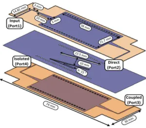
The geometry of the double-layered SIW coupler consists of two SIWs – one on top of the other coupled through two slanted slots as shown in Fig. 3. The length, the angle and the distance of the 1 mm thick slanted slots are optimized to achieve maximum coupling level at the operation frequency of 5.8 GHz [4]. Two 254 µ m thick polyimide films are stacked which results in an overall coupler size of 30 mm 74 mm with total thickness of 0.5 mm. The volume of the proposed coupler (0.74 0 0.42 0 0.01 0) in multilayer SIW
configuration was successfully miniaturized by about 58 times in terms of wavelength at the operation frequency compared to a previously reported coupler (2 0 1 0 0.09 0) [4]. The two
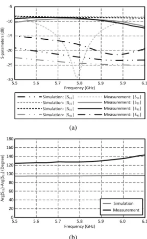
individual SIWs have been printed separately on the two overlying polyimide layers that share a ground plane which has the slanted slot for coupling. The proposed coupler has utilized the same fabrication and design method with the flexible inkjet-printed SIW interconnect. The coupler has been designed and optimized for the operation frequency at 5.8 GHz with a 90 degree phase difference between the coupled (Port3) and the direct port (Port2) [5]. The measured 4-port
S-parameters and the phase difference are shown in Fig. 4. The measured insertion loss of the fabricated multilayer coupler is 9.3 dB and the phase difference is 127 degrees at 5.8 GHz as shown in Fig. 4, while the simulated insertion loss and phase difference are 8.5 dB and 96.7 degrees, respectively. The fabricated coupler has relatively broad bandwidth of 10.3 %. Additional losses from the conductors have occurred due to the fact that the measured thickness of the printed conductive lines is about 2.4 µ m while the skin depth of the printed silver nanoparticle layer at 5.8 GHz is about 2.7 µm.
III. PRINTED MULTILAYER COUPLER FABRICATION
The inkjet-printed SIW-based interconnect and broadband coupler proposed in this work are constructed in three steps. The first step involves the cutting of the 254 µm thick substrate along the outline of the design using a laser cutter. Cutting the 254 µm thick polyimide film uses Epilog system's Legend 36EXT with a laser power of 7.2 Watts in a scanning speed of 5.0 cm/s and a resolution of 1200 pulse per inch (PPI). The laser cut substrate is thoroughly washed in flowing water to wash away the blackening and dust.
Step two is to focus on the inkjet printing of the SIW and ground patterns on the prepared substrate. The substrate surface is cleaned using 99% ethanol. A Dimatix DMP-2800 printer is used to print Advanced Nano Products' DGP 40LT-15C silver nanoparticle ink. A 10 pL cartridge is utilized in a nozzle temperature of 37.5 °C and a printer's platen temperature of 60 °C with a drop spacing of 30 µ m (847 dpi) in order to prevent running of the printed ink on the polyimide film. A higher platen temperature is desirable to dry the printed silver nanoparticle as fast as possible and optimized drop spacing is required to balance the surface energy of the substrate and the surface tension of the printed ink. The ground plane with the slanted slots is printed on one side and the SIW patterns are printed on the other side of the two layers. Each pattern is printed three times. Solid patterns (without via holes) are printed over the via holes in order to form a
(a)
(b)
Fig. 1. (a) Schematic of the designed SIW interconnect. (b) Simulated and measured the microstrip-to-SIW transitions and 20 mm long SIW.
Fig. 2. Flexibility test of the fabricated SIW interconnect.
continuous ink layer on the via holes. The via holes were successfully metalized by printing over the via holes 3 times on each layer. The measured resistance of the 254 m long inkjet-printed via was about 2.4 ~ 2.7 Ω. The printed pattern is dried at 100 °C for 30 mins and the pattern for the other layer is printed. The alignment function of the printer is utilized to align the printing point which has a 20 µm mechanical error. The printed prototypes are cured at 130 °C for 1 hour as a last step of printing. The measured thickness of every individual inkjet-printed conductive layer with 30 µ m drop spacing is about 800 nm and the conductivity value of the cured silver nanoparticle layer is about 6 106 S/m.
The final step is the alignment and the bonding of the printed layers. Two wires with a diameter that fits the via hole dimensions are inserted in two via holes at opposite via walls to align the top and bottom layer. The via holes are filled by a conductive epoxy to maintain the alignment and firm contact of the two layers.
IV. SUMMARY &FUTURE WORK
A flexible SIW interconnect and a compact multilayer broadband coupler utilizing the inkjet printing fabrication method have been demonstrated for the first time. The inkjet-printed SIW interconnect and multilayer compact coupler
successfully demonstrated the feasibility of flexible 2D/3D SIW systems utilizing inkjet printing technology. The multilayer coupler is a first step toward the inkjet-printed multilayer electronics systems for wearable, sensing, RFID and communication systems. An inkjet-printed compact multilayer Butler matrix for sensing, RFID and communication applications like a multibeam antenna (MBA) system can be built based on the study presented in this paper. The relatively high loss can be improved by increasing the metal thickness by printing more layers and using low loss flexible substrates, such BCB and LCP [6]. The conductor loss can be further reduced by increasing the substrate thickness [3,7].
ACKNOWLEDGEMENT
This work was supported by support of National Science Foundation (NSF).
REFERENCES
[1] A. Nathan, A. Ahnood, M. T. Cole, S. Lee, Y. Suzuki, P. Hiralal, F. Bonaccorso, T. Hasan, L. Garcia-Gancedo, A. Dyadyusha, S. Haque, P. Andrew, S. Hofmann, J. Moultrie, C. Daping, A. J. Flewitt, A. C. Ferrari, M. J. Kelly, J. Robertson, G. Amaratunga and W. I. Milne, " Flexible Electronics: The Next Ubiquitous Platform," Proc. IEEE, vol.100, pp.1486-1517, May 2012.
[2] M. Bozzi, A. Georgiadis and K. Wu, "Review of Substrate-Integrated Waveguide Circuits and Antennas," IET Microw.
Antennas Propag., vol.5, no.8, pp.909-920, June 2011.
[3] D. Deslandes and K. Wu, "Integrated Microstrip and Rectangular Waveguide in Planar Form," IEEE Microw. Wireless Compon.
Lett., vol.11, no.3, pp.68-70, Feb. 2001.
[4] J. -X. Chen, W. Hong, Z. -C. Haom H. Li and K. Wu, "Development of a Low Cost Microwave Mixer using a Broad-band Substrate Integrated Waveguide (SIW) Coupler," IEEE
Microw. Wireless Compon. Lett., vol.16, no.2, pp.84-86, Feb.
2006.
[5] A. A. M. Ali, N. J. G. Fonseca, F. Coccetti and H. Aubert, "Design and Implementation of Two-Layer Compact Wideband Butler Matrices in SIW Technology for Ku-Band Applications,"
IEEE Antennas Propag. Mag., vol.59, no.2, pp.503-512, Jan.
2010.
[6] H. Sharifi, R. R. Lahiji, H. -C. Lin, P. D. Ye, L. P. B. Katahi and S. Mohammadi, "Characterization of Parylene-N as Flexible Substrate and Passivation Layer for Microwave and Millimeter-(a)
(b)
Fig. 4. (a) S-parameters of the inkjet-printed multilayer coupler and (b) phase difference between the direct (Port2) and the coupled port (Port2)
(a) (b)
Fig. 5. Inkjet-printed multilayer broadband coupler on polyimide film: (a) SIW layer for top and bottom layer (b) ground plane with two slanted slots.
Wave Integrated Circuits," IEEE Trans. Adv. Packag., vol.32, no.1, Feb. 2009.
[7] R. Moro, S. Kim, M. Bozzi and M. M. Tentzeris, "Inkjet-Printed
Paper-Based Substrate Integrated Waveguide (SIW)
Components and Antennas," Int. J. Microw. Wireless Tech., vol.5, no.3, May 2013.