HAL Id: hal-03095123
https://hal.laas.fr/hal-03095123
Submitted on 4 Jan 2021
HAL is a multi-disciplinary open access
archive for the deposit and dissemination of
sci-entific research documents, whether they are
pub-lished or not. The documents may come from
teaching and research institutions in France or
abroad, or from public or private research centers.
L’archive ouverte pluridisciplinaire HAL, est
destinée au dépôt et à la diffusion de documents
scientifiques de niveau recherche, publiés ou non,
émanant des établissements d’enseignement et de
recherche français ou étrangers, des laboratoires
publics ou privés.
Implant heating contribution to amorphous layer
formation: a KMC approach
P.L. Julliard, P. Dumas, F. Monsieur, F. Hilario, D. Rideau, Anne Hémeryck,
Fuccio Cristiano
To cite this version:
P.L. Julliard, P. Dumas, F. Monsieur, F. Hilario, D. Rideau, et al.. Implant heating contribution
to amorphous layer formation: a KMC approach. 2020 International Conference on Simulation of
Semiconductor Processes and Devices (SISPAD), Sep 2020, Kobe, Japan. pp.43-46,
�10.23919/SIS-PAD49475.2020.9241608�. �hal-03095123�
XXX-X-XXXX-XXXX-X/XX/$XX.00 ©20XX IEEE
Implant heating contribution to amorphous layer
formation: a KMC approach
P.L. Julliard*1,2, P. Dumas1, F. Monsieur1, F. Hilario1, D. Rideau1, A. Hemeryck2, F. Cristiano2 1ST Microelectronics, Crolles, France
2LAAS-CNRS, Université de Toulouse, CNRS, Toulouse, France
Email: [email protected]
Abstract—The present work investigates the influence of
implantation induced heating on the amorphization profile in silicon wafer. A simulation approach based on a Kinetic Monte Carlo method is compared to experimental implantations and characterizations. We demonstrate that a backside pressure cooling can be used to tune amorphous layer thickness.
Keywords—amorphization, Kinetic Monte Carlo, implantation induced heating, machine parameters
I. INTRODUCTION
Ion implantation is a widely used process in the semi-conductor industry to introduce dopants into silicon substrates and leads to amorphization under specific conditions. While amorphous silicon recrystallizes upon annealing, excess self-interstitials lying in crystalline areas evolve in extended defects such as {311} or dislocation loops [1]. Extended defects are known to induce several issues in semiconductor devices. The first one is the degradation of electronic performances as dislocation loops can induced leakage current in transistor [2]. Extended defects also act as recombination or emission center for electron-hole pair and are involved in the degradation of optical properties [3]. Dark current in images sensors has been associated in some cases with the presence of dislocations [4]. Furthermore, extended defects can dissolve during the annealing. The dissolution of a dislocation or a {311} is followed by an increase of the supersaturation of interstitials. This increase of interstitials produced a well-known phenomenon: the transient enhanced diffusion (TED). Dopant diffusion can increase by a factor 100 or more during the first instant of the annealing and lead to a spreading of the dopants distribution [5].
A knowledge of the formation kinetic is necessary to control the presence of extended defects. The growth kinetics of such defects is not only driven by the annealing temperature but also by their position relative to the surface [6]. Therefore, the spatial distribution of both amorphous/crystalline areas after ion implantation is a key parameter for process optimization. Process optimization can be improved using Technology Computer-Aided Design (TCAD). Reliable TCAD simulations therefore need complete and accurate models for implantation induced amorphization [7].
Amorphization is a complex phenomenon involving several parameters such as the ion dose, the wafer temperature, the mass of the implanted ion and the frequency between ions collisions (dose rate) [8]. Certain parameters driving amorphization are themselves dependent on the machine parameters used for implantation. The dopants are implanted by the mean of a beam sending ions on a delimited area on the wafer. The part of the wafer exposed to the beam changes with time to obtain a uniformly implanted wafer. A given area on the wafer is therefore alternatively heated and cooled down, depending if it is exposed to the beam or not.
Industrial implanters include a cooling system that, notably, prevents the resist from being damaged during implantation [9]. However, despite the cooling system, the ion beam heats up the wafer, which could impact the amorphization dynamic. In most cases, the temperature increase can be relatively modest, which has no impact on amorphization [10]. However, this work focuses on implantations with higher beam energy than in [10] which could lead to a greater heating. Machine parameters are essential in the heating phenomenon and therefore for the amorphization phenomenon. This work investigates the impact of backside cooling pressure on amorphization comparing experimental data and Kinetic Monte Carlo (KMC) simulations.
II. EXPERIMENTAL AND SIMULATION METHOD
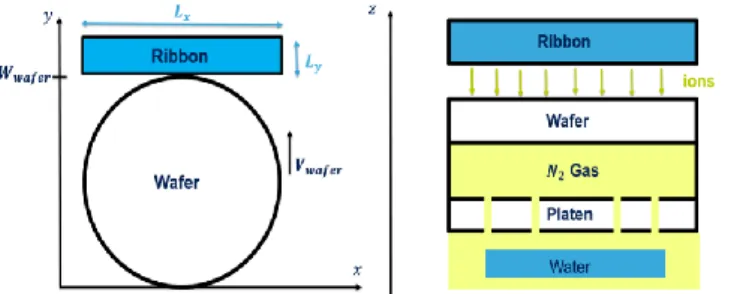
The implanter used here is an industrial Viista HCS implanter supplied by Applied Material. Its end-station configuration is presented in Fig. 1. A fixed ribbon beam sends ions with a constant flux on the wafer which moves back and forth face to the ribbon beam. An implantation is divided into 𝑁𝑝𝑎𝑠𝑠𝑒𝑠 back
and forth on the wafer to reach the total dose. Incidents ions hit the wafer with an energy 𝐸𝑖𝑜𝑛𝑠. The ions flux is given by
the current 𝐼𝑏𝑒𝑎𝑚. The first step of this work is to simulate the
temperature profile during implantation depending on machine parameters. The temperature is calculated for one given wafer sub-area at the wafer center. For this given area, the heat equation is separated in two parts: a heating phase when the beam irradiates the area and a cooling phase when the beam is located elsewhere on the wafer. In equation (1), 𝑝𝑏𝑒𝑎𝑚 is the power induced per unit area (
𝐸𝑖𝑜𝑛𝑠∗𝐼𝑏𝑒𝑎𝑚 𝑞𝐴 with 𝑞
the Coulomb constant and 𝐴 the surface of the implanted area) 𝜌𝑐𝑝
𝑑𝑇
𝑑𝑡 = −𝛼𝑝𝑐𝑜𝑜𝑙𝑖𝑛𝑔(𝑇 − 𝑇𝑓) + 𝑝𝑏𝑒𝑎𝑚(𝑡) ()
𝜌 and 𝑐𝑝 are the silicon mass density and thermal
capacitance. 𝑇𝑓 is the water temperature (see Fig. 1). 𝛼 is an
surface roughness constant and 𝑝𝑐𝑜𝑜𝑙𝑖𝑛𝑔 is the cooling gas
pressure.
Fig. 1: Scheme of the implanter end-station used in this work (left) and of its cooling system (right).
This equation assumes an instantaneous diffusion of the heat along the depth of the wafer. The temperature profile is composed of 𝑁𝑝𝑎𝑠𝑠𝑒𝑠 cycles of heating-cooling, each pass
starting at the temperature reached at the previous one. The beam exposition time and the time between two successive beam expositions for the considered sub area are directly function of the machine parameters used during the implantation. These parameters can be evaluated during the implantation by machine sensors and are extracted to obtain the real dynamic of the implantation. The beam exposition time 𝑡𝑒𝑥𝑝𝑜𝑠𝑒𝑑 and the time between two passes on the center
of the wafer 𝑡𝑐𝑜𝑜𝑙𝑖𝑛𝑔 are calculated with the following
formulas: 𝑡𝑒𝑥𝑝𝑜𝑠𝑒𝑑 = 𝐿𝑥 𝑉𝑤𝑎𝑓𝑒𝑟 (2) and 𝑡𝑐𝑜𝑜𝑙𝑖𝑛𝑔= 𝑊−𝐿𝑥 𝑉𝑤𝑎𝑓𝑒𝑟 (3)
Parameters such as the currents used during implantation or the number of passes are also extracted from the equipment sensors.
The temperature trend with time is a saw-tooth like increase. The temperature profile is coupled to the input files of Sentaurus KMC software [11] to model implantation at the calculated temperatures. The total implantation is subdivided in 𝑁𝑝𝑎𝑠𝑠𝑒𝑠 implantations and 𝑁𝑝𝑎𝑠𝑠𝑒𝑠 cooling times between
implantations in the input files of Sentaurus. Each sub implantation is simulated at the corresponding temperature. Time between implantations allows diffusion and recombination of defects.
Sentaurus KMC calculates each point defect but also enables to plot average 1-D profiles along the depth of the wafer. When the concentration of point defects overcomes 1.5 1022 𝑐𝑚−3 in a region, it is considered as amorphous.
This enables amorphization 1-D profiles along the depth of the wafer.
In the presented method to calculate wafer heating, different cooling gas pressures lead to different local temperature increases of the wafer. A solution to highlight temperature contribution is to simulate the same implantation with different cooling pressures. Fig. 2 shows the simulation of temperature for a 60 keV carbon ion implantation with a dose of 1.5 1015𝑐𝑚−2 at three different backside cooling pressures
(4, 9 and 15 Torr). Fig. 2 highlights that the smaller the cooling pressure, the higher the wafer heating, in agreement with equation (1).
Fig. 2: Simulation of temperature evolution during a 60 keV carbon implant with a dose of 1.5 1015𝑐𝑚−2 for three different cooling pressures (4, 9 and
15 Torr).
III. RESULTS AND DISCUSSION
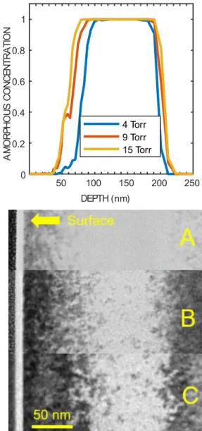
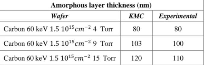
The amorphization generated by the previously mentioned 60 keV carbon implantations is simulated with Sentaurus KMC coupled with the generated time dependent temperature profile. The amorphous layer is defined by the depth where the concentration of point defects is above the amorphization threshold value. The results demonstrate that the amorphous layer thickness increases with the cooling pressure used during implantation (Fig. 3). The amorphous layer thickness for a 4 Torr cooling pressure only reaches 90 nm as compared to the 120 nm amorphous thickness obtained at 15 Torr. This result can be compared to the amorphous layer thickness measured by transmission electron microscopy (TEM) images given on Fig. 3. Estimation for amorphous thickness could be extracted by plotting the laterally integrated contrast versus depth of the TEM images. Silicon is considered amorphous when its brightness is at 85 percent of the brightest point. Simulation and experimental results for these implantations are summarized in Table I.
Fig. 3: (Top) Simulation of amorphous concentration as function of the depth for a 60 keV carbon implantation with a dose of 1.5 1015 𝑐𝑚−2 and for
cooling pressures of 15, 9 and 4 Torr. (Bottom) A, B and C are the TEM images of 60 keV carbon implanted wafers with a dose of 1.5 1015 𝑐𝑚−2
and a cooling pressure of 15, 9 and 4 Torr respectively.
The effect of the cooling pressure on amorphization for a 30 keV carbon implantation at a dose of 2 1015𝑐𝑚−2 and cooling
pressures of 4 and 9 Torr is also simulated in this work. The difference in temperature for the two implantation conditions can be observed in Fig. 4. The effect of the pressure is the same as for the 60 keV implantation. A smaller cooling pressure induced higher temperature during implantation. Amorphization profile for these two conditions is simulated in Fig. 5. The difference of simulated amorphization is much smaller but follows the same trend as the 60 keV carbon implantation. The higher the cooling pressure, the thicker the amorphous layer. TEM images of these 30 keV implantations show more crystalline areas near the surface for the high-pressure case (Fig. 4). This confirms that amorphization tends to increase with cooling pressure.
Fig. 4: Simulation of temperature evolution during a 30 keV carbon implant with a dose of 2 1015𝑐𝑚−2 for two different coolingpressures (4, 9 Torr).
This trend is particularly highlighted by the ion and the dose investigated in the two previous experiments. The dose of 1.5 1015 𝑐𝑚−2 is close to the amorphization threshold dose
𝐷𝑐𝑟𝑖𝑡𝑖𝑐𝑎𝑙 for carbon at room temperature. The more the
implanted dose is superior to the threshold dose value, the less the effect of cooling pressure on amorphization is observed. For an implanted dose of 4 1015 𝑐𝑚−2 and for cooling
pressures of 4, 9 and 15 Torr, the difference in temperature is still observed and even more present than in the previous 2 1015 𝑐𝑚−2 implantation (see Fig. 6). The difference in
amorphization is not observed in TEM images. The KMC simulation does not predict difference in amoprhization for these temperature differences (Fig. 7). Simulation and experiment are consistent and show a diminution of the effect when the dose increases.
Fig. 5: (Left) Simulation of amorphous concentration as function of the depth for a 30 keV carbon implantation with a dose of 2 1015 𝑐𝑚−2 and for cooling
pressures of 9 and 4 Torr. (Right) A and B are the TEM images of 30 keV carbon implanted wafers with a dose of 2 1015 𝑐𝑚−2 and a cooling pressure
of 9 and 4 Torr respectively.
Fig. 6: Simulation of temperature evolution during a 30 keV carbon implant with a dose of 2 1015𝑐𝑚−2 for two different coolingpressures (4, 9 Torr).
Fig. 7: (Top) Simulation of amorphous concentration as function of the depth for a 30 keV carbon implantation with a dose of 4 1015 𝑐𝑚−2 and for cooling
pressures of 4, 9 and 15 Torr. (Bottom) A, B and C are the TEM images of 30 keV carbon implanted wafers with a dose of 4 1015 𝑐𝑚−2 and a cooling
pressure of 15, 9 and 4 Torr respectively.
This phenomenon is linked with the dynamic of growth of an amorphous layer. The growth of an amorphous layer is the consequence of damages accumulation in silicon. The damages accumulation regarding the implanted dose is composed in three distinct regimes for a light ion implantation (see Fig. 8). The first regime is a sublinear growth of the damages in silicon until small amorphous areas are formed. For higher implanted doses the defects growth follows a superlinear behavior where silicon is composed of both crystalline and amorphous areas. The third regime is a platen corresponding to the creation of an amorphous layer and is reached when the dose overcomes a value 𝐷𝑐𝑟𝑖𝑡𝑖𝑐𝑎𝑙. The
damages profile is not uniform along the depth of the implanted wafer. When the critical dose is reached, the amorphous layer is formed at the depth where damages are maximum. If the implanted dose overcomes 𝐷𝑐𝑟𝑖𝑡𝑖𝑐𝑎𝑙 ,
damages are still increasing in non-amorphous areas. The amorphous layer expends in the neighboring regions where the damages accumulated are close to the amorphization threshold for a 𝐷𝑐𝑟𝑖𝑡𝑖𝑐𝑎𝑙 implanted dose. The expansion of the
amorphous layer with dose stops when all damaged regions are amorphous. This explains the constant amorphous layer thickness in Fig. 7. The dose is high enough to amorphize along all the damages profile for all temperature conditions. For 1.5 1015 𝑐𝑚−2 implantation, region between the surface
and the amorphous layer are in the superlinear behavior and a small change in implantation parameters induces a visible difference in amorphization profile.
Fig. 8: Superlinear behavior of the damage vs dose for a 230 keV Si implant into S (100) at room temperature reproduced from [8]. Symbols represent the maximum defect concentration as extracted from channeling spectra.
The superlinear behavior is also an effect correlated with the mass of the implanted ion. The lighter the implanted ion specie, the sharper the superlinear slope [12]. Heavy species ions do not demonstrate strong super-linear behavior compared to carbon. Heating during implantation is therefore expected to be more relevant for light ion species.
TABLE I. COMPARAISON BETWEEN SIMULATION AND EXPERIMENTAL DATA FOR AMORPHOUS LAYER THICKNESS
Amorphous layer thickness (nm)
Wafer KMC Experimental
Carbon 60 keV 1.5 1015𝑐𝑚−2 4 Torr 80 80
Carbon 60 keV 1.5 1015𝑐𝑚−2 9 Torr 103 100
Carbon 60 keV 1.5 1015𝑐𝑚−2 15 Torr 120 110
IV. CONCLUSION
KMC simulations and experimental data are consistent and showed that amorphous thickness can be tuned from dozen of nm to less than 5 nm by changing backside pressure cooling on a standard industrial implanter. The impact of the backside cooling pressure is more relevant when the implanted dose approaches the threshold value of amorphous layer formation. This behavior is also predicted by KMC simulations.
V. REFERENCES
[1] C. Bonafos, D. Mathiot and A. Claverie. "Ostwald ripening of end-of-range defects in silicon." Journal of Applied Physics, vol. 83, no. 6, pp. 3008-3017. (1998).
[2] C. Nyamhere, A. Scheinemann, A. Schenk, A. Olivie, F. Cristiano . "A comprehensive study of the impact of dislocation loops on leakage currents in Si shallow junction devices. " Journal of Applied Physics, vol. 118, no 18, pp. 184501.(2015)
[3] Y. Wei et al. "Analysis of dark current dependent upon threading dislocations in Ge/Si heterojunction photodetectors." Microelectronics international (2012).
[4] T. Hoang, J. Holleman, P. Leminh et al. "Influence of dislocation loops on the near-infrared light emission from silicon diodes." IEEE transactions on electron devices, vol. 54, no 8, pp. 1860-1866.(2007).
[5] S.C. Jain, W. Schoenmaker, R. Lindsay et al. "Transient enhanced diffusion of boron in Si. " Journal of applied physics, vol. 91, no 11, p. 8919-8941.( 2002).
[6] B. Colombeau, N.E.B Cowern, F. Cristiano, P. Calvo, N. Cherkashin, Y. Lamrani and A. Claverie. "Time evolution of the depth profile of {113} defects during transient enhanced diffusion in silicon." Applied physics letters, vol. 83, no. 10,pp. 1953-1955. (2003).
[7] N. Zographos, and I. Martin-Bragado "A Comprehensive Atomistic Kinetic Monte Carlo Model for Amorphization/Recrystallization and its Effects on Dopants" Mater. Res. Soc. Symp. Proc. vol. 1070, (2008). [8] L. Pelaz, LA. Marqués, and J. Barbolla. "Ion-beam-induced amorphization and recrystallization in silicon." Journal of applied physics,vol. 96, no.11, pp. 5947-5976.(2004).
[9] T. C.Smith, "Wafer cooling and photoresist masking problems." Ion Implantation: Equipment and Techniques: Proceedings of the Fourth International Conference Berchtesgaden, Fed. Rep. of Germany, September 13–17, 1982. vol. 11. Springer Science and Business Media, (2012).
[10] HJ. Gossmann, N. Zographos et al. "Predictive process simulation of cryogenic implants for leading edge transistor design." AIP Conference Proceedings. vol. 1496., no. 1. American Institute of Physics, (2012). [11] Sentaurus Process User Guide, 2019.03, Synopsys Inc.
[12] E. C. Baranova., V. M. Gusev, Y.V. Martynenko et al. "On Silicon Amorphisation During Different Mass Ions Implantation. " Ion implantation in semiconductors and other materials. Springer, Boston, MA, p. 59-71.(1973).