Cavity-Assisted All-Optical Photodetection
by
Christopher Louis Panuski
B.S.
in Electrical Engineering
B.S. in Physics
United States Naval Academy, 2017
MAsSACHUSETTS WTT f
OF TECHNOLOGY
JUN 13
0119
LIBRARIES
ARCHIVES
Submitted to the Department of Electrical Engineering and Computer
Science
in partial fulfillment of the requirements for the degree of
Master of Science in Electrical Engineering and Computer Science
at the
MASSACHUSETTS INSTITUTE OF TECHNOLOGY
June 2019
@
Massachusetts Institute of Technology 2019.
Author ...
All rights reserved.
Signature redacted
Department of Electrical Engineering and Computer Science
May 23, 2019
Certified by ...
Signature redacted
Dirk R. Englund
Associate Professor of Electrical Engineering and Computer Science
Thesis Supervisor
Accepted by...Signatue
edacted
/
U&
Leslie A. KolodziejskiProfessor of Electrical Engineering and Computer Science
Chair, Department Committee on Graduate Students
Cavity-Assisted All-Optical Photodetection by
Christopher Louis Panuski
Submitted to the Department of Electrical Engineering and Computer Science on May 23, 2019, in partial fulfillment of the
requirements for the degree of
Master of Science in Electrical Engineering and Computer Science
Abstract
The free-carrier dispersion effect - which is resonantly enhanced by a cavity's quality factor to mode volume ratio Q/Veff - enables ultrafast, energy-efficient, all-optical control of semi-conductor resonators. When applied to recently developed photonic crystal cavities with record-high Q/Veff values, this enhanced light-matter interaction unveils new possibilities in nonlinear optics. Here, by considering the free-carrier dispersion effect at the limit of a single photoexcited charge carrier pair, we analyze the possibility of realizing room-temperature, all-optical single photon detection.
Thesis Supervisor: Dirk R. Englund
Acknowledgments
Over the past two years, I have had the joy of working with an experienced, ambitious team of researchers in Professor Dirk Englund's Quantum Photonics Group (QPG). Professor Englund readily welcomed me to this team, trusted me to study his proposals, and supported several of my own. His leadership, creativity, and enthusiasm made this current endeavor possible; I look forward to continuing to grow as a doctoral student under his guidance.
I would also like to specifically thank the coauthors of this project - Mihir Pant, Mikkel
Heuck, and Ryan Hammerly. Mihir's mentorship kept my research on track and significantly improved my tennis skills. Mikkel, our resident Dane, assisted with the computational aspects of the project and informed us of Denmark's beauty daily. Ryan's genius pushed me to introduce more mathematical rigor into my research. Ever since he validated my months of simulations with less than a day of theory work, I've always thought twice about looking for analytic solutions.
Outside of this small team, the broader QPG community has made my experience at MIT an enjoyable one. I was lucky enough to have two incredible officemates Mihika Prabhu arid Cheng Peng who were always happy to discuss new ideas "early" in the morning. Jacques Carolan kept the group up-to-date on the hipster community's latest coffee trends, Darius Bunandar and Ben Lienhard ensured no complaint was left unvoiced, Michael Walsh's IT support arid sounding board was always a short walk away, and Eric Bersin went to Harvard. Without the support of the Hertz Foundation community, I would not have been able to pursue my dream of studying here at MIT. In addition to their gracious funding (specifically provided by the Elizabeth and Stephen Fantone Family; thank you!), the Foundation was key in helping to coordinate my graduate studies with the Navy. The community's unwavering trust has also given me the confidence to propose arid explore independent research directions beyond my group's primary efforts.
Outside of the lab, I was blessed to have an incredible group of friends -- Josh Perozek, Matt Johnson, Jamie Hood, and Wes Hill - who brought me along on their outdoor adven-tures. Finally, I am indebted to my loving mother, father, and two brothers, Patrick and Benjamin - you guys make it easy to wake up excited everyday!
Contents
1 Introduction 9
1.1 All-Optical Photodetection . . . . 9
1.2 Enabling Technology - High-Q/V Photonic Crystal Cavities . . . . 10
1.3 O rganization . . . . 11
2 Free Carrier Dispersion 13 2.0.1 Method I: Drude Model . . . . 14
2.0.2 Method II: Empirical Model . . . . 14
2.0.3 Comparison . . . . 15
2.1 Free Carrier Absorption . . . . 15
2.2 Comparison to Other Nonlinearities . . . . 15
3 Optimized, Cavity-Assisted Architectures 19 3.1 Single Cavity Theory . . . . 19
3.1.1 Architecture and Performance Metrics . . . . 19
3.1.2 Optimization . . . . 22
3.2 Coupled Cavity Design . . . . 24
3.2.1 Architecture and Performance Metrics . . . . 25
3.2.2 Optimization . . . . 26
3.3 Jitter . . . . 26
3.4 Photon Number Resolution (PNR) . . . . 27
3.5 Sum m ary . . . . . 27
4 Dark Count Rates and Mode Volumes 31 4.1 Dark Count Contributions . . . . 31
4.1.1 Thermal Noise . . . . 31
4.1.2 Multiphoton Absorption . . . . 35
4.2 Dark Count Mode Volumes . . . . 36
4.2.1 D erivation . . . . 36
4.2.2 Scaling Analysis . . . . 38
4.2.3 Numerical Evaluation for PhC Cavities . . . .. 42
4.3 Optimization . . . . 44
5 Absorption 47
5.1 FDTD Simulations ... ... 47
Chapter 1
Introduction
1.1
All-Optical Photodetection
Despite the central importance of photodetection for a variety of applications ranging from biomedical imaging, to lidar and optical communications, photodetectors are commonly the performance limiting component in both classical and quantum optical technologies. Specifi-cally, a single photon detector that simultaneously excels in a variety of performance metrics
-including high count rate, low timing jitter, low dark count rate, photon-number-resolution, and low power consumption - is still an outstanding goal, in part due to the limitations imposed by the dependence of the photodetector upon electronic transduction and amplifi-cation. For example, traditional semiconductor-based single-photon detectors, such as the popular silicon avalanche photodiode (APD), rely on three basic mechanisms: (1) an atomic excitation, such as the generation of free charge carrier pairs, induced by the absorption of a signal photon; (2) the amplification of this excitation through an electronic avalanche process; and (3) the thresholding, sampling, and analog-to-digital conversion of the resulting signal using electronic equipment. Single photon APDs have been developed in a range of materials and platforms [1, 2], but their performance remains limited by the need to con-currently design optical absorption and electrical readout mechanisms. Jitter performance is limited by factors including the inhomogeneous travel time of carriers across the junction, and the limited electrical readout bandwidth. Electronic defects in the amplification region contribute to false detection events, a phenomena which is particularly significant in non-Si APDs. Despite decades of development of passive and active reset mechanisms, reset times are also still long - typically tens to hundreds of nanoseconds [1]. Alternatively, supercon-ducting single photon detectors enable high detection efficiency, low dark count rates, and few-ps jitter, but require cryogenic cooling and have limited count rates due to their long dead times [3-5].
These examples of state-of-the-art photodetectors illustrate the limitations inherent to amplification in the electronic domain: high thermal noise as well as slow carrier and am-plifier response times. Here, we propose a new class of room temperature semiconductor photodetectors that addresses these limitations by realizing single photon amplification in the optical domain. This readout technique retains the benefits of an optical channel: neg-ligible thermal noise, large bandwidth, and low-loss transmission.
a) Signal Photon
Probe Beam
-
U~
** Semiconductor Probe Output
b) c)
i'
- (Ann)free carrier Q r i E,> E9'VVIiEj
E~E9 9 .. >. Ep < E -FRequency, wFigure 1-1: Ultrafast all-optical detection of single photons. (a) A signal photon is absorbed in a photonic
nanocavity, leading to the generation of a photo-excited charge carrier pair within a "hot spot" volume Vhot.
(b) A sub-bandgap optical probe interrogates the cavity, and is phase shifted as a result of the resonance
shift (c) produced by the presence of the additional free carrier.
Fig. 1-1(a) illustrates the concept. The absorption of a signal photon in a semiconduc-tor optical cavity excites a free electron-hole charge carrier pair (Fig. 1-1(b)), which nearly instantaneously shifts the solid-state medium's refractive index - and in turn the cavity's resonant frequency - through the free carrier dispersion effect (Fig. 1(c)). If interrogated with a sub-bandgap probe, the resulting change in resonant frequency imparts a phase shift on the transmitted light that can be detected using heterodyne or homodyne detection with common high-speed p-i-n photodetectors [6-8], which need not be single-photon resolving. This process constitutes all-optical gain, as the change in cavity transmission induced by a single signal photon can be converted into a strong probe signal at the homodyne receiver. Since the output signal remains in the optical regime, it can be directly used to run modula-tors or other optical components within the system without requiring electronic processing, thus circumventing a traditional bottleneck of optical computing.
If experimentally feasible, the realization of a room temperature single photon detection
enabled by all-optical amplification would immediately impact a range of quantum optical technologies, and could even enable entirely new applications. To this end, we analyze the performance achievable by a cavity-based all-optical photodetector, and determine the experimental requirements for efficient single photon detection.
1.2
Enabling Technology
-
High-Q/V Photonic Crystal
Cavities
The all-optical scheme analyzed in this thesis was motivated by recent experimental and the-oretical developments in photonic crystal (PhC) technology. A simple back-of-the-envelope calculation shows that the sensitivity of the cavity-based detector is proportional to the cav-ity's quality factor to mode volume ratio Q/Ve, where Q = wo/F for a resonance frequency
wo and energy decay rate F, and Veff is the mode volume defined in Chapter 2 for point-like
perturbations. Within the past few years, fabrication advances have improved experimental quality factors to ~107 in diffraction-limited [Ve ~ (A/n)3 for a wavelength A and sub-strate index of refraction n] silicon PhC cavities [9, 101. In parallel, clever dielectric designs were proposed [11, 12] to enable deep-subwavelength mode volumes [Vff < (A/n)3]. Previ-ous proposals had shown [13] that introducing subwavelength slots into dielectric structures could shrink Vff as a result of the boundary condition for a continuous normal component of electric displacement D = eE. The more recent "tip-based" designs simply extend this boundary condition-based intensity enhancement to a structure that simultaneously reduces mode volume through the parallel boundary condition for the electric field E. Fabricated devices
[14]
with Vef ~ -3(A/r 3 andQ
~ 10' have validated this technique within the last year.The ability to achieve Q/Veff ratios on the order of 10' unveils exciting opportunities in nonlinear optics and sensing. For the latter, an index perturbation of An/n ~ 10- could in principle lead to a linewidth-order resonance shift. This consideration motivated our study to answer a simple question: could the absorption of a single photon be detected in the transmission of a high-Q/Vff PhC cavity?
The readout architectures we analyze are abstracted from any particular cavity design, and are therefore valid for any semiconductor cavity. However, some performance metrics -such as the dark count rate depend on the shape of the optical mode within the cavity. We analyzed the mode profiles of both traditional diffraction-limited and ultrasmall mode volume cavities to quantify these metrics, and surprisingly found that the ultrasmall mode
volume cavities suppress higher-order nonlinear noise processes.
1.3
Organization
The remainder of this thesis is organized as follows. In Chapter 2, we analyze the effect of single photo-excited charge carrier pairs in an optical cavity and compare the result to other nonlinear effects. This cavity response is optimized for two ideal architectures in Chapter 3 before considering various noise sources in Chapter 4. The absorption efficiency of single photons in then briefly considered in Chapter 5. Chapter 6 summarizes the work and considers possible enhancements to the all-optical photodetection scheme. The content is derived from our published analysis [15].
Chapter 2
Free Carrier Dispersion
Suppose that a single photon is absorbed at the center of a cavity as shown in Fig. 1-1(a). Free carrier dispersion from the photo-excited free electron-hole pair yields a complex per-mitivity shift AE that, according to first order perturbation theory [16], induces a fractional resonance shift
AW I f da rg E~g A- ~ f -- ~ E~) (2.1)
wo 2 f da ;()IE(f)12
due to the permittivity shift Ae(f) within the electric field profile E(iF). In accordance with the Drude model, we assume that the fractional index change An/n ~ AE/2E is directly proportional to the free carrier density. For a uniform, perturbative index change within a small "hot spot" volume VhOt near the cavity's peak energy density at ' = Tmax, Eqn. 2.1
simplifies to
3- An() M (I9 2
Aw Jhtdrf(mxEfmax) An Vhot_7VQtx
- d r
~(2.2)
WO f dc(T|E()1 2 n Veff Vht Veff Veff'
max{IEE2 }
where we have defined -y as the constant of proportionality between An/n and carrier density (1/Vhot) and introduced the standard effective optical mode volume [17]
f d3 6 e(i)|IE(i;)|12
Veff = 2 (2.3)
max {e|E|2}
for point-like perturbations. Note that the validity of this analysis requires the absorption of the signal photon and the resulting index change to occur near the cavity's peak energy density (and thus well within the optical mode volume Vff).
Assuming complete mode confinement within the semiconductor, this result is identical to the frequency shift generated from a uniform carrier density 1/Veff throughout the mode volume. The resulting fractional resonance shift with respect to the linewidth F for a cavity with quality factor
Q
= wo/F isAW
Q
(2.4)
In other words, for any given -, a high Q/Veff ratio is desired. Silicon photonic crystal (PhC) cavities are therefore an ideal candidate, as recent fabrication advances have enabled cavities with intrinsic
Qs
of ~107 with Vff (A/n)3 [9, 10] and alternatively Qs of ~10' with modevolumes reaching ~10-3 (A/n)3 [14]. We now consider two ways to approximate Y in silicon.
2.0.1
Method I: Drude Model
Previous analyses have demonstrated that An is primarily a result of coulomb interactions with the free carrier, while Burstein-Moss bandfilling is negligible [18, 19]. Therefore, a simple Drude model analysis of this process estimates that the injection of a single free carrier pair into a volume Vhot will shift the complex permittivity c by
A~c= .W~t[~1T +_ T (2.5)
-jWe) m* (1 + jWTh)_
where qe is the electron charge, co is the vacuum permittivity, W is the probe frequency, and r and m* are the effective mass and mean collision time of the free charge carriers (electrons for "e" subscripts, and holes for "h" subscripts), respectively. The mean collision time governs the resulting behavior, and can be approximated using the experimentally measured mobilities [te ~ 1.5 x 103 cm2 V-1 s-1, IPh ~ 500 cm2 V- 1 s-' and effective masses mn* = 0.26me, m* = 0.39me of free carriers in undoped silicon at room temperature, which yields Te = Peme*/qe ~..' 0.22 ps and Th = /ihpm/qe ~ 0.11 ps [18, 20]. Assuming a probe wavelength of AO = 2.3 pLm is used to avoid two photon absorption (thus reducing the
detector dark count rate, as described in Chapter 4), the high-frequency limit Wr > 1 of Equation 2.5 for a weakly absorbing medium yields a frequency shift governed by
1 Ansi q 2 1 ii
2 V 2 -+ (2.6)
Vhot nsi 2n EOW2 T* Tn
and an additional free carrier absorption loss
Aa - 27r consiVht [TeM* + Thm*] L3. (2.7)
Ao q2
For a conservative estimate, we assume Vht = Veff for loss calculations. The results demon-strate that confining the free charge carrier pair within an experimentally-feasible probe optical mode volume Vff = 10-3(Ao/nsi) 3 = 2.8 x 10⁻⁴ pLm3 lends an overall index change of
Ansi ~ -1.5 x 10⁻⁵.
2.0.2
Method II: Empirical Model
Alternatively, -y can be approximated from the nonlinear empirical formula [18, 19]
Ansi = -p(A)[ne - cm3
]ql - r(A)[nh - cm3]s(A), (2.8)
where ne = 1/Vhot (nh) is the free electron (hole) density, and p, q, r', and s, are the wavelength (A) dependent coefficients tabulated in [19]. Eqn. 2.8 follows from absorption
measurements in silicon for wavelengths between 1.3 and 14 pm. Linearizing this model about Vff, we find ' ~ 1.1 x 10⁻⁸ (A/n)3 , a factor of -3 different from the previous
estimate.
2.0.3
Comparison
Both values indicate that a linewidth-order frequency shift requires a quality factor on the order of
Q
= Veff/1 ~ 10' for a probe optical mode volume Veff - 10-1 (Ao/nsi )3, oralternatively
Q
~0- for Veff 10-3 (Ao/nsi )3. As discussed in Chapter 3, optimization ofthe cavity architecture enables high signal-to-noise ratio (SNR) homodyne detection of the output probe signal with a fractional linewidth shift, even further reducing the necessary
Q.
The approach is therefore applicable to both standard diffraction-limited PhC cavities as well as state-of-the-art subwavelength-confined nanocavities [14J. Our subsequent analysis assumes an index change provided by Eqn. 2.8 due to the experimentally observed nonlinear scaling with respect to carrier density.Figure 2-1 provides an overview of the absorptive and dispersive effects of a single photon-induced free carrier nonlinearity as obtained from: 1) the Drude model estimate, and 2) extrapolation from the experimentally derived models in [18, 19].
2.1
Free Carrier Absorption
As mandated by the Kramers-Kronig relations, any index change induced by free carrier dispersion is accompanied by a corresponding loss: free carrier absorption (FCA). At a given resonant wavelength A, the associated absorptive quality factor
Qabs ~ wN (2.9)
2irnsi
is therefore of interest. Qabs can be estimated directly from experimental absorption data, or from the Drude model, where Qabs - w 3Tnsi/iW for a cavity resonance at w in a material with a plasma frequency wp = \//nq2/m6o -- resulting from the presence of a carrier density n of individual charge q, and mass m - and mean collision time T as determined by the carrier mobility. The results of Figure 2-1 illustrate that Qabs > 10' for all cavity mode volumes of interest [Veff 10-3 _ 1 (A/nsi)3]. Since we consider cavities with intrinsic quality factors
on the order of 105, we ignore this effect.
2.2
Comparison to Other Nonlinearities
Other rionlinearities, such as the optical Kerr effect, could be similarly enhanced within these
PhC cavities, as the maximum intra-cavity intensity scales with Q/Veff [21, 22]. However, free
carrier nonlinearities based on real transitions, while incoherent, are (generally) significantly stronger than those resulting from virtual transitions. The single photon Kerr nonlinearity,
10-4 10-6 1 10~1 .4 10-10 101 108 106
Free Carrier Nonlinear Effects in Si 2PA 3PA 4 A 5PA+
-- V-ff 10'(A/n)'
--- V = 102(A/n)3
V-ff = 103(A/n)3
FCD -Soref Data
FCD - Drude Model --- Single Photon Kerr 2PA 3PA 4 PA 5 5P A+
2 4 6
Wavelength A [pIm]
8 10
Figure 2-1: Dispersive and absorptive characteristics of the free carrier nonlinearity in the limit of a single photoexcited charge pair. The perturbation of the real component of the refractive index leads to a fractional frequency shift Aw/w a -Ansi/nsi, while free carrier absorption induces an additional loss Aa, corresponding to an absorptive quality factor Qabs f AaA/27rnsi. Both quantities can be estimated with the Drude model (dotted lines) or using the empirical models provided in [19]. Regardless of the approximation method, the strength is found to be much larger than that of a single photon Kerr nonlinearity (dashed).
for example, leads to a fractional resonance shift [12, 23]
WO Kerr
3x(3)(wo) Usig V2PA
4EOng Veff Veff (2.10)
for a third order nonlinear susceptibility X(3) and a signal photon energy Usig. The mode volume V2PA is defined in Chapter 4, and the ultrasmall mode volume cavity profile shown in Fig. 4-6 yields V2PA/Veff ~ 0.04. We estimate X (3)(w) using the mean fit provided in [24], which results in the values plotted in Figure 2-1 for a band-edge (Usig =1.1 eV) signal photon in silicon. The results illustrate that the effect is over an order of magnitude weaker than free carrier dispersion. The Kerr effect is also weaker at longer wavelengths, thus restricting the feasible range of probe wavelengths. Similar conclusions are provided in [18, 22], and we therefore focus on free carrier nonlinearities for the photodetection scheme.
absorbed signal photon produces a free electron-hole pair. Free carrier nonlinearities have previously enabled all-optical switching at GHz speeds with sub-femtojoule (~104 photons) switching energies [22]. While switching requires Aw F F, we show in Chapter 3 that photodetection can be achieved with Aw < F, which reduces the required input energy to the single photon level for recently developed high-Q/Veff PhC cavities.
Chapter 3
Optimized, Cavity-Assisted
Architectures
In this chapter, we analyze the two photodetection architectures shown in Fig. 3-1 using a temporal coupled mode theory approach [25-27].
Probe Beam
Sout T2
A-LO
Homodyne Detector (a) Single cavity readout.
Probe Beam
SotT2s
LO
Homodyne Detector
(b) Coupled cavity readout.
Figure 3-1: Single (a) and coupled (b) cavity architectures for all-optical single photon detection.
3.1
Single Cavity Theory
The simplest readout configuration consists of: 1) a single signal cavity, similar to that of Fig. 1-1, to amplify the phase shift generated by the photoexcited charge carriers; and 2) a homodyne receiver to measure the phase shift of the probe field leaving the cavity.
3.1.1
Architecture and Performance Metrics
Following the time-dependent formulation of optical cavity fields provided in [25], the time evolution of a general cavity with N input-output ports can be described by the differential equation
da. w
dt (T (3.1)
N N
where a describes the field of a cavity with resonant frequency wO, T and T- are the decay
times due to intrinsic loss and external coupling at port n, respectively, and Kn is power coupling coefficient at port n. It should be noted that the cavity amplitude a is energy normalized, such that
la|
2 is the total energy within the cavity, while the input/output fieldamplitudes s, are power normalized (power = Isn 2).
Here, we analytically derive the field evolution of a cavity with two input/output ports in response to the instantaneous change in the resonant frequency produced by the absorption of a single photon in order to determine the system's performance as an all-optical single photon detector. The variables of interest for the two-port cavity system are schematically depicted in Fig. 3-2.
Port 1 Port 2
81 44jh 82+
L
a5
Figure 3-2: Diagram of the single cavity photodetector. An incident signal photon (blue) is absorbed within the cavity, causing a small shift in the cavity resonant frequency wo, which in turn modifies the field amplitudes a and s, .
Assuming a two-port architecture which is only excited at port 1, Equation 3.1 simplifies to [25]
da jw 1
= =woa --a + -s1+, (3.2)
dt T T1
where we have defined the composite decay rate 1/r = 1/Ti + 1/1 + 1/r2 and substituted
K = /2/Ti. Prior to the perturbation of the cavity resonance frequency, the steady state
cavity amplitude - assuming an input excitation sl+ = s+ej" + c.c. - is found to be
2/Tis1+ \2/T1s+
a= =/T/ ( e/W) + c.c. (3.3)
I/T + j(W - Wo) 1/T + j(W - WO)
with a total cavity energy
a
2 2/a1s+=
| = a*a = 2(3.4)
al
1/,r2 + (W - WO)2that is directly proportional to the input power
ls+|2.
This steady state solution can then be used to find the field changes that occur in re-sponse to the instantaneous resonant frequency change wo -+ w= wo + Aw by assuming a
perturbative solution a' = a + 6a. The differential equation thus becomes
d 12
- (a + 6a) = j(wo + Aw)(a + 6a) - -(a + 6a) + -s+, (3.5)
dt T T1
which, by eliminating the steady state relationship in Equation 3.2, simplifies to
d 1
- 6a = jiwa - -6a + jAwa. (3.6)
dt T
Solving this result subject to the initial condition 6alt-o = 0 yields
2/rir [(jW' i/r~t -eo
6a = T1s. (3.7)
[I + Jr(W - WO)] [j - rGO - wo')] The change in cavity energy is therefore
2T4Aw 2 [1
+ e2t/, - 2et/r cos((w - w')t)] e-2t/T
T6 [(1 + T2(W - W)2)(1 + T2(W - Wo)2)] +
(3.8)
which can be simplified to112 =2T 4Aw2 [1 + e2t/, - 2et/T cos(Ajt)] e-2t/r
a
(1 + T2AW 2)2T1(3.9)
by assuming resonant excitation (W = wO). The power transmitted from port 2, Is2-12, is directly proportional to the cavity energy, with rK2 serving as the constant of
proportional-ity [25]. Assuming a first order solution in 6a and 6s2_, it can be easily shown that this relationship implies
2 12 = 4T4Aw2 [1 + e2t/T - 2et/T cos(Awt)] e-2t/,r 2 (
2 2 _(1 + T2AW2)2TiT2
The number of output probe photons produced within an integration time T in response to the absorption of a single signal photon - which we term the single photon gain - is simply the integral of Eqn. 3.10 normalized to the probe photon energy hwo, resulting in
n, = ls2-dt h o (3.11) n= 2Tw4A2 4Te/T [cos(AwT) - TAw sin(AwT)] - T(1 + T2zLW2)
(3.12)
+ e 2T/ T T2Aw2(T
+
2T) + 2T - 3T] e-2T/ls s12 huo(1 + T 2AW2)2T1T2Given a sufficiently small resonant frequency change such that TAW < 1, the number of output probe photons can be approximated as
2T4Aw2 [4Te-/T - Te-2T/T + 2T - 3T] 2
np ? WT172 . (3.13)
signal-to-noise ratio (SNR) if the maximum integrated output is desired, or 2) the ratio of the maximum integrated output to the cavity energy if the maximum detection efficiency is de-sired for a given intensity-dependent dark count rate (dominated by multiphoton absorption, as explored in Chapter 4).
In absence of any non-idealities - namely multiphoton absorption induced dark counts -the ability to distinguish -the difference signal produced from free carrier dispersion relative to measurement shot noise is of principle interest. If a homodyne measurement is performed on the probe output with a perfectly "matched" local oscillator field sLO(t) which coherently integrates the difference signal 6S2_, the signal-to-noise ratio (SNR) can be written as [28]
SNR= S f (216s2-(t)I|sLO (t)2dt4
K
ISLO(t) I' (3.14)where the signal S is the integrated output, and the noise
K
is the shot noise of the local oscillator. Eqn. 3.14 illustrates the symmetric dependence of the detection performance upon the input and output probe coupling rates to the signal cavity, 1/Ti and 1/72, respectively. In general, faster coupling rates limit the detector sensitivity but enable the displaced probe signal to be rapidly extracted, while the opposite is true for slow coupling rates. To reiterate, the SNR is an appropriate evaluation metric for the photodetector in absence of any intensity-dependent dark count mechanisms.Alternatively, if the objective is to maximize the output SNR while minimizing the intra-cavity intensity (thereby minimizing the multiphoton absorption-induced dark count rate), the input power-independent expression np/la12 is an appropriate figure of merit (FOM)
which, under the same assumptions implemented to simplify np, is approximately
FO
n IF T2ZW2 [4 7eT - Te -2T/r + 2T - 3T] F M T -PI- . |a|2 ' T2 h;AO (3.15)3.1.2
Optimization
These two performance metrics provide independent optimal coupling conditions. Since the functional dependence of nP, and therefore the SNR, upon T1 and T2 is equivalent, we find
a solution which is symmetric in the input and output coupling rates. Therefore, assuming
ri= -2= -r, we find the optimization criteria
( y - 6) - 3 y + 10 cosh(y) + {(3 - 5)(i - 1)} sinh(y) + 2-y + - ) -10 = 0,
(3.16)
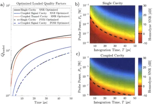
where -y = T/r for the loaded decay time 1/r = 2/-r, + 1/Ti, and k = T/ri. The result illustrates that the optimum loaded quality factor of the cavity is a function of both the integration time and intrinsic cavity quality factor. Optimizing the SNR with respect to
r and T2 yields the optimum loaded quality factor, Qloade = wo-r8/2, shown in Fig. 3-3(a)
(assuming an intrinsic quality factor
Qi
= , Veff = 10 3 (A/n)3, and A = 2.3 rIm), which produces the SNR shown in Fig. 3-3(b) for a 2.3 tm probe wavelength.a) 105 Optimized Loaded Quality Factors b) 10-i Single Cavity3
-- Single Cavity SNR Optimized --- Coupled Signal Cavity SNR Optimized
20
- Coupled Tunnel Cavity -SNR Optimized 2
- -- Single Cavity -FOM Optimized
- -Coupled Signal Cavity FOM Optimized a10-6
010 10- -10 10 20 30 40 50 S10- Integration Time, T [ps] 0, c) Coupled Cavity 0 le20 10-! 10 10 0 103 104 -10 10 20 30 40 50 LO 20 30 40 50
Time [ps] Integration Time, T [ps]
Figure 3-3: Ideal performance of the single cavity architecture. The signal-to-noise ratio (SNR, Eqn. 3.14)
and figure-of-merit (FOM, Eqn. 3.15) are optimized with respect to the coupling rates depicted in Fig. 3-1 (assuming an intrinsic cavity quality factor of 105, a 2.3 tm probe wavelength, and a cavity mode volume of Veff = 10- (A/n)3), yielding the optimal loaded cavity quality factors illustrated in (a). The resulting optimized SNR of a homodyne measurement on the displaced probe signal is shown in (b) and (c) for the single and coupled cavity configurations, respectively.
The results demonstrate that a SNR>1 is achievable within 50 ps for a sub- W probe power due to the all-optical gain afforded by the detection cavity. Notably, the optimal loaded quality factors (~104) for these short (sub-50 ps) integration times are much less than
Qj,
indicating thatQj
can be further reduced without substantial degradation of the detection SNR. Similar results are obtained for Vff = 101 (A/n)3 (corresponding to a readily fabricable cavity) as illustrated in Fig. 3-4; however, the input power required for high-SNRdetection within a given time increases.
The functional dependence of the FOM upon the coupling rates, on the other hand, is dominated by T2. The 72
1 term implies that T - -2, as T2 <
71, Ti. Optimizing the figure of merit with respect to T yields the optimization constraint
(8 + 4y)e-^ - 2(1 +y)e- 2 + 2y - 6 = 0, (3.17)
which is satisfied for -y =T/T 1.9. Introducing the coupling quality factor of each port,
Qn = wo/r, = worn/2, the equivalent condition for coupling
Q
isQFOM wT 3.8 (3.18)
Since 7, and therefore
Q,
is dominated by the fastest leakage path (i.e. the output coupler with decay time T2), the optimal solution for the figure of merit exists when Q2 " Qmax anda) Optimized Loaded Quality Factors b) 1
10
c) .1
/
S Single Cavity -SNR Optimized Coupled Signal Cavity -SNR Optimized -Coupled Tunmnel Cavity -SNR Optimized
igle a
- - - Single Cavity -FOM Optimized
- - Coupled Signal Cavity -FOM Optimized
50 100 150 200 250 Time [pa] 10 10 10 0 50 100 150 200 250 Integration Time, T [ps] 50 100 150 200 250 Integration Time, T [ps]
Figure 3-4: Optimized quality factors (a) and homodyne signal-to-noise ratios for the ideal single (b) and coupled (c) cavity detectors. For comparison to Fig. 3-3, each cavity is assumed to have a larger mode volume Veff = 10-'(A/n)3 at A = 2.3 km.
the input coupling is minimized (Qi -+ oc). The resulting peak FOM is
FOM ~ 0.381 Aw2T2 hw
0. (3.19) When comparing the detection performance and dark count rates, it is convenient to introduce a detection efficiency parameter T)SN = 1 - e , which quantifies the probability
of the integrated output signal crossing an optimum threshold level assuming shot noise limited detection [29]. The efficiency at optimal coupling is simply
r1SN = 1 - = 1 - eFOMa12 - 381Aw2 T2jaj2
/hW0 (3.20)
which demonstrates the dependence of the detection efficiency upon the intracavity probe
photon number Ja12/hwo.
3.2
Coupled Cavity Design
The coupled-cavity architecture shown in Fig. 3-1(b) can be used for "cavity dumping" to reduce the required probe power. As analyzed below, the waves s,+ =
j
2/'2e'dat andst+ =
j
2/7e3 as+j
2/T2eJ245at couple the tunnel and signal cavities, which are separatedby a distance corresponding to an effective phase
#.
If q = mir for any integer m, the wave output from a, destructively interferes with st+ at sout, corresponding to the high-Q regime of the two cavity system. The phase shift produced through the absorption of a signal photon within a, disturbs this interference condition, causing rapid evacuation of the stored cavity field. This effect, analogous to "cavity dumping" for pulse generation in laser resonators [30],io~ io~
I40-
30 20 10 0 -10I40
30 20 10 10 0 -10 105Probe Beam T T,
sout 72____2__ __ i
LOmlSfV 4
Homodyne Detector
Figure 3-5: Diagram of the coupled cavity photodetector, including signal amplitudes s and coupling rates 1/r. Depending on the spacing #, destructive interference between the signal cavity (a.) and tunnel cavity (at) decay paths can enable the signal cavity to be strongly coupled to the output waveguide while maintaining its intrinsic Q in steady state.
has been previously implemented to achieve ultrafast tuning of photonic crystal cavities [31]
and integrated ring resonators [32].
3.2.1
Architecture and Performance Metrics
These key improvements can be verified and quantified by analyzing the schematic shown in Figure 3-5. Here, a "tunnel" cavity is coupled to the output waveguide at a physical distance corresponding to an optical phase shift 4. Destructive interference between ss+, the light reflected from the signal cavity towards the output, and the leftward decaying light from the tunnel cavity results in energy storage within the system limited only by the input coupling and intrinsic decay rates. As a direct result of the amplified cavity energies, the required input power is reduced.
Assuming both cavities are tuned to the resonant frequency wo, the system shown in Figure 3-5 can be described by the coupled differential equations [26]
dat _ ( 1 ! 21 22 . = jwoat - - + - + -) at + j -sin + j -st+ (3.21) dt Ti 71 T2 T1 t2 1/-rt da8 (! a j1 =j a - - ++2j-ss+, (3.22) dt Ti T3 3 1/r8
where 1/T1, 1/72, and 1/T3 are the coupling rates at each port, 1/-ri is the intrinsic decay
rate of the cavities, 1/Ts (1/Tt) is the loaded decay rate of the signal (tunnel) cavity, s,+ =
3.2.2
Optimization
For maximum energy storage, we seek to satisfy
sot
(1 + ej
2") ass + j asei- 0.
(3.23)
Inserting the steady state conditions
-sin (SS)
(3.24) -t T2 T2 ( W-W) 1/-.) (.4
a ) T23 a (3.25)
and assuming resonant excitation, we find the condition
3 (1 +e- 22o) = 2. (3.26)
Ts
To enable rapid extraction of the probe field, the signal cavity is heavily coupled to the output waveguide such that T3
<
7i. In this case, T3 ~ T-, yielding the approximate solutionOoptimal = M7 (3.27)
for any integer m.
Given these considerations, we numerically optimized the coupling rates of Eqns. 3.24 and 3.25 to maximize the SNR in Eqn. 3.14, yielding the loaded quality factors shown in Fig. 3-3(a) and associated SNR in Fig. 3-3(c) and Fig. 3-4(c) [for the mode volumes Veff = 10-3 (A/n)3 and Veff = 10-1 (A/n)3, respectively]. These simulations indicate that the
power reduction is proportional to -Qi/Q3, which can be understood as the amplification of stored energy in the high-Q regime.
Note that, since the FOM is independent of input power, the coupled cavity architecture achieves the same optimum value of Eqn. 3.15 as that of the single cavity configuration.
3.3
Jitter
We also consider photodetector jitter, or timing uncertainty in signal photon detection, originating from three primary sources: 1) fluctuations in the signal photon absorption time, 2) probabilistic variation in the output probe field, and 3) the jitter of the classical homodyne detectors used to measure the phase shift of the transmitted probe field. For visible light, the first can be conservatively estimated by the absorption coefficient of room temperature, undoped silicon (aabs ~ 103 cm-1
[33]),
which corresponds to a 1/e absorption depth of 10tm and an associated absorption time on the order of 10 fs.
The second contribution, jitter introduced by statistical fluctuations in the probe field photon number, can be estimated using the results of the previous section. Assuming the
detector FOM is optimized, Eqn. 3.19 yields
Atth 1 Anp (tth) (3.28)
tth 2 (np(tth))
an estimate of the fractional uncertainty in a detection-threshold crossing time tth with
respect to the mean integrated output photon number (nr(tth)). Since the number of probe field photons output from the resonator within a differential time interval is governed by a Poisson distribution, np(tth) at tth is similarly Poissonian. For the large photon numbers
required for high-efficiency detection, the probability of m photons reaching the detector by
tth can be approximated by the Gaussian distribution
I(m) {m-(np(tth
912
P (m) e ' e 2(np(tth)) (129)
/27r(np(tth))
with a mean and variance equal to (np(tth)) [34]. If we define the jitter Atjitter to be time interval bounded by (np(tth)) nyl, where a-l, is the standard deviation of (np(tth)), Eqn. 3.28
simplifies to
Atjitter 1
(3.30)
tth VInp(tth)
Assuming (np(tth))
>>
1 as required for efficient photodetection, we see that the jitter from statistical variations of the output field is much smaller than tth --- on the order of 10 - 100ps for the fast operation regime of interest - and can in principle be sub-ps. Therefore, we find that the jitter from the first two sources is negligible in comparison to the jitter
associated with the classical probe field detectors.
3.4
Photon Number Resolution (PNR)
As an added benefit, the functional form of the SNR provided in Eqn. 3.14 shows that n, is proportional to the square of the resonance shift, and is thereby a function of the number of absorbed signal photons n,. Fig. 3-6 demonstrates this scaling for a 10 pW input probe power. For small n,, the trend is well fitted by considering the biexponential behavior of the refractive index shift in Eqn. 2.8. The growth of nr with respect to n. is large enough to enable photon number resolution of the signal field. This is illustrated by the well-separated Poissonian distributions of nr in the inset of Fig. 3-6 for n, E [1, 5].
3.5
Summary
Overall, these optimized results demonstrate that a single silicon nanocavity can enable ul-trafast, high-efficiency, and even number resolving single photon detection. Cavity dumping in a two-cavity system can reduce the probe field power by over an order of magnitude. This improvement also opens the possibility of monitoring a large array of detectors with a significantly reduced input probe power. Moreover, jitter contributions for the all-optical photodetector include fluctuations in the signal photon absorption time, probabalistic
vari-Photon Number Resolution
o
T=10ps Coupled Cavities 0 T=25pso
T=50ps -O , ... -x -0-x
-002-
' Sing- Cavty Ici.05 20 avt 102x - ~ ~ Single Cavity 1000 -'Kn0000.05
2 3 T =25 ps -0
OIAA
A.
0 np 500 100 1 1 1 2 3 4 5Absorbed Signal Photons, n,
Figure 3-6: Photon number resolution with cavity readout. Since the SNR is proportional to the square
of the frequency shift induced through free carrier dispersion, photon number resolution - as illustrated
by the plotted scaling characteristics for a 10 1 W probe power - is achievable. Black dashes show that
the trend is well fitted by considering the biexponential behavior of Eqn. 2.8. The inset depicts the well-separated Poissonian distributions of output probe photon number np generated from the absorption of n, signal photons.
ation in the output probe field, and the jitter of the homodyne photodetectors. As the first two are negligible for high-efficiency detection, the achievable jitter is limited by that of the photodetectors used to measure the classical probe field.
Chapter 4
Dark Count Rates and Mode Volumes
4.1
Dark Count Contributions
The aforementioned analysis considered the probe laser shot noise as the sole source of noise. In reality, dark counts - erroneous detection events which occur in absence of a signal beam
- must be carefully considered. Any fast (on the order of the detector integration time
T) change in the cavity refractive index greater than An contributes to the dark count
rate, as slow changes can be high-pass filtered. We consider three principal factors: thermal excitation of free carriers, temperature fluctuations of the semiconductor substrate, and multiphoton absorption. While surface defect states may contribute to the dark count rate, we omit this contribution due to the record-low surface recombination velocity of silicon
[35].
4.1.1
Thermal Noise
Thermally-Excited Free Carriers
The mean density of thermally-excited free carriers within a semiconductor at a given tem-perature - known as the intrinsic carrier concentration ni - is governed by the ratio of the material's bandgap to the environmental thermal energy and can be approximated with a Fermi-Dirac distribution. Due to the relatively large bandgap of silicon (Eg=1.1 eV), this relationship yields a negligible intra-cavity thermal carrier concentration for our proposed system. Specifically, for silicon at 300 K, the intrinsic carrier concentration is approximately
1.5 x 1010 cm , which leads to mean electron-hole pair population hcavity of -4 x 10⁻⁶ within the proposed cavity volume (Vff = 10 3
(A/nsi)
3)
at any given time. Since the mean free carrier lifetime (~ns [36]) is orders of magnitude longer than the detector integration times of interest (-10 - 100 ps), we assume a quasi-static carrier distribution during the detectorintegration time. In this case, the probability of a non-zero thermally-induced free carrier concentration can be estimated as
P{fncav > O} = I - Pfncay = 0} 1 -_cavity
)
cavity(4-cavity + 1
Kcavity
1 ncavity =0= 1 - 1 cavity. (4.2)
We therefore see that at 300 K the dark count probability is on the order of 4 x 10⁻⁶. Additionally, modest cooling dramatically reduces the thermal excitation probability. Since ni oc T3/2 Eg/2kTo,
where kB is the Boltzmann constant and To is the ambient tempera-ture, cooling silicon to 77 K decreases the intrinsic carrier concentration to on the order of
10-18 cm-3 . Given these metrics, we find that the density of thermally excited free-carriers
is negligible.
Temperature Drift
Temperature fluctuations, on the other hand, cannot be ignored if the temperature depen-dence of the cavity material's refractive index leads to index changes on the order of those produced by free carrier dispersion. The cavity therefore requires a temperature stability
ATo < Ansi/aTo (4.3)
which is dictated by the thermo-optic coefficient aTO of the cavity material. For our proposed cavity, silicon's thermo-optic coefficient of ~1.8 x 10⁻⁴ [37] thus demands sub-Kelvin (-0.1K)
temperature stability. The integration of a modern PID temperature controller, which can achieve sub-millikelvin temperature stabilization [38], will therefore minimize the rate of dark counts generated by temperature variations of the substrate.
Thermo-Refractive Noise
While slowly-varying (relative to the detection interval) temperature deviations can be high-pass filtered, fundamental statistical temperature fluctuations must still be considered. Within a semiconductor nanocavity of heat capacity Cv at temperature T, the magnitude of these fluctuations can be estimated as [39, 40]
(6T) kBT2 (4.4)
PC/VT,
where kB is the Boltzmann constant and the result assumes complete confinement within the dielectric medium.
As shown in [39], the proper form of VT can be found by solving the heat equation
dtk6T (tr) - DTV26T(t, i) = FT(t, r) (4.5) in frequency space: d d T(t, i?) - DTV26T(t, ?) = FT(t, r) dt jw6T(w, k) + DTIk126T(w, k) = F(w, k) _# F(w , ) 6T(w, k) = ,(46) jw + DTIkI 2
Taking the temperature mode average
- - 1
6T(t) = 1 Veff and inverse Fourier transforming yields
6T(t) = (27) 4Vf d ;) 2
(27)4Va J max{|E() 2} We can then solve for the autocorrelation of 6T:
T)) = (max |21 - 2 d3 6(fi)E(i12 j d 3 -2 ejk2.2 (F(wi, ki)F*(w2, k2)) (jWi + DTrki l2)(-jw 2 + DTIk212) (4.9) Using the frequency-space autocorrelation of the Langevin driving force [41],
(F(wi, k1)F*(w2, k2)) = (27 )42kBO2DT k 26( - k2)6(wI
PCv we can simplify to (6T(t)6T*(t + T)) = (MaX{fE(i)1 2})-2
2kBT02DT
(27r)pcvI
dw e-jw-d3i2 E(f2)| ()j 2ek(ri2) 1 w2 + D k14 _ maxfe (j;*)12})-2 2kBT02DT (27r)pcv x dw P W 2+ Dj~kJ4 -j-r (max{EE(r 12})- 2 2kBT02DT (27r)4VKef PCVI
I
d3 Ik 2 d I 2 2~f ~2jk.if 2 DTI k12 Z (max{E(i) 2}- 2 kBT02DT dk EDT|k|2Tf
) 2 2 (4.11) Eqn. 4.11 must equal Eqn. 4.4 for -r = 0, which reveals the final solution for the thermalf 6T (, t) F(f) 2 maxfEIE(F)121 (4.7)
I
dw ejWt (6T(t)6T*(t +Idak
ej .F F(w, k) f jw + DTrk12 (4.8) Id3-2 xJ xJ dw, ewtf
dw2 ejw2(t+T) dak1 ejkl (4.10)I
d3k 2k(6T(t) 6T*(t
+ T)) = e(Y2)|Z(,)12 - W2), x 3- C( I- - 2/d rrE
,
mode volume VT: (6T2) = (max{4| ()j2}>2 kBT2DTf dk f37-.--.2 f 2 _k (2w)3V 27)3V PCv dPk dVVT 3 1 e kBT (4.12) =~ VT = (2-r)3Vef(max{cEJ(j?) 2})2
f
dak f d3()()2ei~ 2 V 2 ax j|$())22e2 f dBr* E( r21 () 14 f daa, Etr)2 If r14 Max{<2|fl4l 2 eff where (2) f d 3 r* (T121 E 14 Ve)
=2I4 (4.14) max{e2 E 4}is equal to the two photon absorption mode volume introduced in Sec. 4.2 (assuming complete confinement of the mode within the semiconductor). This result matches Gorodetsky's original result [39] with the exception of different normalization conditions.
Given T = 300 K, p = 2.3 g/cm3, Cv = 0.7 J/g-K, Vff = 10-3(A/ns) 3, and
V
2 ~(A/ns andeff
0.075Veff (as estimated from the ultrasmall mode volume "tip" cavity profile in Fig. 4-5), Fig. 4-1 shows that the resulting temperature fluctuations - which typically limit PhC cavity sensitivity [40] - yield index changes that are an order of magnitude weaker than those produced from the absorption of a single photon. Therefore, we omit thermo-refractive noise from our analysis. Note that the reduced thermal mode volume VT < Vff characteristic of the ultrasmall mode volume tip cavity is key to this conclusion - if VT ~ Veff, the standard deviation of the thermo-refractive noise is on the same order of magnitude as the single photon-induced index change. Chapter 4 contains a detailed analysis of this mode volume-based noise suppression.
4.1.2
Multiphoton Absorption
While both thermally induced free carriers and direct index variations due to the thermo-optic effect in silicon can be mitigated with proper environmental control, multiphoton ab-sorption (MPA) events - given the indistinguishably between probe- and signal-induced free carriers within the cavity - produce a dark count rate that can only be lowered by mini-mizing the intensity of the probe laser within the signal cavity, and thus inherently reducing the sensitivity of the detector. The dark count rate from a kth order nonlinear absorption
(kPA) rate dnkMPA (under the assumption that each multiphoton absorption event contributes
a dark count) is [42]
Rdark - dK'A _ /3 1kaVkPA, (4.15)
Comparison of FCD and Thermo-refractive Noise (TRN) Index Change 0 -T =200 K -- T =250Koo 50- -- T= 300K- 40- 30- 20-10 ' 1.5 2 2.5 3 3.5 4 4.5
Probe Wavelength A [,am]
Figure 4-1: Comparison of relative magnitude of single photon-induced free carrier dispersion and thermo-refractive noise index changes for various probe wavelengths and temperatures assuming the parameters stated in the text.
where VkPA is the mode volume for k-photon absorption processes (derived in the subsequent
section)
VkPA = fsemi semi IE(I d r (4.16)
Max E~k ij |2kjsem
3
k is the corresponding multiphoton absorption coefficient, and Imax = ja12c/2nsiVeff is the peak intracavity intensity for a silicon cavity with index nsi, optical mode volume Veff, and
stored energy ja12. The dark count rate can thus be approximated as
Rdark = 3k c * VkPA 2(4.17)
khwo 2nsi ) V e
In standard photonic crystal cavities, the intensity variation within the optical mode volume is relatively small, such that the multiphoton absorption mode volume can be ap-proximated as equal to that of the optical mode (for example, V2PA = 2V'2Veff assuming a Gaussian intensity distribution in a uniform medium). However, the ultrasmall mode volume
(Vff < (A/n)3) photonic crystal cavities of interest for this work [11, 12, 14] contain local-ized defects which amplify the optical intensity within small regions of the diffraction-limited mode size, Vmin ~ (A/2n)3 [43]. In this case, as further explored in the following section, VkPA - and therefore the dark count rate for a given detection efficiency - can be several orders of magnitude lower than the value provided by this estimate.
4.2
Dark Count Mode Volumes
4.2.1
Derivation
Since the multiphoton absorption (MPA) rate is proportional to Ik for k > 2, we are
absorption event order. The dark count rate density - the number of multiphoton absorption events per unit volume per unit time - for kth order absorption events at a position r' is defined as [42]
rdark ) = I). kN (4.18)
khwo
For a non-uniform intensity profile, the total dark count rate can be directly evaluated by integrating the dark count rate density over the semiconductor, where MPA can occur:
Rdark = rdark(ri d r
J
klI(r)d r. (4.19)Alternatively, the integration can be replaced through the introduction of an "effective MPA mode volume" VkPA, which leads to the simple relation
A /k
Rdark = Ikw iaxVkPA (4.20)
khw0
where Imax = Ia|2c/2nVff is the peak intensity resulting from the confinement of a total cavity energy ja12 within the standard optical mode volume Veff. Here, we seek to define
VkPA. Given I(f) = (c/2n)EoIEI2, Equation 4.19 simplifies to
Rdark = khw0
J.mi
2n(id )k. (4.21)k;0 esei n
Assuming a homogeneous semiconductor medium of index nsemi, we find
Rdark = ktiwo ke
I
E 2kd r, 2?2semi (4.22) / semiwhich can be re-expressed as follows to realize the standard mode volume form: Rdark~ ~ k1W (2f2 mx{sm })fsemi EemiIE(712kd3i?
Rdark = ko 2n max mx semi skmil *I2d . (4.23)
keerhdsemi od|lu2 ,srdxPesAe
VkPA
Therefore, the desired MPA mode volume is
- fsemi semi I kd3 . fsemi I
)
2kdV IVkPA = ( sa
{emi.|$2 max{ E2k}
(4.24)
Intuitively, VkPA is analogous to the standard Veff with two differences: 1) it is evaluated as a weighted average of volume with respect to higher orders of the field energy density as desired for MPA processes (oC Ik), and 2) it is only evaluated over the dielectric region of the PhC, where MPA can occur.