Development of Optical Field Emitter Arrays
byYujia Yang
B.S. Electronics Science & Technology Zhejiang University, 2011
SUBMITTED TO THE DEPARTMENT OF ELECTRICAL ENGINEERING AND COMPUTER SCIENCE IN PARTIAL FULFILLMENT OF THE
REQUIREMENTS FOR THE DEGREE OF
MASTER OF SCIENCE IN ELECTRICAL ENGINEERING AND COMPUTER SCIENCE
AT THE
MASSACHUSETTS INSTITUTE OF TECHNOLOGY SEPTEMBER 2013
C Massachusetts Institute of Technology 2013. All rights reserved.
Signature of Author:
Department of Electrical Engineering and Computer Science August 30, 2013
Certified by:
Professor of Electrical
Karl K. Berggren Engine mg and Computer Science Thesis Supervisor
Accepted by:
Leslie A. Kolodziejski Professor of Electrical Engineering and Computer Science Chairman of the Committee on Graduate Students
Development of Optical Field Emitter Arrays
byYujia Yang
Submitted to the Department of Electrical Engineering and Computer Science on August 30, 2013 in Partial Fulfillment of the Requirements for the Degree of
Master of Science in Electrical Engineering and Computer Science
ABSTRACT
Optical field emitters are electron emission sources actuated by incident light. Optically actuated field emitters may produce ultrafast pulses of electrons when excited by ultrafast optical pulses, thus making them of interest for specific applications such as ultrafast electron microscopy, diffraction and spectroscopy; and as electron sources for X-ray generation. Recently proposed intense, coherent, and compact X-ray sources require low emittance, high brightness and short duration electron bunches that form a periodic pattern in the transverse plane. This thesis theoretically developed optical field emitter arrays that are suitable for use as the electron source for this novel X-ray source. Studies of several optical field emitter array structures, including vertically-standing gold nanopillars and silicon tips, in-plane gold nanostructures, and metallic line gratings, were performed via theoretical analysis and numerical simulations. Enhancement of the optical near-field and power absorption was achieved by geometrical and plasmonic effects, leading to enhanced charge yield from the optical field emitter arrays.
Thesis Supervisor: Karl K. Berggren
Acknowledgements
First of all, I would like to express the deepest appreciation to my research supervisor, Prof. Karl Berggren, for his invaluable assistance, guidance and suggestions during the past two years of my graduate study. Without Karl, I would never have the chance to enter the wonderful nano-world and immerse myself in the beauty of nanoscience and nanotechnology, and the work in this thesis would have been impossible. And congratulations to Karl on his recent appointment as a full professor!
I would also like to express my sincere thanks to Dr. Richard Hobbs for his effort in developing the fabrication process and preparing most of the samples, his valuable discussions on my research work, his important suggestions on revising this thesis, and his patient guidance to improve my cleanroom experience and lab skills.
In addition to Karl and Richard, I would like to thank all the people on the project
Compact and Ultrafast Bright and Intense X-ray sources (CUBIX), including but
not limited to, Prof. Franz Kaertner, Dr. William Graves, Dr. Luis Velasquez-Garcia, Dr. Michael Swanwick, Dr. Arya Fallahi, Donnie Keathley and Eva De Leo. Their discussions and suggestions greatly improved my work.
Besides, I am grateful to Jim Daley, Mark Mondol and other NanoStructure Laboratory (NSL) staff for running a great lab where the samples were fabricated, and to Tim McClure for training me on UV-Vis measurement that optically characterized the samples.
Additionally, I would like to express my gratitude to Prof. James Fujimoto, my academic advisor and the lecturer of the course 6.631 Optics and Photonics, for making me clear about and reminding me of the timeline of graduate study in EECS, MIT and giving me excellent lectures on optics, and to Prof. Terry Orlando for kindly guiding me through the process of finding a research home and releasing my confusion when I first started my graduate study two years ago.
Moreover, I want to thank all my colleagues, labmates, classmates and friends for bringing inspirations, knowledge and happiness to my graduate school experience. In terms of funding, I would like to appreciate Jin Au Kong Memorial Fellowship
for supporting my graduate study in Fall 2011 and DARPA for supporting the CUBIX project.
Finally, I am truly indebted to my Mom and Dad living thousands of miles away in China. Despite the distance between us, their love and support are always around me and beyond words can describe.
Contents
Chapter 1: Ito
uto ...
1
1.1 Electron Field Emission and Field Emitter Arrays (FEAs)...15
1.2 Photo-induced Electron Emission and Optical Field Emitters ... 16
1.3 Metallic Photocathodes and Surface Plasmon Resonance...17
1.4 Previous Work on Optical Field Emitters ... 19
1.5 Summary of Work ... 21
Chapter 2: Theory of Electron Emission and Surface
Plasmon Resonance... 23
2.1 Electron Emission Theory ... 23
2.1.1 Therm ionic Em ission ... 23
2.1.2 Static Field Em ission ... 25
2.1.3 Photoelectron Em ission... 28
2.2 Electromagnetics Theory...31
2.2.1 M axw ell's Equations... 31
2.2.2 W ave E quation ... 32
2.2.3 B oundary Conditions ... 32
2.2.4 Constitutive Relations and Material Properties ... 33
2.2.5 Quasi-Static Approximation ... 34
2.2.6 N ano O ptics... 35
2.3 Surface Plasmon Resonance...36
2.3.1 Electromagnetic Properties of Metals... 36
2.3.2 Surface Plasmon Polariton (SPP)... 38
2.3.3 Localized Surface Plasmon Resonance (LSPR)... 42
2.4.1 Absorption Cross Section and Temperature Rise ... 46
2.4.2 Femtosecond Laser Photothermal Damage of Plasmonic Nanoparticles 47 2.4.3 Electron Tem perature... 49
2.5 N um erical Sim ulations ... 50
Chapter 3: Modeling of Vertically-Standing Gold
Nanopillars
and Si Tips...****
....
**.*...53
3.1 Infinite Length Conical Gold Tip in Water...53
3.1.1 Two-Dim ensional (2D) M odel... 53
3.1.2 Three-Dimensional (3D) M odel... 55
3.2 Gold Islands and Gold Pillars... ... ... 57
3.2.1 Gold Islands ... 57
3.2.2 G old Pillars... 58
3.3 Plasmonics Enhanced Gold Nanopillar... . ...59
3.3.1 Gold Nanopillar in Vacuum ... 59
3.3.2 Gold Nanopillar on Silicon Substrate with Titanium Adhesion Layer.... 60
3.3.3 Tungsten Nanopillar on Silicon Substrate ... o ... 62
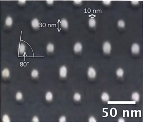
3.4 Fabricated Gold Optical Field Emitters... ... 63
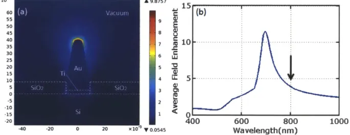
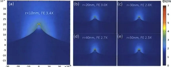
3.4.1 Near-field Profile and Field Enhancement Spectrum...64
3.4.2 Geometry Optimization of the Fabricated Au Optical Field Emitter ... 66
3.5 Field Enhancement by Silicon Tips... 72
3.5.1 Sharp Si T ip... 72
3.5.2 B lunt Si M esa... 74
3.6 Electrostatic Field Enhancement .... ... ... 77
3.7 Electromagnetic Heating of Optical Field Emitters...79
3.7.2 Polarization Dependence of Electromagnetic Heating of Au Nanopillars ... 8 2
3.7.3 Heat Radiation from Au Nanopillars ... 83
3.7.4 Electromagnetic Heating of Fabricated Au Optical Field Emitter ... 85
3.7.5 H eating of Si Tips ... 91
Chapter 4: Modeling of In-Plane Gold Nanostructures... 93
4.1 Single Gold Nanorod...93
4.1.1 Single Gold Nanorod in Vacuum... 94
4.1.2 Single Gold Nanorod on Dielectric Substrate... 95
4.2 Substrate Effect on Gold Nanorod Plasmon Resonance...97
4.3 Gold Nanorod Array on Silicon Substrate ... 100
4.3.1 G eom etry O ptim ization... 101
4.3.2 O ptical N ear-field Profile... 102
4.4 Fabricated Gold Nanorod Optical Field Emitter Arrays...103
4.4.1 Fabricated Gold Nanorod Array on Si Substrate ... 105
4.4.2 Fabricated Gold Nanorod Array on ITO Substrate... 108
Chapter
5:
Modeling Metallic Line Gratings... 111
5.1 Copper Grating on Silicon Substrate...112
5.1.1 M odel S etup ... 113
5.1.2 Line Width Optimization: Surface Plasmon Polariton Cavity ... 114
5.1.3 Line Thickness (Height) Discussion: Validity of Constant Quantum-E fficiency A ssum ption ... 120
5.1.4 Grating Pitch Optimization: Rayleigh Anomalies ... 120
5.1.5 Metamaterial Behavior of Copper Gratings... 127
Chapter 6: Summary and Future W ork... 129
List of Figures
Fig. 1.1. Layout of the emittance exchange ICS X-ray source...17 Fig. 2.1. Schematic for thermionic emission from metal to vacuum...24 Fig. 2.2. Schematic for static field emission from metal to vacuum...26 Fig. 2.3. Schematic for optical field emission and multiphoton emission from a m etal to vacuum ... 29 Fig. 2.4. Surface plasmon polariton wave confined at a metal/dielectric interface.40 Fig. 3.1. Simulation of optical field enhancement by a 2D subwavelength conical A u tip in w ater... . . 55 Fig. 3.2. Simulation of optical field enhancement by a 3D subwavelength conical A u tip in w ater... . . 56 Fig. 3.3. Gold island optical-field emitter...58 Fig. 3.4. Gold pillar optical-field emitter... 59 Fig. 3.5. Simulated near-field enhancement profile for Au nanopillars in v acu u m ... 6 0 Fig. 3.6. Simulated near-field enhancement profile for Au nanopillars on Si substrate with Ti adhesion layer... 62 Fig. 3.7. Simulated near-field profile for W nanopillars on Si substrate... 63 Fig. 3.8. SEM image of fabricated Au nanopillars...64 Fig. 3.9. Simulated optical field enhancement of the fabricated Au optical field
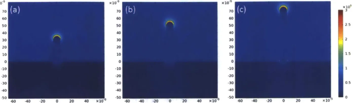
em itter...6 5 Fig. 3.10. Simulated optical near-field of fabricated Au optical field emitters with various em itter heights... 67
Fig. 3.11. Simulated optical near-field of fabricated Au optical field emitters with various em itter base radii... 68
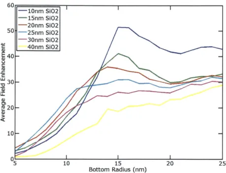
Fig. 3.12. Simulated average field enhancement for fabricated Au optical field emitters with a fixed shape and varying size...69
Figs. 3.13-3.15. Numerically calculated average field enhancement factor of fabricated Au optical field emitters with varying sidewall angle and base radius..71
Fig. 3.16. Optical field enhancement by Si tips... 74
Fig. 3.17. Blunt Si mesa structure...75
Fig. 3.18. Simulated optical near-field enhancement profile of the blunt Si mesa stru ctu re...7 7
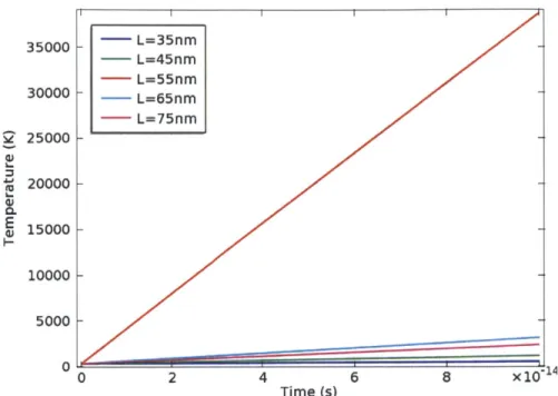
Fig. 3.19. Simulations of electrostatic field strength...79 Fig. 3.20. Simulated average temperatures of Au nanopillars with different lengths in v acu u m ... 8 1
Fig. 3.21. Simulated temperature profiles of Au nanopillars in vacuum...81
Fig. 3.22. Simulated average temperatures of Au nanopillars with different polarizations of incident light...83
Fig. 3.23. Simulated Au nanopillar average surface temperature as a function of electromagnetic heating time...84
Fig. 3.24. Simulation of electromagnetic heating of fabricated Au optical field em itter...8 7
Fig. 3.25. Simulation of the average temperature of the emitter as a function of time with varying surface emissivity values... 88 Fig. 3.26. Estimated temperature rise at a certain distance away from the emitter.89
Fig. 3.27. Temperature and optical field enhancement profiles of the fabricated Au optical field em itter... 90
Fig. 3.28. Simulated temperature profile of the Si tip heated by incident plane w av e ... 9 2
Fig. 4.1. Model setup and FEM meshing for simulating a single Au nanorod in vacuum or on a substrate... 94 Fig. 4.2. Simulated normalized optical power absorption spectra and field enhancement spectra for a single Au nanorod in vacuum...95 Fig. 4.3. Simulated normalized optical power absorption spectra and field enhancement spectra for a single Au nanorod on two different substrates...96 Fig. 4.4. Optical near-field enhancement profile for Au nanorods on two different su b strates...9 7 Fig. 4.5. Simulated normalized optical power absorption spectra for a single Au nanorod on different substrates with various gap distances...99 Fig. 4.6. Optical near-field profile for Au nanorods with various gap distances to th e su b strate...100
Fig. 4.7. Model setup and FEM meshing for simulating Au nanorod arrays on Si su b strate ... 10 1 Fig. 4.8. Simulated normalized optical power absorption spectra and average field enhancement spectra for Au nanorod arrays on Si substrate with various aspect-ratio s...10 2 Fig. 4.9. Optical near-field enhancement profile for the optimal Au nanorod on Si su b strate ... 10 3 Fig. 4.10. Model schematic of fabricated Au nanorod optical field emitter array s...10 4 Fig. 4.11. SEM image of fabricated in-plane Au nanorods...104 Figs. 4.12-4.13. Simulated normalized optical power absorption spectra and average field enhancement spectra for fabricated Au nanorod array on Si with the Ti adhesion layer and Si0 2 thin film ... 106 Fig. 4.14. Simulated normalized optical power absorption spectra and average field enhancement spectra for fabricated Au nanorod arrays with and without Ti adh esion lay er...108
Fig. 4.15. Simulated normalized optical power absorption spectra, average field enhancement spectra, and optical near-field profiles for Au nanorod arrays on a Si or IT O sub strate...110
Fig. 5.1. Model setup and coordinate definition for modeling metallic line grating optical field em itter arrays...114
Fig. 5.2. Simulated power absorption of an individual Cu line under TM and TE illuminations as a function of Cu line width and thickness...115
Fig. 5.3. Simulated width-dependent power absorption for TM illumination...116 Fig. 5.4. Magnetic field profile (Hz) for SPP cavity modes...117
Fig. 5.5. Simulated Cu line width dependent power absorption for different optical w av elen gth s...1 19
Fig. 5.6. Simulated power absorption of a Cu line grating under TM and TE illuminations as a function of line width and grating pitch...121
Fig. 5.7. Simulated pitch-dependent power absorption for both TE and TM illu m in ation s...12 2
Fig. 5.8. Schematics showing Rayleigh's explanation for Wood's anomalies...123 Fig. 5.9. Simulated Cu grating pitch dependent power absorption for different
optical w avelengths...124
Fig. 5.10. Simulated absorption spectra of Cu grating with various pitches under TE or TM illum ination...125
Figs. 5.11-5.12. Simulated absorption spectra of Cu grating with various pitches under TE or TM illumination, without spurious modes...126 Fig. 5.13. Metamaterial behavior of Cu grating under TE illumination ... 128
Chapter 1: Introduction
1.1 Electron Field Emission and Field Emitter Arrays (FEAs)
Electron field emission (also known as field emission, field electron emission and field-induced electron emission) refers to the phenomenon that materials emit electrons under a strong electric field. The devices that field-emit electrons are called field emitters. Generally speaking, the field emission materials can be of solid, liquid as well as molecular and atomic forms, but here we primarily focus on electron emission from solids, especially metals and semiconductors since sufficient supply of electrons is needed.
Electrons are held in solids or molecules by Coulombic forces due to the positive charge on the nuclei of atoms within. Extraction of electrons from a solid thus requires energy which has to be supplied to the electrons to overcome the material work function and escape to vacuum. The energy source can be heat or incident photons, with the corresponding electron emission phenomena termed thermionic emission and photoelectric effect, respectively. However, electrons can also escape a work function barrier via quantum tunneling, where no extra energy is required. The basic idea of field emission is to induce a strong electric field at the material surface, which reduces the thickness of a work function barrier and facilitates electron tunneling. As the energy of tunneling electrons is around the Fermi level (for metals) or the conduction band edge (for semiconductors) that is well below the vacuum energy level, field emission is also called cold field emission.
Field emission has a long history, dating back even before J. J. Thomson's identification of the electron [1]. The well-known electrical discharge around a
sharp point, the so-called "lightning rod effect", is an example of field emission, where the small radius geometry of an electrically conducting material causes electric field line crowding and enhances the field strength at the tip, inducing electron emission. The first quantum mechanical explanation of field emission was proposed by R. H. Fowler and L. W. Nordheim [2], after whom the "Fowler-Nordheim equations" are named. Although this theoretical treatment was derived for bulk metals, it remains as a reasonably good approximation for various materials and emitter architectures.
Electron field emission has a wide range of applications. One example is the vacuum tubes, the building blocks of first generation electric computers. Another example is electron-gun sources. Modem high resolution micro-/nano- metrology and fabrication tools, such as scanning electron microscopy (SEM), transmission electron microscopy (TEM) and electron beam lithography (EBL), all benefit from a high brightness electron source, where field emission is advantageous over thermionic and Schottky emission (combination of thermal and field induced emission). Electron field emission sources are also widely used in particle accelerators.
A field emitter array (FEA) is an array of a large number of individual field emitters. It is a large-area field emission source capable of generating a field emission current thousands and even millions of times larger than that from an individual field emitter. The first form of FEAs was the Spindt array, named after the inventor, C. A. Spindt, consisting of an array of sharp, conical-shaped
molybdenum tips embedded inside holes of an oxide film, on which an extraction gate was deposited [3]. The FEA is compatible with standard silicon-integrated-circuit fabrication techniques and has potential applications in field emission displays and multi-beam electron-beam lithography.
1.2 Photo-induced Electron Emission and Optical Field Emitters
Electron field emission can be achieved by applying a static electric field as well as optical illumination. Optical field emitters, also named as photocathodes, are electron emission sources excited by incident light.
A monochromatic continuous electromagnetic wave can be treated as a time-harmonically oscillating electric field at the emission site, and thus it is capable of inducing electron emission as long as the electric field amplitude is sufficient. The underlying physical mechanism is complicated by the photoelectric effect, where electrons are excited through the absorbing of photons. It is important to differentiate optical field emission, where the strong electric field associated with the electromagnetic wave induces electron emission, from single/multi-photon emission, where the energy of a single, or multiple, photons is absorbed by an
Optical field emitters are superior to conventional static field emitters as ultrafast electron sources, from which the electron bunches have a temporal duration of picosecond and even femtosecond time scale. For static field emitters, the switching speed of control electronics is too low to achieve ultrafast electron emission, whereas optical field emitters can be triggered by a picosecond or femtosecond laser to generate electron bunches with very short time span, which is favored by specific applications such as ultrafast electron diffraction [4][5] and ultrafast electron microscopy [5][6].
Optical field emitter arrays can be used as the electron sources for X-ray generation. Short wavelength radiations such as X-rays can be produced by illuminating relativistic electrons with longer wavelength lasers. The energy is transferred from high energy, relativistic electrons to low energy, long wavelength photons and hence high energy, short wavelength photons are generated, a mechanism called inverse Compton scattering (ICS). Very recently, Graves et al. proposed an idea of intense, coherent and compact X-ray sources [7]. It starts with periodically bunched electrons accelerated to relativistic speed, and the transverse periodicity is then converted to longitudinal density modulation via emittance exchange, from which X-rays can be generated by ICS (Fig. 1.1). This emittance exchange ICS X-ray source requires low emittance, high brightness and short duration electron bunches that form a periodic pattern in the transverse plane. Therefore, nanoengineered and femtosecond laser actuated optical field emitter array is an ideal option as the electron source for this application.
JN T- Dipoles
IR laser
Gun Nanocathode RF cavity Quadrupoles
IradiantlCS
RF deflecting cavity
Fig. 1.1. Layout of the emittance exchange ICS X-ray source [7]. Key components are (from left to right): nano-photocathode, RF acceleration cavity, quadrupoles for emittance exchange, And inverse Compton scattering (ICS).
1.3 Metallic Photocathodes and Surface Plasmon Resonance
Photocathodes can be made of either metals or semiconductors. Semiconductor photocathodes usually have high quantum efficiency, but suffer from current saturation due to electron depletion and finite response time due to electron
velocity saturation and transit time in the depletion region. The response time can be worsened by inclusion of electron diffusion time if both depletion region and neutral region are illuminated. Moreover, since surface states and contaminations can dramatically change the electronic and optoelectronic properties of semiconductors, ultra high vacuum is required for semiconductor photocathodes. Metallic photocathodes, on the other hand, have short response times and reduced vacuum requirements due to their robustness. But their efficiency is usually low. For instance, the quantum efficiency of copper, a commonly used material for metallic photocathodes, is on the order of 10-.
One way to enhance the efficiency of metallic photocathodes is to excite surface plasmon resonances. The strong electric field required in electron emission is usually achieved via the lightning rod effect, where a sharp structure crowds the equipotential lines. Since the electric field strength is proportional to the equipotential line density, the field is enhanced around the structure. As for photoelectron emission from metals, an additional mechanism, surface plasmon resonance, helps to assist field enhancement and electron emission.
Surface plasmon resonance refers to the collective oscillation of electrons in a solid coupled with oscillating electromagnetic fields and is confined at the surface of the solid. A strongly enhanced electric near-field is always associated with the surface plasmon resonance. Both the field enhancement and field localization are favored by optical field emitter arrays, since the charge yield of the emitters can be greatly improved. The materials generally used in surface plasmon resonance applications at optical frequencies are metals with high electrical conductivity such as Au, Ag, Cu, and Al, due to their negative dielectric permittivities in the visible frequency range and the fact that damping of surface plasmon resonance in these metals is minimal so that the resonance has a long life time (up to tens of femtoseconds) and a long propagation distance (up to tens of micrometers). Among them, noble metals like Au and Ag are ideal choices because their resistance to oxidation and corrosion can improve the robustness and lifetime of the optical field emitter arrays.
There are two key elements in the area of surface plasmon resonance, surface plasmon polariton (SPP) and localized surface plasmon resonance (LSPR). The former refers to the propagating surface plasmon wave confined at a metal/dielectric interface, while the latter the plasmon resonance localized at the
surface of a nanoscale metallic particle. Both SPP and LSPR can be utilized to enhance the electric field of optical field emitters.
1.4 Previous Work on Optical Field Emitters
Photoelectron emission from a single metallic optical field emitter, especially the emission of femtosecond-scale electron pulses, has been intensively studied recently to reveal the underlying physics of electron emission triggered by the interaction between ultrafast laser pulses and electron emitters. Hommelhoff et al. first studied this phenomenon by illuminating a tungsten tip with 810 nm Ti:sapphire laser [8]. Dependence of electron emission on laser power, polarization and DC voltage was investigated. They showed two emission processes: single-photon assisted DC field tunneling and strong optical field tunneling. They also demonstrated sub-cycle photo-electron emission in the strong optical field tunneling regime and theoretically showed sub-femtosecond electron pulses can be produced [9]. Ropers et al. studied multiphoton electron emission using low power femtosecond Ti:sapphire laser pulses to illuminate metal tips [10]. They primarily focused on the effects of DC bias voltage and incident laser power on electron emission and observed different power dependences under different DC bias voltages. In their theoretical model, the incident laser gave rise to a non-equilibrium electron distribution and electron tunneling through the work function barrier was caused by the DC bias voltage. Barwick et al. studied the electron emission mechanism by measuring the electron counts from a sharp tungsten tip illuminated by a near-infrared laser [11]. Electron emission was shown to depend on laser power, polarization and applied DC voltage. Yanagisawa et al. showed photoelectron emission from a single crystal tungsten tip and the selectivity of the emission sites [12]. The emission from different crystal surfaces was controlled by the polarization and incident angles of the laser pulses. Bormann et al. studied photoelectron emission from a gold tip operating in optical field emission regime [13]. The transition from multiphoton emission to optical field emission was observed by increasing the laser pulse energy. Schenk et al. demonstrated above-threshold photoemission with a photon order up to 9 from a sharp single crystal tungsten tip [14]. Peak suppression and threshold shifting observed from the electron energy spectra were indicative of the onset of strong field effects. KrUger et al. investigated attosecond electron emission from a tungsten tip and showed
carrier-envelope-phase (CEP) modulation of the energy spectra of emitted electrons [15]. The spectra were shown to be affected by the interference of sub-cycle emitted electron wave packets and electron re-scattering from the tip surface.
In addition to single-tip optical field emitter, optical field emitter arrays based on various materials and device architectures have also been reported, starting from the study of semiconductor optical field emitter arrays dating back to 1970s. Photo-assisted field emission from Si tip arrays was investigated by Thomas and Nathanson [16], Schroder et al. [17], Aboubacar et al. [18][19], Liu et al. [20], and Chiang et al. [21]. Hudanski et al. designed a carbon nanotube (CNT) based photocathodes by attaching CNTs to silicon p-i-n photodiodes [22]. In their design, photon-electron conversion and electron emission were separately performed by photodiodes and CNTs, respectively. In these studies on semiconductor optical field emitter arrays, the electron emission was induced by the applied electrostatic field and the photo-modulation was achieved by generating electron-hole pairs, and thus increasing the supply of electrons, which is very different from recently proposed multiphoton emission and optical field emission mechanisms. Zeier et al. reported optically enhanced electron emission from gold nano-pin-forest cathode [23]. The laser energy was coupled into and heated the pins, inducing thermionic or thermo-field emission. Mustonen et al. recently developed gated molybdenum (Mo) optical field emitter arrays fabricated by molding [24]. The electrostatic field together with a femtosecond laser pulse induces the emission of 5 pC electron bunch from the array.
Surface plasmon enhanced electron emission also gained researchers' attention recently as surface plasmon resonance can offer a high field enhancement factor and thus high electron emission yield. Irvine et al. showed electron emission and acceleration by surface plasmon polaritons on a thin film silver surface [25]. Electrons were generated via three-photon-assisted multiphoton emission and
accelerated by surface plasmons, gaining kinetic energies up to 0.4 keV. Iwami et al. reported plasmon-assisted field emission from fused silica tip arrays coated with gold thin film [26]. Linear fitting of data in a Fowler-Nordheim plot indicated the emission mechanism was field emission. Nagel et al. studied photo-induced electron emission from lithographically defined, electrochemical deposited gold nanopillar arrays [27]. The effect of surface plasmons on electron emission and acceleration were revealed from the energy spectra of emitted electrons. Li et al.
patterned copper photocathode surface with nano-hole arrays [28]. The excitation of surface plasmon polaritons on the periodically structured metal surface enhanced optical power absorption and hence photoelectron emission yield. Polyakov et al. fabricated a metallic grating structure as the photocathode, of which the optical power absorption was enhanced by metamaterial plasmonic resonance [29]. Thus, the photoelectron emission was greatly enhanced and showed dependence on the polarization of incident light.
1.5 Summary of Work
The goal of this thesis is to develop optical field emitter arrays that meet required specifications, which cannot be satisfied simultaneously by previously proposed design, as the electron source for emittance-exchange ICS X-ray sources. Specifically, the primary focus is on ultrafast response, low emittance, and enough charge yield of the optical field emitter arrays. Femtosecond and even sub-femtosecond ultrafast response can be achieved via actuation of metallic emitters with femtosecond laser pulses. Low emittance will be achieved by using small emitters with tens of nanometers scale and thus reducing the emission area. Requirements on charge yield can be met by making high density arrays and utilizing surface plasmon resonance enhancement.
Chapter 2: Theory of Electron Emission and Surface
Plasmon Resonance
2.1 Electron Emission Theory
Depending on the driving mechanisms, there are several different mechanisms of electron emission: thermionic emission, static field emission and photo-electron emission.
2.1.1 Thermionic Emission
Thermionic emission is electron emission induced by heating the emitting material, where electrons gain enough thermal energy to overcome the vacuum potential barrier and escape the material surface. For simplicity, we take metals as example emission materials. Electrons confined in a metal can be treated as a free electron gas and have an energy distribution described by the Fermi-Dirac distribution:
1
f(E) = 1 (2.1)
e(E-EF)IkBT +
Here EF is the Fermi level of the system (metal), T is the temperature and kB is the Boltzmann constant:
kB = 1.381 X 10⁻²³ m 2 k g .- 2 - K-1 (2.2) The situation under consideration is illustrated in Fig. 2.1.
According to the Fermi-Dirac distribution, at non-zero temperature there exists a non-zero probability that some electrons have energies higher than the vacuum energy level so that they can overcome the barrier and leave the metal. The proportionality of high energy electrons increases with temperature. Experimentally, hot metals can emit electrons in this way. Hence, the process is called thermionic emission.
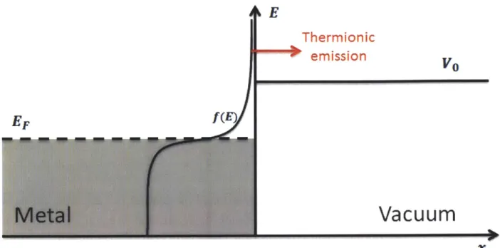
Thermionic emission
f(E
Fig. 2.1. Schematic for thermionic emission from metal to region represents the free electron gas. EF is the Fermi level
vacuum. The shaded and VO is the vacuum energy level. Electrons in a metal have a Fermi-Dirac distribution f(E). At a finite temperature, some electrons have energy higher than the vacuum energy level and can be emitted into vacuum.
The thermionic current density in this model is
If
- * f (:_d0 2 0)
dkz rodkx 1
27 w 27 k e(E(k)-EF)/kBT + 1
where gs is the spin degeneracy and ko is the minimum value of kx required for an electron to escape from the metal. For energies well above the Fermi level, the Fermi-Dirac distribution can be approximated by the Boltzmann distribution:
f(E) = e-(E-EF)kBT (2.4)
And for a free electron gas,
hz1k1z
E(k) = 2m
2m
So the minimum x-directed momentum for an electron to escape is
2mVO h2 (2.5) (2.6) 6 E
Vacuum
x
EF VO (2.3)And velocity
vx (k) = hk (2.7)
Therefore, the integral in equation (2.3) can be readily evaluated as em
em =(kBT)2e -(Vo-EF)/kBT
2wr2h3 (28
Note the work function of the metal is defined as
ID = VO -EF (2.9)
Equation (2.8) can be re-written as
j = AoT 2e-/kBT (2.10)
which is the well-known Richardson-Dushman equation, and AO is termed as the Richardson constant.
It can be easily seen that the thermionic current density increases drastically with increasing temperature of the emitter, and the Richardson constant is a material-dependent parameter determining which material is appropriate for thermionic emission applications. Thermionic electron emission guns are usually made of materials like W, LaB6 and ZrO/W, because of their large Richardson constants
and high melting temperature. Thermionic emitters are usually enhanced by the Schottky effect which will be discussed in the following section.
2.1.2 Static Field Emission
Static field emission refers to the phenomenon of electron emission from materials when an electrostatic field is applied. The emission mechanism can be explained by the quantum tunneling effect. Again, we consider a metal with the band diagram as shown in Fig. 2.2. In contrast to the situation shown in Fig. 2.1, the vacuum energy level in Fig. 2.2 is bent down from VO to VO - eEOx by the electrostatic field EO (note both energy and electric field were denoted with E; to avoid ambiguity, we use EO to represent the electric field in this section). The resultant vacuum energy barrier has a triangular shape and electrons can tunnel through this barrier, forming a static field emission current. In static field emission, electrons do not need to gain extra energy to overcome the work function barrier and emission can happen at temperature T = OK. Therefore, static field emission is also termed as "cold" field emission.
f (E) h E Vo - eEOx Static field emission
Vacuum
xFig. 2.2. Schematic for static field emission from metal to vacuum. The shaded region represents the free electron gas. EF is the Fermi level and VO is the vacuum energy level. Electrons in a metal have a Fermi-Dirac distribution f(E). The applied electrostatic field EO bends down the vacuum energy level from VO to VO - eEox. Hence, a triangular vacuum barrier is formed. Electrons can tunnel through this vacuum barrier and lead to static field emission.
We assume the temperature of the metal is 0 K, and according to Fermi-Dirac distribution, all states below the Fermi level are filled while all state above the Fermi level are empty. Within the WKB approximation, the tunneling probability is
T(Ex) = exp[-2 fX2 2m
f (X 2 )1/2 [V(X)-- EX]1/2dx]
x1
where the x-directed electron kinetic energy
(2.11)
(2.12) h 2k 2
Ex = - X 2m
For a triangular barrier, assuming the tunneling electrons are in the narrow range around the Fermi level, thus
2m )1/2(E - EF) (2.13) T(Ex) To exp[2( -2 eE with 4 2m q3/2 To = exp[- -2/h- )/ 2 -] (2.14) 3 eEO
The total tunneling current is
k, dkz dkxehkx
9=
-gsf (Ex)f(E) (2.15)
Considering the Fermi-Dirac distribution at 0 K, f(E) can be suppressed and the
integral is over a sphere with radius kF - 2mEF in k-space. Also, we neglect the
negative sign as the direction of the emission current is always pointing into the material so we are only interested in its magnitude. Finally, we arrive at the Fowler-Nordheim equation which correlates the electron emission current density with the local electric field and the material work function:
e3E2 8wVdic 3/2
= 3wh2exp[- 3hE (2.16)
87rhO 3heE
where J is the electron emission current density, h is Planck's constant, m is the mass of the electron, c is the work function of the emission material, e is the charge of the electron and E is the local electric field at the emission region (since the energy of the electron is no longer explicitly shown, we switch back to E as the denotation of the electric field).
In reality, the vacuum potential barrier is not perfectly triangular. The local electric field can round the top of the triangular potential barrier and reduce the height of the barrier, known as the Schottky effect:
cDeff = 0 - e[eE/(4wE0) 1/2 (2.17)
where (Deff is the effective barrier height, cD is the original barrier height, e is the charge of the electron and E is the local electric field at the emission region.
When applying a static field to thermionic electron guns, the Schottky effect can reduce the effective work function and hence increase the thermionic emission current. The resultant emitters are termed as thermal Schottky guns or thermal field
emission (TFE) guns, in contrast to cold field emission guns relying on pure field emission.
As with static field emission guns, the electrostatic field is always present. Moreover, the image force potential induced by the image charge can also modify the shape and height of vacuum potential barrier. All of these effects lead to a modified form of Fowler-Nordheim equation [30]:
e3E2 81
N/ D3/2
8ht2(W) [ h v(w)] (2.18)
where v(w) is a slowly varying function taking into account the image force of the tunneling electron with 0.4 < v(w) < 0.8, and the value of function t(w) is approximately 1 with w = e 3/2 (E/4weO)1/ 2/D.
2.1.3 Photoelectron Emission
Photoelectron emission is the electron emission induced by incident photons. The photo-electric effect, discovered by Einstein more than a hundred years ago, is the first demonstration of photo-electron emission. However, the complexity of the photo-electron emission physics is not fully revealed until recently [8-15].
Photo-electron emission can be further divided into optical field emission and single-/multi-photon emission, both illustrated in Fig. 2.3. Due to different operating regimes, optical field emission and single-/multi-photon emission are observed. For optical field emission, the electrons are ripped off from emitters by the electric field of the incident laser; or equivalently, the electrons tunnel through the emitter-vacuum potential barrier assisted by the electric field of the laser pulse. For single-/multi-photon emission, the electron absorbs one or more photons of the laser, hence gaining enough energy to overcome the work function barrier, followed by over-the-barrier emission. Whether the emitters are operating in the optical field emission regime or single-/multi-photon emission regime depends on the drive laser power. For low laser power, single-/multi-photon emission dominates, while for high laser power, optical field emission supercedes. The existence of a strong DC electric field comparable to the optical field also assists the transformation from single-/multi-photon regime to optical field regime [10]. The Keldysh parameter [31] provides a quantitative method to determine the operation regimes. The Keldysh parameter y is calculated by
y = /eE /(2m(b) (2.19) where o is the angular frequency of the incident light, m is the mass of the electron, (P is the work function of the emission material, e is the charge of the electron and E is the local electric field at the emission region. For y
>>
1, single-/multi-photon emission makes the major contribution, while optical field emission dominates for y«
1. For y ~ 1, the photo-induced electron emission is in the transition regime between single-/multi-photon emission and optical field emission.E Multiphoton ---hv --- emission E F --- ~hv --hv Optical field emission VO - eEOcos(wt)x
Vacuum
xFig. 2.3. Schematic for optical field emission and multiphoton emission from a metal to vacuum. The shaded region represents the free electron gas. EF is the metal Fermi level and VO is the vacuum energy level. Electrons in a metal have a Fermi-Dirac distribution f(E). The applied optical field Eocos(wt) bends the vacuum energy level up and down from VO to VO - eEOcos(wt)x. For optical field emission, the electron tunnels through the vacuum barrier when the optical field bends down the vacuum energy level and thins the barrier. For multiphoton emission (three-photon emission in the figure), the electron absorbs multiple photons so that it gains enough energy to overcome the work function barrier. For single-/multi-photon emission, since the electron needs to absorb n photons simultaneously to overcome the work function barrier, the electron emission current density is proportional to the nth power of the incident laser intensity:
and hence proportional to the (2n)th power of the incident laser field:
J oc (E)2n (2.21)
where n is the number of photons required for an electron to overcome the work function barrier:
nhw ! cD (2.22)
The probability of photon absorption also depends on polarization and reaches a maximum when the incident electric field is polarized perpendicular to the surface
[11]. Thus, equation (2.21) can be modified to
J oc (Ecos6)2n (2.23)
where 6 is the polarization angle of the incident light, with 6 = 0 indicating the electric field is polarized perpendicular to the emission surface.
For optical field emission, on the other hand, the electrons are emitted via quantum tunneling effect. The electric field of incident light can be treated as a harmonically oscillating field which bends the vacuum energy level up and down. When the vacuum level is bent down, namely the electric field is pointing inside the material,
a triangular potential barrier is formed and electrons can tunnel through this barrier. Therefore, the Fowler-Nordheim equation (2.18) is still applicable for optical field emission, as long as the static field in the equation is substituted by a harmonically oscillating field.
The above discussions did not present a complete and accurate theoretical treatment of photo-electron emission. However, the physical picture is clear and the theory is enough to guide the design of optical field emitters and interpret experimental results qualitatively and quantitatively. The most important result is that increasing the local electric field (near-field) strength can greatly improve the photo-electron emission yield. This is explicit for optical field emission, where the
emission current density can be calculated from the Fowler-Nordheim equation
J
= AE 2exp(-B/E) (2.24)where A and B are material dependent constants. The emission current density is dramatically increased with increasing near-field. This is also valid for single-/multi-photon emission. The probability for the material to absorb n photon is proportional to the nth power of local intensity and hence the (2n)th power of local
Pabs C (I)n c< (E)2n (2.25)
Thus, a strong near-field will result in increased absorption probability and hence increased single-/multi-photon emission yield. This indicates that the analysis of the non-linear process of photoelectron emission can be decoupled into two steps: first calculation of the near-field and then calculation of the photo-electron emission current or yield. Near-field calculations can be done by solving Maxwell's equations, as discussed in the next section, while electron emission can
be analyzed with the theory discussed in this section.
2.2 Electromagnetics Theory
2.2.1 Maxwell's Equations
Electromagnetic problems can be solved via the Maxwell's equations:
Faraday's Law V X E = or E-ds= - - -da (2.26)
at fc fs a t
Ampere's Law V x H = +J or H - ds = ( +J) -da (2.27)
a t fc fs at
Electric Gauss's Law V -D = p or
f
D-da= ff pdV (2.28)Magnetic Gauss's Law V - B = 0 or B - da = 0 (2.29) Here, both the differential and integral forms of the equations are shown.
We are particularly interested in the situation in which the fields vary time-harmonically, namely, at a single frequency. This is because in the frequency domain, the time derivatives can be replaced by simple multiplication. Also, according to Fourier's theorem, an arbitrary electromagnetic wave can be represented as the superposition of time-harmonic waves with different frequencies. Moreover, the material properties usually have a frequency dependence, while their time-dependent response is usually less clear. Solving Maxwell's equations in
frequency domain is a more natural and accurate approach.
In frequency domain, phasor notation is introduced for electromagnetic fields. For example,
E(r, t) = Re[E(r)e"] (2.30) where the complex vector E(r) is the phasor of time-dependent electric field
E(r, t). Hence, Maxwell's equations become complex in frequency domain:
V x E = -jwB (2.31)
V x H =joD
+j
(2.32)V -D = p (2.33)
V - B = 0 (2.34)
2.2.2 Wave Equation
Combining Faraday's and Ampere's laws, the following equation can be derived:
V x V x E + yE E = 0(2.35)
And for piecewise homogeneous media, equation (2.35) can be reduced to 02
V2 E-ipE jy2 E= 0 (2.36)
Equations (2.35) and (2.36) can also be written in the frequency domain:
V X V E - O 2MEE = 0 (2.37)
V2E + W2pEE = 0 (2.38)
Equations (2.35), (2.36), (2.37) and (2.38) are all widely used forms of the wave equation, which describes the propagation of electromagnetic waves. Take equation (2.38) and assume a frequency-dependent wave vector k(w) , the
following equation can be derived
k(W) 2 =W2 E (2.39)
This equation characterizes the dispersion relation of the medium in which the electromagnetic wave is propagating.
2.2.3 Boundary Conditions
Electric and magnetic fields at a boundary between two media have to satisfy certain boundary conditions. By applying the four Maxwell's equations to an infinitesimal region across the boundary, the following four boundary conditions can be obtained:
n x (E1 - E2) = 0 (2.40)
n - (D1 - D2) =Ps (2.42)
n -(B1 -B 2) = 0 (2.43)
where J, is the surface current density, ps is the surface charge density, and subscripts 1 and 2 indicate field components in medium 1 and medium 2, respectively. In other words, the boundary conditions require: (i) tangential electric field E is continuous across the boundary; (ii) tangential magnetic field strength H changes values at a boundary in accordance with the surface current density; (iii) normal electric displacement field D changes values at a boundary in accordance with the surface charge density; and (iv) normal magnetic field B is continuous across the boundary.
It is interesting to look at equation (2.42), the boundary condition resulting from electric Gauss's law. For a perfect conductor, the fields within the conductor are zero. Hence,
n-Di = ps (2.44)
In other words, the surface charge density is the normal electric displacement field.
If we define surface (electric) field as the (electric) field normal to the interface
between a prefect conductor and a dielectric, then the surface charge density is proportional to the surface field. For non-perfect conductors, such as gold in optical frequency, this proportionality relation still holds as a reasonably good approximation. This relation between surface charge density and surface field for conductors is very important. In numerical simulations, the charge distribution can be difficult to determine as its calculation involves taking derivatives of the fields and huge numerical artifacts caused by discontinuous values of the fields can emerge. In this situation, the calculation of surface fields provides an easier way to investigate the charge distribution.
2.2.4 Constitutive Relations and Material Properties
Constitutive relations are
D =EE (2.45)
B = H (2.46)
Permittivity E and permeability p reflect the electromagnetic properties of materials. The ratio of the material permittivity (permeability) to vacuum permittivity (permeability) is called relative permittivity (permeability). Since the
vacuum permittivity and permeability are physical constants, E and [t are sometimes used as notations for relative permittivity and permeability without ambiguity.
At optical frequency, the permeability is usually the same as its value in vacuum except for some engineered metamaterials. However, the permittivity is quite different from its value in vacuum and determines materials' response to optical waves.
2.2.5 Quasi-Static Approximation
One consequence of the Maxwell's equations is that changes of charges and currents in time are not synchronized with changes of electromagnetic fields, which are often delayed due to the finite speed of electromagnetic wave propagation. This is called the retardation effect, which usually complicates the analysis of problems. Also, solving Maxwell's equations usually requires intensive computation efforts. In certain kinds of problems, approximations can be made to simplify the equations. One of the most frequently encountered situations is electrostatics (magnetostatics), where the electric (magnetic) field is static or oscillating at a very low frequency. Hence, the electromagnetic wavelength is so large that the phase shift or phase gradient is caused only by inductive or capacitive material properties rather than by wave propagation delays. Therefore, quasi-static approximation can be applied, where the retardation effect and phase shift due to wave propagation can be safely neglected. As a result, for electrostatic problems only the electric Gauss' law needs to be considered and Maxwell's
equations are reduced to
V - (EE) = p (2.47)
where p is the charge density and E is the electric field, satisfying
E = -V (2.48)
where Cj is the electrostatic potential. If the medium is piece-wise homogeneous,
the above equation can be further rewritten as the famous Poisson equation:
V2p = -p/E (2.49)
and it yields the Laplace equation in a charge-free region of space:
Before applying the quasi-static approximation, its validity should be carefully reviewed. In general, it is valid if the electromagnetic wavelength is ten times larger than the spatial dimension of the problem. The longer the wavelength, the higher accuracy the approximation possesses. The interaction between light and subwavelength structures can usually be analyzed with the quasi-static approximation. For the extreme situation where the electric field does not change with respect to time, the approximation becomes the exact representation.
2.2.6 Nano Optics
Nano optics refers to the study of interactions between light and nanoscale objects. It has been under heated investigation recently thanks to the development of nanofabrication methods, numerical computation power and optical techniques. According to the Heisenberg uncertainty principle,
h
A(hk)Ax > - (2.51)
2
where Ax and Ak are the spatial and momentum spread of a photon, respectively. The maximum momentum spread is the free space wavevector [32]
k = 27r/A (2.52)
Thus, the maximum spatial spread is
Ax >- (2.53)
47
This is one form of the well-known diffraction limit of light, telling that the spatial confinement of optical energy (e.g. light focused by a lens) cannot be smaller than a certain fraction of its wavelength. However, this limit can be broken by near-field light, of which the wavevector can be decomposed into a transverse component and a propagating component:
k= kI + k (2.54)
For light interacting with subwavelength structures with a dimension much smaller than wavelength and hence below the diffraction limit, the transverse wavevector is larger than the free space wavevector:
Combining (2.54) and (2.55), the propagating wavevector can only be imaginary:
kl = ia (2.56)
Therefore, the light cannot propagate away from the subwavelength structure, hence the name "near-field".
Light has a wavelength ranging from several hundred nanometers to a few micrometers while nanostructures usually have a sub-100 nm dimension. As a result, the interactions between light and nanoscale objects, or nano optics, are essentially the interactions between subwavelength structures and near-field.
2.3 Surface Plasmon Resonance
Surface plasmon resonance (SPR) is the collective oscillation of electrons in a solid stimulated by incident light. The resonance condition is established when the frequency of light photons matches the natural frequency of surface electrons oscillating against the restoring force of positive nuclei. The study of surface plasmons, plasmonics, is an important sub-area of nano optics as it usually involves the evanescent field (near-field) or light interacting with subwavelength nanostructures, and one important feature of surface plasmon resonance is its capability of confining electromagnetic energy to subwavelength dimensions.
Plasmonics contains two main components, surface plasmon polariton (SPP), originating from the work of Sommerfeld [33] and Zenneck [34] on surface waves propagating along the surface of a finite conductor, and localized surface plasmon resonance (LSPR), originating from the work of Mie [43] on light scattering by metallic particles.
2.3.1 Electromagnetic Properties of Metals
Most of the materials exhibiting SPR are metals, so it is important to first understand the electromagnetic properties of metals.
We start by considering a homogeneous free electron gas responding to a harmonically oscillating electric field E = E0e0t [32]:
a2r
where m is the mass of electron, e is the charge (absolute value) of an electron and r is the position of the electron.
The solution of equation (2.57) gives
e
r = 2 E (2.58)
Moreover, the macroscopic polarization caused by the displacement of free electron gas is
P = -ner (2.59)
where n is the number of electrons per unit volume. Thus,
ne
2P = - E (2.60)
mW2
Recall that polarization can be expressed as
P = EOX(O)E (2.61)
where X(w) is the frequency-dependent electric susceptibility relating to (relative) permittivity or dielectric function E by
E(W) = 1 + X(W) (2.62)
Combining equations (2.60), (2.61) and (2.62), the permittivity of free electron gas is
W2
= 1-P (2.63)
where wp is the free electron gas plasma frequency defined as
ne 2
p (2.64)
jMEO
By using the Drude model, which treats the metal as a free electron gas, equation (2.63) is thus the frequency-dependent permittivity of the metal.
It is interesting to further discuss equation (2.63) as the metal permittivity. At frequency below the plasmon frequency (w < wp ), the metal permittivity is negative (e(o) < 0). According to the dispersion relation given by equation (2.39),
the wave number is purely imaginary, namely, electromagnetic wave cannot propagate within the metal. This is the exact reason that metals can be treated as
perfect conductors and are usually used as the materials for mirrors and waveguides at low frequencies. On the other hand, at frequencies above the plasmon frequency (w > op), the wave number is positive and the metal becomes transparent for high frequency electromagnetic waves.
When an electron is oscillating in a metallic solid, scattering by ion cores can cause damping of the oscillation. We can also include the damping effect into the Drude model and modify equation (2.57) as
a2r Or .
m + m7 - = -eEoefwt (2.65)
at 2
at
where the second term on the L.H.S. characterizes the damping effect. With the same approach, metal permittivity can be written as
02
c(w) = 1 - 2 (2.66)
0)2 + jrfo
Now the permittivity possesses an imaginary part which corresponds to the damping or absorption effect of electromagnetic waves.
The Drude model is reasonably accurate as long as the metal can be approximated as a free electron gas. However, at high frequencies, interband transitions arise and the Drude model permittivity deviates from experimental data. In this situation, the more accurate Drude-Lorentzian model should be used:
a2r Or
m - + mE- + mWOr = -eEoe Jwt (2.67)
Ot 2 Ot
The third term, a harmonic oscillating term, is added on the L.H.S. This is because interband transitions involve valence electrons which are bound to the ion cores so that they can be modeled by a Lorentzian oscillator, oscillating with respect to the cores. The permittivity is thus
2
E(W) =) (2.68)
In fact, the (Drude-)Lorentzian model is a more generalized model compared to the free electron Drude model, and it can also be used to model the permittivity of dielectric materials and not merely metals.