HAL Id: hal-01412585
https://hal.archives-ouvertes.fr/hal-01412585
Submitted on 12 Dec 2016HAL is a multi-disciplinary open access
archive for the deposit and dissemination of sci-entific research documents, whether they are pub-lished or not. The documents may come from teaching and research institutions in France or abroad, or from public or private research centers.
L’archive ouverte pluridisciplinaire HAL, est destinée au dépôt et à la diffusion de documents scientifiques de niveau recherche, publiés ou non, émanant des établissements d’enseignement et de recherche français ou étrangers, des laboratoires publics ou privés.
Copyright
Cathodoluminescence spectroscopy of plasmonic patch
antennas: towards lower order and higher energies
Mathieu Jeannin, Névine Rochat, Kuntheak Kheng, Gilles Nogues
To cite this version:
Mathieu Jeannin, Névine Rochat, Kuntheak Kheng, Gilles Nogues. Cathodoluminescence spec-troscopy of plasmonic patch antennas: towards lower order and higher energies. Optics Express, Optical Society of America - OSA Publishing, 2017, 25 (5), pp.5488. �10.1364/OE.25.005488�. �hal-01412585�
Cathodoluminescence spectroscopy of plasmonic patch antennas:
towards lower order and higher energies
Mathieu Jeannin,1, 2 Névine Rochat,1, 3 Kuntheak Kheng,1, 4 and Gilles Nogues1, 2 1Univ. Grenoble Alpes, F-38000 Grenoble, France
2CNRS, Inst. NEEL, "Nanophysique et semiconducteurs" group, F-38000 Grenoble, France 3CEA, LETI, MINATEC Campus, F-38054 Grenoble, France
4CEA, INAC, "Nanophysique et semiconducteurs" group, F-38000 Grenoble, France
Abstract
We report on the cathodoluminescence characterization of Au, Al and a Au/Al bimetal circular plasmonic patch antennas, with disk diameter ranging from 150 to 900 nm. It allows us access to monomode operation of the antennas down to the fundamental dipolar mode, in contrast to previous studies on similar systems. Moreover we show that we can can shift the operation range of the antennas towards the blue spectral range by using Al. Our experimental results are compared to a semi-analytical model that provides qualitative insight on the mode structure sustained by the antennas.
I. INTRODUCTION
Advances on classical and quantum solid state light emitters and optoelectronic devices bring great interests in controlling light emission properties of nano-sized emitters. As an example, several approaches are employed in the field of semiconducting quantum dots, from microcavities1 and other photonic structures2–4 to plasmonic antennas5–8. In the latter case, a great effort has been made to develop new antenna geometries that could increase the coupling strength between a single emitter and the antenna. Additionally, researchers are investigating novel possibilities of controlling the radiation pattern of the coupled structure. One of the emerging strategies is to confine the plasmon field inside an insulating layer comprised between a metallic nanoparticle and a continuous metallic film. Such structures were initially investigated using colloidal plasmonic particles9,10. Due to the strong electric
field enhancement possible inside the insulating layer, these systems were soon proposed as promising plasmonic cavities. Recent demonstrations include a 1900-fold increase in emission intensity for colloidal quantum dots11, and reaching up to the strong coupling regime for
single molecules placed between colloidal Au spheres and an Au mirror12. All of these systems rely on the coupling between the dipolar localized surface plasmon mode supported by the nanoparticle and the metallic mirror. Another key properties of the particle-on-a-mirror geometry is that the coupling between the plasmon mode supported by the particle and the film allows to dramatically change the emission diagram of the coupled system. This was especially investigated using Au disk antennas on a Au mirror. Because of geometrical and electric field profile similarities to their radio-frequency counterparts, these laterally confined insulator-metal-insulator-metal (IMIM) nanostructures were then designated as plasmonic patch antennas13–15. They have been successfully coupled to colloidal quantum dots16 and studied by cathodoluminescence17. Contrary to the nanoparticle-on-a-mirror experiments,
circular patch antennas reported up to now have large diameters. They can be thought as circular cavities for surface plasmon polariton modes. Their large size and subsequent large number of supported mode is the key to the control of their radiation pattern.
In this article, we use cathodoluminescence (CL) spectroscopy and imaging on Au and Al circular plasmonic patch antennas in the intermediate regime between large antenna and small particle. We characterize circular antennas supporting single mode operation as well as highly multipolar modes. The CL signal collected from plasmonic antennas is closely
related to the electromagnetic local density of states (LDOS). In17–19, it is shown that the signal measured in CL corresponds to the integration over the electron beam path of the partial, radiative LDOS projected along the electron beam path. It allows to precisely characterize the antennas, to determine their spectral properties and to map the radiative LDOS on a nanometer scale for each antenna resonance. The paper is organized as follows: we first present the patch antennas fabrication and the CL system. We then introduce the fundamental properties of Au patch antennas and a semianalytical model proposed to explain their mode structure14,17. We then study antennas of smaller dimensions, down to ∼170 nm
in diameter, allowing for the study of the fundamental antenna mode. Finally, using Al patch antennas we demonstrate that changing the antenna material makes it possible to shift their operation range down to a wavelength of 450 nm. Indeed, Al is seen as a promising candidate for blue and U.V. plasmonics20–23 in spite of the current low quality of Al films24. It has the additional advantage to be compatible with current CMOS fabrication technologies, easing a possible large-scale implementation of Al-based plasmonic devices.
II. SAMPLE FABRICATION AND EXPERIMENTAL DETAILS
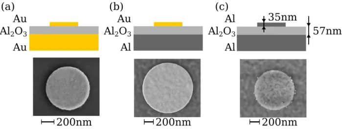
Figure 1. Sketch of the three patch antennas configurations: (a) Au patch and Au mirror, (b) Au patch and Al mirror, and (c) Al patch and Al mirror. In each case, the Al2O3 spacing layer thickness is 57 nm. Below each sketch, we show an SEM image of a typical antenna. Notice the difference in surface roughness from (a) to (c) due to the poor quality of the thick Al film.
(Au or Al, 100 nm) is evaporated on the substrate using e-beam evaporation. In order to get the best optical properties, we aimed at lowering as much as possible the surface roughness and granular structure of the films. Au evaporation is performed under ∼ 10−6 mbar at an evaporation rate of ∼ 2 Å/s. Al has a tendency to oxidise a lot more easily than Au, and therefore smooth Al films are hard to obtain with the vacuums levels available in conventional e-beam evaporation machines. A possible way to improve the quality of the film is to use a higher evaporation rate, in our case 2 nm/s24. The spacing oxide layer is then deposited using atomic layer deposition, and its thickness is controlled using an interferometric measurement after deposition.
All the top layer plasmonic structures are fabricated by electron beam lithography. An electron-sensitive, positive resist (Poly(metyl methacrylate), or PMMA) is spin-coated on the sample and soft-baked on a hot plate at 180◦C for 5 min. The disks are patterned using an electron beam exposing the resist upon electron impact. Each disk is separated from its neighbours by a distance greater than 2 µm to avoid any coupling between two adjacent structures. The resist is then developed, and 35 nm of metal (Au or Al) is deposited using electron gun evaporation. A final lift-off process is performed in 1-methyl-2-pyrrolidinone (NMP) heated at 80◦C to remove the remaining resist.
Three IMIM systems are under investigation. In each case, the Al2O3oxide layer thickness
is 57±2 nm. First, Au patch antennas were fabricated on an Au mirror, as shown in Fig. 1(a), with diameters ranging from 280 to 900 nm. Second, Au patch antennas on an Al mirror were fabricated with diameters ranging from 120 to 930 nm (Fig. 1(b)). Finally, Al antennas on an Al mirror were fabricated, with diameters also ranging from 120 to 930 nm (Fig. 1(c)). As can be seen in the scanning electron microscope (SEM) images in Fig. 1, the Au deposition results in a very smooth Au film and antenna surface. Magnified SEM images revealed an Au grain size of around 10 nm. The Al film appears a lot rougher, as can be inferred from Fig. 1(c). We noticed that Al grains tend to coalesce, so the smoothness of the top surface degrades upon increasing the deposited thickness. Hence, the top surface of the Al mirror (100 nm thick) shows Al grains sizes of around 40 nm, and is a lot rougher than the Al antenna surface (35 nm thick) which has Al grains of only 20 nm in size. Note that in the case of bimetal antennas the roughness of the Al film also slightly degrades the quality of the Au top disk, as seen in Fig. 1(b).
Our cathodoluminescence setup consists in FEI (quanta 200) SEM fitted with a drilled
home made asymmetric parabolic mirror allowing for electrons to pass through, and provid-ing a very large numerical aperture (NA) rangprovid-ing from 0.5 (detector side) to 0.9 (parabola side). We use an acceleration voltage of 30 keV and a beam current around 7 nA. The hole allowing for the electrons to pass is 500 µm in diameter, preventing light collection in the vertical direction with an angular divergence of a few degrees. The CL signal collected by the mirror is focused on the entrance slit of a spectrometer (Horiba Jobin-Yvon IHR550) by a spherical mirror, preventing chromatic aberrations. The light is then dispersed by a 150gr/mm grating blazed at 550 nm and sent either to a charged-coupled device (CCD) camera (Andor Newton) or energy-filtered through the exit slit of the spectrometer and sent to an avalanche photodiode (APD) to obtain energy-selective CL images.
Complementary experiments were carried out using a Attolight commercial Rosa CL setup allowing for hyperspectral imaging. The electron beam acceleration voltage is 10 keV, with a beam current of 25 nA. The light is collected using a Cassegrain-type objective (NA 0.72) embedded inside the electronic column of the scanning electron microscope. The collected light is focused on the entrance slit of a spectrometer (Horiba Jobin-Yvon IHR320), dispersed using a 150gr/mm grating blazed at 500 nm, and detected using a CCD camera (Andor Newton).
III. CATHODOLUMINESCENCE OF AU PATCH ANTENNAS
Let us first describe the spectral properties of the Au patch antennas. To obtain the antennas CL spectrum, we raster scan the electron beam over the antenna surface, using a square scanning area exactly circumscribing the disk. The beam scanning time is set to be much smaller than the integration time (∼1 min) so that every point on the antenna surface can be considered as equally excited. A background spectrum is acquired by scanning the exact same area on a region where no antenna is present, recording the CL response of the bare substrate. This substrate spectrum is subtracted from the antenna’s CL response. We note that the background luminescence from the substrate has an intensity of ∼ 4000 s−1, while the CL signal originating from localized surface plasmon modes supported by the antenna is ∼ 20 s−1 in intensity. The background subtraction procedure does not suppress entirely the contribution of the substrate luminescence to the collected CL signal. A typical antenna spectrum is presented in Fig. 2(a) (590 nm diameter). It presents a broad peak
Figure 2. (a) Typical CL spectrum of a Au patch plasmonic antenna of 590 nm diameter. The background contribution is shown in red dashed line. The LSPRs of the antenna are indicated, with the Roman number corresponding to the LDOS images in panel (b) and branches in panel (d). (b) Corresponding energy-filtered CL images revealing the LDOS pattern associated with the first six resonances branches in (c). The yellow circles represent the antenna physical size. (c) Waterfall plot of the CL spectra obtained for different antenna diameters. The red lines follow the position of the resonances (marked in black) and serve as guides for the eye. They are numbered from the lowest order (smallest antenna) to the largest order in small Roman numbers. (d) Corresponding intensity color-coded spectral map of the antennas CL signal as a function of wavelength and antenna diameter. The resonance branches are evidenced in green lines as guides for the eye, with the same Roman numbering. Note that we have fixed the width of each spectrum, resulting in an unevenly spaced vertical scale, to better show each resonance position. The black dashed line corresponds to the spectrum in (a).
indicated in red dashes. This signal comes from residual luminescence due to Au interband transitions for wavelengths below 600 nm25 as well as from the diffraction by the patch edge
of the surface plasmon polaritons excited outside the antenna region at larger wavelength. Sharper peaks are visible at 650 and 750 nm, which we attribute to localized surface plasmon resonances (LSPR) of the antenna. CL images of the LDOS corresponding to each LSPR are obtained by slowly scanning the electron beam over the antenna surface, collecting the light emitted in a 50 nm spectral bandwidth around the resonance. This filtered CL emission is then detected by an APD and correlated to the electron beam position. The spectral integration bandwidth is selected to maximise the collected intensity, matching the resonance bandwidth but ensuring that we collect only light emitted from a single resonance. In the rest of the article, the LDOS images are normalized in intensity. The typical emission probability is of the order of 10−6 photons per incident electrons. More information on the LDOS image acquisition is given in the Appendix section. Note that the CL images do not reveal the antenna mode structure, but rather map the probability of exciting a given antenna mode at each electron beam position. The LDOS images corresponding to the two LSPR peaks observed in Fig. 2(a) are shown in the corresponding iv and v insets in Fig. 2(b). We subsequently repeat this procedure for several antenna diameters, and obtain the antenna spectrum with its LSPR peaks and their corresponding LDOS patterns. In Fig. 2(c), we gather all the antenna spectra in the form of a waterfall plot. The experimentally measured antenna diameters are indicated, and fabrication imperfections are responsible for the non-even spacing between the different antennas sizes. It is also represented by the color-coded intensity spectral map in Fig. 2(c) which represents the CL spectra as a function of wavelength and increasing diameter. Note that the vertical scale has a fixed width for each spectrum. This representation will be used again in Fig. 6.
The LDOS imaging allows us to track a given LSPR with respect to the antenna diameter change. It reveals that the successive LSPRs of the patch red-shift with increasing antenna diameter. The red-shifting resonances branches are marked with red solid lines serving as guides for the eye. All the resonances belonging to a given branch show the same spatial structure, as represented in Fig. 2(b) for the first six branches. Each pattern is composed of one or more concentric rings. In addition, considering successive LDOS patterns (from i to vi) we observe an alternation of bright and dark antenna center, in agreement with previous reports17. Furthermore, we do not observe any azimuthal dependence of the LDOS. This
will be discussed in the modelling section.
IV. SEMI-ANALYTICAL MODEL
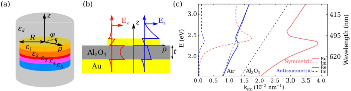
The optical properties of plasmonic patch antennas can be described by the semi-analytical model of ref.17 which is adapted from the fully analytical work of ref.14. The analytical model considers an arbitrary stack of circularly symmetric layers of fixed radius R, different thickness tj and permittivity εj, where j is the layer number, embedded in an
homogeneous medium of permittivity εd. A sketch of the geometry is shown in Fig. 3(a).
The stack is considered as a circular cavity supporting Bessel-type surface plasmon polariton (SPP) modes. The dispersion relation of the different SPP modes and their vertical mode profile are numerically calculated from the equivalent infinite (R → ∞) multi-layer system26. In the case of our insulator-metal-insulator-metal (IMIM) geometry, only two distinct prop-agating SPP modes are present, referred to as symmetric and antisymmetric due to the symmetry of the Ez component of the electric field. The vertical profiles of Ez are sketched
in Fig. 3(b) in red (symmetric mode) and blue (antisymmetric mode). The symmetric mode has most of its energy confined inside the spacing layer, while the antisymmetric mode is rather confined at the top air/metal interface. The respective dispersion relations of the two modes are presented in Fig 3(c), where the solid lines represent the real part of the dispersion relation, and the dashed lines its imaginary part. The antisymmetric mode shows low losses but is almost index-matched with the free-space dispersion relation in air, and is thus poorly confined at the metal surface. The symmetric mode significantly deviates from the free-space propagation in alumina, indicating a strong confinement. It also suffers from greater losses than the antisymmetric one. Because it presents a very strong electric field inside the alumina layer and matches the polarisation of the exciting field created by the electrons, this mode plays a dominant role in the CL experiment. Hence, as in refs.17,27, we
restrict the subsequent analysis to the symmetric vertical mode profile.
The electric field is decomposed into eigenmodes of the circular geometry in which the z, ρ and ϕ dependences can be separated as:
Ezn,m(ρ, z) = a(z)Jm(kn,mρ) exp (imϕ) (1)
Figure 3. (a) Sketch of the geometry considered in the analytical model developed in17. (b) Sketch of the experimental geometry, with the two vertical mode profiles sustained by the patch antenna: symmetric (red) and antisymmetric (blue). Note that in our case, only the patch is of finite radius R. (c) Dispersion relations of the symmetric (red) and antisymmetric (blue) mode profiles. The real part of the wave vector kn,m is represented in solid lines, and its imaginary part in dashed lines. The black dashed lines are the photonic dispersion relations in air and alumina.
where a(z) is the vertical mode profile sketched in red in Fig. 3(b), Jm is the Bessel function
of the first kind of azimuthal order m, ρ is the radial vector and kn,m is the surface plasmon
polariton wave vector supported by the infinite multilayer structure following the dispersion relation of Fig. 3(c). The eigenfunctions are further determined by the resonance condition:
Re [kn,m] 2R + ϕm = 2xn(Jm) (2)
where Re [kn,m] denotes the real part of the SPP wave vector. The phase factor ϕm accounts
for the phase shift acquired upon reflection at the patch edge ρ = R. xn is the n − th
zero of the Bessel function Jm. While ϕm can be numerically calculated for each azimuthal
number m according to ref.14, we used the empirical formulas and method reported in ref.17
instead. The main approximation is that ϕm is considered the same for all antenna modes
(n, m). Equation 2 gives the resonant frequencies ωn,m of the disk after inversion of the
SPP dispersion relation. The LDOS Γ (ω, ρ) probed during the CL experiment can thus be expressed as: Γ (ω, ρ) ∝X n,m |En,m z (ρ)| 2 L (ω, ωn,m, γn,m) (3)
where the energy of the mode profile Ezn,m(ρ) is normalized in space throughRR 2πρ |Ezn,m(ρ)|2dρdz = 1, and L (ω, ωn,m, γn,m) is a normalized Lorentzian function centred at frequency ωn,m with
a full width at half maximum γn,m so that R L (ω, ωn,m, γn,m) dω = 1. Following ref.17, the
width of the Lorentzian function is given by:
γn,m/ω = (2Im [kn,m])2+ γ0(1 + ωnormb ) −1
(4)
where γ0 and b are adjustable parameters used to fit the resonance bandwidth of the
an-tennas, Im [kn,m] is the imaginary part of the SPP wave vector, and ωnorm = ω/(1800 THz).
The frequency broadening of the antennas resonances describes the loss-induced frequency broadening of the plasmonic patches. Note that as the LDOS is related to the square mod-ulus of the electric field, one can only detect the radial dependence of the plasmon mode, and not its azimuthal dependence.
Using the previous relations we compute the different resonances contributing to the LDOS for each radius of the the fabricated antennas. The fitting parameter ϕm was obtained
in17by matching the resonance of the fundamental antenna mode to the results of numerical simulations. However, due to the large disk size, this mode had a very low energy and could not be experimentally observed. Here instead, we match the position of all the antenna modes with the experimentally determined resonances of branches i, ii and iii in Fig. 2(c). In this case, we find that a correction on the SPP dispersion relation is necessary to reproduce the experimental mode dispersion. The semi-analytical model thus seem to underestimates the mode wave vector by a factor 1.5 to 2. This might be due to the fact that the model considers the disks as cavities for propagating SPPs, whereas for small disks the large lateral confinement may result in larger SPP effective wave vectors, as already described in the case of plasmon waveguides28,29. Fitting the experimental data, we find γ
0 = 0.05, b = 1.7, and
ϕm= 0.5.
Comparing the results of the simulations with the experimentally determined spectra and LDOS reveals further information on the mode structure supported by the patch antennas. Figure 4(a) shows the comparison between the measured spectrum (thick red line) and the predicted resonances (thin lines) for a 270 nm diameter antenna (smallest antenna in Fig. 2(c)). The main contribution to the LDOS originates from the three Bessel modes indicated in thin solid lines, with their radial and azimuthal number (n, m) given in the legend. The simulated spatial LDOS map is shown in Fig. 4(b), while the top insets in panel (a) show the measured LDOS using a spectral bandwidth represented by the shaded area in the spectrum. We can see that the resonance at 750 nm is composed of the (n = 1, m = 2)
Figure 4. (a) Comparison between the measured antenna CL spectrum (thick red line) and the simulated resonances (thin lines) of a 270 nm diameter antenna. The background contribution is indicated in red dashes. The principal Bessel contributions to the simulated spectrum are shown in thin solid lines. The corresponding Bessel numbers (n, m) are indicated in the legend. (b) Simulated spatial LDOS map: as it has no azimuthal dependence, it is represented as the function of the wavelength and the normalized radial coordinate ρ/R which varies form -1 to +1 along the diameter of the antenna. Note the separation between the m = 0 mode producing a maximum of LDOS at the antenna center, and the m 6= 0 modes. (c) Measured CL images using the integration bandwidth indicated by the colored area in (a). The yellow circles indicate the antenna physical size. The Roman numbers refer to the mode branches numbers in Figs. 2(b)–2(c).
and (n = 2, m = 0) modes. The m = 0 modes are the only ones contributing to the LDOS at the antenna center, for symmetry reasons. Note that the m = 0 mode (green) appears at a slightly shorter wavelength than the (n = 1, m = 2) mode (red). On the other hand, the resonance at 650 nm is composed of a single (n = 1, m = 3) Bessel mode. Comparing the spatial LDOS maps with the experimental LDOS images allows us to confirm the fitting parameter.
As noted in17, it is important to realize that the patch antenna resonances are composed of
superposition of several Bessel modes with increasing quantum numbers. This superposition arises from the overlap between the frequency broadened Bessel modes due to ohmic and
radiation losses17. However, in our case, the small size of our patch antenna allows us to image LDOS corresponding to single mode resonances. Doing so, we arrive at a one-to-one correspondence between the LDOS model and the experimental CL images, which was not possible in17. Note that the relative amplitude between the resonances is not reproduced. This is because the model only describes the LDOS supported by the particle, while CL is sensitive to the radiative component of the LDOS. The radiative efficiency and radiation pattern of each resonance is thus left out in the model and is responsible for this discrepancy. Finally, the broad continuum of CL signal below 600 nm is not reproduced by the model, because it is simply due to luminescence from the Au layers and thus not related to the plasmonic mode structure of the antennas.
V. TOWARDS LOWER ORDERS
Figure 4 shows that the antenna can sustain resonances corresponding to a single plasmon mode. Reaching low order mode operation, or even single mode operation is important to efficiently couple the patch antennas to localized emitters placed inside the spacing layer, such as in16. Large patch antennas support a high number of competing mode, which gives them their interesting directional beaming properties, as shown in depth in17. However, a
large radiative enhancement requires a strong coupling between the emitter and a single radiative mode of the antenna. This is why the strongest reported Purcell factors in the patch geometry involve small metallic particles as in refs.11,12. Hence, a trade-off has to be
found between directionality and radiative rate enhancement when coupling nano-emitters to such plasmonic patch antennas.
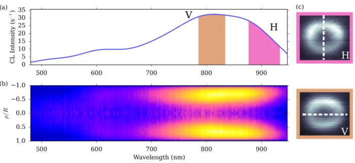
The lowest order radiative mode that can be sustained by the patch antenna is the fun-damental (n = 1, m = 1) dipole-like mode. To reveal this funfun-damental mode, we fabricated smaller Au antennas on an Al mirror. The use of the Al mirror strongly reduces the lu-minescence contribution from the substrate, as will be evidenced in the next section. The CL spectrum and hyperspectral map of the CL signal as a function of the wavelength and antenna reduced radius are presented in Fig. 5 for a 170 nm diameter antenna.
This antenna clearly exhibits a dipole-like LDOS spatial pattern, characteristic of the fundamental (n = 1, m = 1) antenna mode, as can be seen in Fig. 5(b). However, the spec-trum presented in Fig. 5(a) exhibit a very broad unresolved double peak resonance centred
Figure 5. CL spectrum (a) and hyperspectral CL map (b) of a 170 nm diameter antenna. The hyperspectral map in (b) is obtained by summing the spectra of all the pixels whose distance from the antenna center is between ρ and ρ + dρ and normalized to the corresponding surface element. It is symmetric by construction with respect to ρ = 0. It clearly reveals the fundamental antenna mode n = m = 1. (c) LDOS CL image for the spectral integration bandwidths H and V indicated in (a). The degeneracy of the mode is lifted due to the imperfect shape of the disk and lead to the breaking of the circular symmetry. As a consequence we observe a horizontal (H) and vertical (V) splitting of the corresponding LDOS images.
at 845 nm. Using the hyperspectral mode of the setup, we image the LDOS supported by the antenna on the high and low energy side of this resonance. Fig. 5(c) shows the LDOS using the integration bandwidths coloured in Fig. 5(a). It reveals that due to fabrication imperfections, the antenna in not perfectly circular, resulting on an apparent splitting of the fundamental (n = 1, m = 1) mode and breaking of the circular symmetry. We note the the CL signal seems stronger on the upper half of the antenna for both the horizontal (H) and vertical (V) modes in Fig. 5(c). We attribute this effect to the progressive SEM induced contamination of the antenna surface as we scan the beam over it (total acquisition time is ∼30 min)
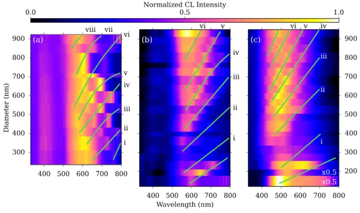
Figure 6. CL intensity spectral maps of Au patch antennas on a Au mirror (a), Au patch antennas on an Al mirror (b) and Al patch antennas on an Al mirror (c) representing the CL spectrum of each antenna as a function of wavelength and diameter. Note that in panel (c), the first two spectra show stronger resonances, and have been divided by 2 to increase the overall contrast. Panel (a) also corresponds to Fig. 2(c).
VI. TOWARDS HIGHER ENERGIES
Having completely characterize the mode structure of small circular Au plasmonic patch antennas, we fabricated Al patch antennas on an Al mirror to extend their operation wave-length to higher energies. Figure 6 gathers the spectral information on patch antennas as a function of patch diameter and wavelength. Panels (a) to (c) correspond to the three different kinds of samples presented in Fig. 1, respectively Au patch on Au film, Au patch on Al film and finally Al patch on Al film. As mentioned previously, the comparison between Fig 6(a) and (b) show that the presence of the Al mirror strongly reduces the luminescence contribution from the substrate, resulting in a low background signal for wavelengths below 550 nm in panel (b). Further comparison between panels (b) and (c) show the dispersion relation of the successive antenna resonances, including the dipole-like, fundamental mode
for small diameters. As seen from Fig. 6(b), the Au patch antennas on an Al mirror pro-vide optical resonances for wavelengths from 550 to 750 nm, while the Al patch antennas in Fig. 6(c) exhibit resonances spanning wavelengths from 450 nm to 650 nm. We note how-ever that there is a trade-off between the vertical confinement of the mode in the oxide layer and the high energy operation of the patch structures. Because most of the energy of the symmetric vertical mode profile is confined inside the oxide layer, increasing the strength of the mode requires a smaller oxide thickness. This leads in return to a stronger confine-ment of the electric field and hence a stronger refractive index sensed by the mode, which results in a red-shift of the resonant wavelengths for a given patch diameter. Furthermore, the plasmonic response of Al particles is limited to the blue and green parts of the visible electromagnetic spectrum, since a broad interband transition is present in Al at 800 nm21.
LDOS imaging experiment on each resonance confirm that the change in material allows to tune the resonant wavelengths of the antennas but does not affect their supported mode structure, which is only characteristic of the antenna geometry. We note that due to the roughness of the Al film, LDOS imaging was more complicated in the case of Al antennas. The presence of such large Al grains produces a lot of parasitic signal arising from surface plasmon modes strongly localized on the grains. Parasitic CL signal also originates from the diffraction by the surface roughness of the continuum of surface plasmon polaritons excited by the electron beam.
VII. CONCLUSION
In conclusion, we have used cathodoluminescence spectroscopy and imaging to investigate the spectral and spatial plasmonic properties of circular plasmonic patch antennas made of Au and Al. In a first step, we have characterized Au patch antennas on an Au mirror. Their characteristic spectrum shows several resonances above 600 nm. Energy-resolved CL imaging allowed us to image the radiative LDOS corresponding to the resonances. We have linked the CL properties of these antennas to a semi-analytical model presented in ref.17. Contrary to what is reported in this reference, we arrive here at a one-to-one correspondence between the measured and simulated LDOS at the expense of correcting the surface plasmon wave vector dispersion relation by an empirical factor. The increasing complexity of the mode structure supported by the antennas comes from the broadening of the modes due to
ohmic and radiation losses. Hence, a single antenna resonance can be composed of several overlapping antenna modes. We then further reduced the size of the circular antennas and used hyperspectral CL imaging to reveal the fundamental mode of Au patch antennas on an Al mirror. Finally, using Al patch antennas on an Al mirror, we demonstrated the possibility to fabricate Al patch antennas providing optical resonances down to 450 nm.
Appendix A: CL System
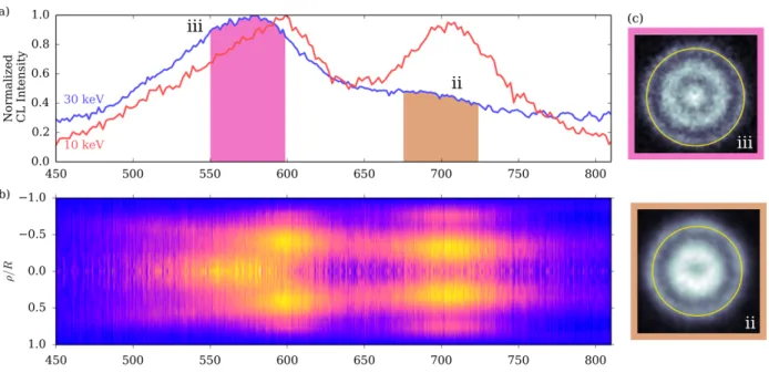
Figure 7. (a) CL spectra for a 435 nm diameter Au antenna on an Al mirror, as presented in Fig 6(b). The red line corresponds to the 10 keV excitation, while the blue line corresponds to the 30 keV excitation. (b) Hyperspectral LDOS imaging with the 10 keV beam as a function of wavelength and reduced antenna radius. (c) LDOS images obtained using the 30 keV setup by integrating the CL signal in the shaded spectral regions. They correspond to the second and third mode branches in Fig. 2(b)–(c), starting from the smallest antenna. The yellow circles indicate the antenna physical size.
To perform LDOS imaging, the CL signal in filtered in energy using the exit slit of the spectrometer and sent on an APD. The APD output is connected to an electronic pulse generator. We ensure that the amplitude and time of the pulse are set so that we operate in a photon counting mode. Typically, the pulse duration is one third of the pause time of the electron beam on each position. The resulting image is thus composed of pixels of discrete
intensity values. A digitalisation step is perform to convert these discrete intensity values into a number of counting events. To account for the spatial extension of the electron beam, a spatial Gaussian filter of 10 nm width is applied on the signal.
We can compare the results obtained from the two CL setups using Fig. 7, where the CL properties of a 435 nm diameter Au antenna on an Al mirror are shown. Panel (a) represents the two CL spectra and panel (b) the hyperspectral LDOS map obtained with the 10 keV beam. Panel (c) shows the LDOS images obtained with the 30 keV beam and integrated over the spectral width shaded in under the spectrum. Comparing the LDOS obtained using hyperspectral imaging in Fig. 7(b) and Fig. 7(c) show the same mode structure, i.e. the bright center and double ring structure of the resonance at 575 nm and the double ring structure of the resonance at 700 nm.
FUNDING
This work was supported by the French National Research Agency, Labex LANEF du Pro-gramme d’Investissements d’Avenir ANR-10-LABX-51-01 through the LANEF PhD Grant and the LANEF equipment project TREE.
ACKNOWLEDGMENTS
We acknowledge the help of Institut Néel technical support teams Nanofab (clean room) and optical engineering (CL, Fabrice Donatini). The hyperspectral CL experiments were performed on the Nanocharacterization platform (PFNC) at MINATEC.
1 J.-M. Gérard, B. Sermage, B. Gayral, B. Legrand, E. Costard, and V. Thierry-Mieg, “Enhanced spontaneous emission by quantum boxes in a monolithic optical microcavity,” Phys. Rev. Lett. 81, 1110–1113 (1998).
2 J. Claudon, J. Bleuse, N. S. Malik, M. Bazin, P. Jaffrennou, N. Gregersen, C. Sauvan, P. Lalanne, and J.-M. Gérard, “A highly efficient single-photon source based on a quantum dot in a photonic nanowire,” Nat. Photonics 4, 174 (2010).
3 P. Lodahl, S. Mahmoodian, and S. Stobbe, “Interfacing single photons and single quantum dots with photonic nanostructures,” Rev. Mod. Phys. 87, 347–400 (2015).
4 M. Gschrey, A. Thoma, P. Schnauber, M. Seifried, R. Schmidt, B. Wohlfeil, L. Krüger, J. H. Schulze, T. Heindel, S. Burger, and F. Schmidt, A. Strittmatter, S. Rodt and S. Reitzenstein, “Highly indistinguishable photons from deterministic quantum-dot microlenses utilizing three-dimensional in situ electron-beam lithography,” Nat. Commun. 6, 7662 (2015).
5 A. G. Curto, G. Volpe, T. H. Taminiau, M. P. Kreuzer, R. Quidant, and N. F. van Hulst, “Unidirectional emission of a quantum dot coupled to a nanoantenna,” Science 329, 930–933 (2010).
6 M. Pfeiffer, K. Lindfors, C. Wolpert, P. Atkinson, M. Benyoucef, A. Rastelli, O. G. Schmidt, H. Giessen, and M. Lippitz, “Enhancing the optical excitation efficiency of a single self-assembled quantum dot with a plasmonic nanoantenna,” Nano Lett. 10, 4555 (2010).
7 A. G. Curto, T. H. Taminiau, G. Volpe, M. P. Kreuzer, R. Quidant, and N. F. van Hulst, “Multipolar radiation of quantum emitters with nanowire optical antennas,” Nat. Commun. 4, 1750 (2013).
8 M. Jeannin, P. Rueda-Fonseca, E. Bellet-Amalric, K. Kheng, and G. Nogues, “Deterministic ra-diative coupling between plasmonic nanoantennas and semiconducting nanowire quantum dots,” Nanotechnology 27, 185201 (2016).
9 J. J. Mock, R. T. Hill, A. Degiron, S. Zauscher, A. Chilkoti, and D. R. Smith, “Distance-dependent plasmon resonant coupling between a gold nanoparticle and gold film,” Nano Lett. 8, 2245–2252 (2008).
10 S. Mubeen, S. Zhang, N. Kim, S. Lee, S. Krämer, H. Xu, and M. Moskovits, “Plasmonic prop-erties of gold nanoparticles separated from a gold mirror by an ultrathin oxide,” Nano Lett. 12, 2088–2094 (2012).
11 T. B. Hoang, G. M. Akselrod, and M. H. Mikkelsen, “Ultrafast room-temperature single photon emission from quantum dots coupled to plasmonic nanocavities,” Nano Lett. 16, 270–275 (2016). 12 R. Chikkaraddy, B. de Nijs, F. Benz, S. J. Barrow, O. A. Scherman, E. Rosta, A. Demetriadou, P. Fox, O. Hess, and J. J. Baumberg, “Single-molecule strong coupling at room temperature in plasmonic nanocavities,” Nature 535, 127–130 (2016).
13 R. Esteban, T. V. Teperik, and J.-J. Greffet, “Optical patch antennas for single photon emission using surface plasmon resonances,” Phys. Rev. Lett. 104 (2010).
14 R. Filter, J. Qi, C. Rockstuhl, and F. Lederer, “Circular optical nanoantennas: an analytical theory,” Phys. Rev. B 85 (2012).
15 F. Bigourdan, F. Marquier, J.-P. Hugonin, and J.-J. Greffet, “Design of highly efficient metallo-dielectric patch antennas for single-photon emission,” Opt. Express 22, 2337 (2014).
16 C. Belacel, B. Habert, F. Bigourdan, F. Marquier, J.-P. Hugonin, S. Michaelis de Vasconcellos, X. Lafosse, L. Coolen, C. Schwob, C. Javaux, B. Dubertret, J.-J. Greffet, P. Senellart and A. Maitre, “Controlling spontaneous emission with plasmonic optical patch antennas,” Nano Lett. 13, 1516–1521 (2013).
17 A. Mohtashami, T. Coenen, A. Antoncecchi, A. Polman, and A. F. Koenderink, “Nanoscale excitation mapping of plasmonic patch antennas,” ACS Photonics 1, 1134–1143 (2014).
18 F. J. García de Abajo, “Optical excitations in electron microscopy,” Rev. Mod. Phys. 82, 209–275 (2010).
19 A. Losquin and M. Kociak, “Link between cathodoluminescence and electron energy loss spec-troscopy and the radiative and full electromagnetic local density of states,” ACS Photonics 2, 1619–1627 (2015).
20 M. W. Knight, L. Liu, Y. Wang, L. Brown, S. Mukherjee, N. S. King, H. O. Everitt, P. Nord-lander, and N. J. Halas, “Aluminum plasmonic nanoantennas,” Nano Lett. 12, 6000 (2012). 21 D. Gérard and S. K. Gray, “Aluminium plasmonics,” J. Phys. D: Appl. Phys. 48, 184001 (2014). 22 J. Martin and J. Plain, “Fabrication of aluminium nanostructures for plasmonics,” J. Phys. D:
Appl. Phys. 48, 184002 (2014).
23 A. Sobhani, A. Manjavacas, Y. Cao, M. J. McClain, F. J. García de Abajo, P. Nordlander, and N. J. Halas, “Pronounced linewidth narrowing of an aluminum nanoparticle plasmon resonance by interaction with an aluminum metallic film,” Nano Lett. 15, 6946–6951 (2015).
24 K. M. McPeak, S. V. Jayanti, S. J. P. Kress, S. Meyer, S. Iotti, A. Rossinelli, and D. J. Norris, “Plasmonic films can easily be better: Rules and recipes,” ACS Photonics 2, 326 (2015). 25 M. R. Beversluis, A. Bouhelier, and L. Novotny, “Continuum generation from single gold
nanos-tructures through near-field mediated intraband transitions,” Phys. Rev. B 68, 115433 (2003). 26 T. Davis, “Surface plasmon modes in multi-layer thin-films,” Opt. Commun. 282, 135–140 (2009). 27 M. Kuttge, F. J. García de Abajo, and A. Polman, “Ultrasmall mode volume plasmonic nanodisk
28 P. Berini, “Plasmon-polariton waves guided by thin lossy metal films of finite width: Bound modes of symmetric structures,” Phys. Rev. B 61, 10484–10503 (2000).
29 P. Berini, “Plasmon-polariton waves guided by thin lossy metal films of finite width: Bound modes of asymmetric structures,” Phys. Rev. B 63, 125417 (2001).