Publisher’s version / Version de l'éditeur: Condensed Matter, 2018-09-22
READ THESE TERMS AND CONDITIONS CAREFULLY BEFORE USING THIS WEBSITE. https://nrc-publications.canada.ca/eng/copyright
Vous avez des questions? Nous pouvons vous aider. Pour communiquer directement avec un auteur, consultez la
première page de la revue dans laquelle son article a été publié afin de trouver ses coordonnées. Si vous n’arrivez pas à les repérer, communiquez avec nous à PublicationsArchive-ArchivesPublications@nrc-cnrc.gc.ca.
Questions? Contact the NRC Publications Archive team at
PublicationsArchive-ArchivesPublications@nrc-cnrc.gc.ca. If you wish to email the authors directly, please see the first page of the publication for their contact information.
NRC Publications Archive
Archives des publications du CNRC
This publication could be one of several versions: author’s original, accepted manuscript or the publisher’s version. / La version de cette publication peut être l’une des suivantes : la version prépublication de l’auteur, la version acceptée du manuscrit ou la version de l’éditeur.
Access and use of this website and the material on it are subject to the Terms and Conditions set forth at
Theory of atomic scale quantum dots in silicon: dangling bond
quantum dots on silicon surface
Delgado, Alain; Korkusinski, Marek; Hawrylak, Pawel
https://publications-cnrc.canada.ca/fra/droits
L’accès à ce site Web et l’utilisation de son contenu sont assujettis aux conditions présentées dans le site LISEZ CES CONDITIONS ATTENTIVEMENT AVANT D’UTILISER CE SITE WEB.
NRC Publications Record / Notice d'Archives des publications de CNRC:
https://nrc-publications.canada.ca/eng/view/object/?id=d0d9976e-0f0f-4e26-a028-1d861c4c0645 https://publications-cnrc.canada.ca/fra/voir/objet/?id=d0d9976e-0f0f-4e26-a028-1d861c4c0645
Theory of atomic scale quantum dots in silicon: dangling bond
quantum dots on silicon surface
Alain Delgado1, Marek Korkusinski2, P. Hawrylak1 1
Department of Physics, University of Ottawa, Ottawa, Canada K1N 6N5 and
2
National Research Council of Canada, Ottawa, Canada K1A OR6
Abstract
We present here a theory and a computational tool, Silicon-Qnano, to describe atomic scale quantum dots in Silicon. The methodology is applied to model dangling bond quantum dots (DBQDs) created on a passivated H:Si-(100)-(2×1) surface by removal of a Hydrogen atom. The electronic properties of DBQD are computed by embedding it in a computational box of Silicon atoms. The surfaces of the computational box were constructed by using DFT as implemented in Abinit program. The top layer was reconstructed by the formation of Si dimers passivated with H atoms while the bottom layer remained unreconstructed and fully saturated with H atoms. The computational box Hamiltonian was approximated by a tight-binding (TB) Hamiltonian by expanding the electron wave functions as a Linear Combination of Atomic Orbitals and fitting the bandstructure to ab-initio results. The parametrized TB Hamiltonian was used to model large finite Si(100) boxes (slabs) with number of atoms exceeding present capabilities of ab-initio calculations. The removal of one hydrogen atom from the reconstructed surface resulted in a DBQD state with wave function strongly localized around the Si atom and energy in the silicon bandgap. The DBQD could be charged with zero, one and two electrons. The Coulomb matrix elements were calculated and the charging energy of a two electron complex in a DBQD obtained.
I. INTRODUCTION
There is currently interest in extending silicon based microelectronics to quantum tech-nologies, including silicon nanocrystals, [1] gated quantum dots [2, 3] and dopants. [4, 5] Recently, several groups have demonstrated the possibility of using Scanning Tunneling Microscopy (STM) to remove Hydrogen atoms from a hydrogen passivated Si(100)-(2x1) surface. [6–12] The removal of a Hydrogen atom from the surface creates a dangling bond (DB) in a Silicon atom with corresponding energy in the gap of bulk Si, well below the bottom of the conduction band. [7, 13] This dangling bond can be charged in a controlled way with electrons drawn from n-type doped Si substrate. [6, 8]
When the dangling bond quantum dot is charged and/or manipulated, the quantum structure involves a large number of atoms. The same is true for quantum circuits created with dopants, nanocrystals and gated silicon quantum dots - the number of Silicon atoms involved even in a very small circuit can easily exceed a million. Hence to develop an under-standing of atomic scale quantum computing devices in silicon one needs a computational tool suitable for designing circuits made of millions of atoms.
Here we describe Silicon-Qnano (Si-Qnano), a Qnano computational platform [14–16] for the design of quantum nanostructures in silicon and apply it to atomic scale dangling bond based quantum dots on a surface of silicon.
II. COMPUTATIONAL SILICON BOX WITH RECONSTRUCTED SURFACE
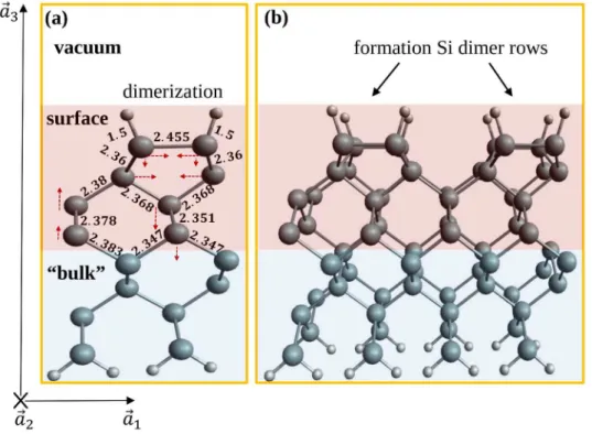
In this section we describe a finite Silicon computational box with a top reconstructed and passivated surface in which impurities, defects, dangling bonds or external potentials will be implemented. We start with a small box suitable for ab-initio calculations. Fig. 1(a) shows the computational supercell used to model a box or a slab with 8 Si layers. The top surface of Si, passivated with H atoms, aims at simulating a real Si surface and is follwed by a vacuum region in the [0,0,1] direction. The bottom surface on the other hand aims at simulating bulk silicon. This supercell is repeated periodically in the lateral and vertical directions using the lattice vectors ~a1 = a1x, ~aˆ 2 = a2yˆ and ~a3 = a3ˆz. Here a1 =
√ 2aSi,
a2 =
√
2aSi/2 and a3 = 2aSi+ hvac where aSi is the lattice constant of bulk Si and hvac is the
In order to understand the structure and electronic properties of our Si computational box we perform Density Functional Theory (DFT) calculations using the PBE generalized gradi-ent approximation to the exchange-correlation energy functional [17, 18] as implemgradi-ented in the Abinit code. [19] All calculations were performed using a plane wave basis set truncated with a kinetic energy cutoff of 20 Ha (544 eV). A grid with 6 × 12 × 1 k-points was used for Brilloin-zone integrations using Monkhorst-Pack method. [20] First, we optimized the lattice constant of bulk silicon and obtained aSi= 5.46 ˚A. Note that this value agrees up to
0.03 ˚A with the experimentally observed lattice constant of Silicon, aexpSi = 5.43. [21] Next we proceeded to surface reconstruction. First, for a given number of Si layers the thickness of vacuum above the surface was varied until total energy did not depend on it. We found that a vacuum region of 16 ˚A was enough to suppress interaction between periodic images in the ˆz direction. Next, we varied the number of Si layers of the slab and found that 8 layers
FIG. 1. (color online) (a) Optimized atomic structure of the supercell used to model top surface reconstruction of a Si-(100) slab. Bond lengths are reported explicitly in Angstrom. Dash (red) arrows indicate the displacements of Si atoms, respective to their positions in bulk material, due to surface reconstruction. (b) A larger slab supercell illustrating the formation of Si dimer rows on the slab reconstructed surface.
were sufficient to achieve convergence of the surface energy per surface unit cell. With 8 Si layers there are 16 Si atoms and 6 Hydrogen atoms in a supercell as shown in Fig. 1(a).
Surface reconstruction was achieved by minimizing total energy with respect to the atomic positions of H and Si atoms in the top four layers of the slab. Atomic coordinates were ad-justed until maximum interatomic force was less than 0.001 eV/˚A. In Fig. 1(a) we illustrate with arrows the displacements of Si atoms with respect to their positions in the bulk ma-terial. As seen in Fig. 1 the top Silicon layer is reconstructed, with formation of Si dimers passivated with H atoms. The positions of Si atoms in the bottom layers were not optimized as relaxation decreases very rapidly as we move away from the top surface. The bottom sur-face is unreconstructed and fully passivated with H atoms to simulate a seamless transition to the bulk material.
III. TIGHT-BINDING ELECTRONIC-STRUCTURE CALCULATIONS
In this section we describe the model tight binding (TB) Hamiltonian we use to approxi-mately calculate the Kohn-Sham (KS) quasi-particles of the Si slab described in the previous section. The KS quasi-particle Hamiltonian reads:
ˆ
HQP =
~p2
2m + Vatoms(~r) + VHartree(~r) + Vxc(~r), (1) where Vatoms(~r) is the sum of atomic potentials, VHartree(~r) is the Hartree potential produced
by all electrons, and Vxc(~r) is the exchange-correlation potential. If we carry out fully
self-consistent density functional calculations as in previous section, the KS Hamiltonian would have been expressed in terms of atomic, Hartree, and exchange-correlation potentials, themselves functionals of the ground state electronic density. Since we do not know the Hamiltonian for a large number of atoms, we parametrize it in a tight binding form by expanding the electron wavefunction as a linear combination of atomic orbitals (LCAO) α on atom at position ~R:
|φi =X
~ R,α
cRα~ | ~Rαi. (2)
In our tight-binding approach we retain ten valence orbitals for each Si atom: one s, three p, five d and one additional s∗ orbital that accounts for higher lying states and by one s
quantization as follows, ˆ HTB = NSi+NH X i=1 Norb(i) X α=1
εiαc+iαciα+
NSi+NH X i=1 NN(i) X j=1 Norb(i) X α=1 Norb(j) X β=1 tiα,jβc+iαcjβ. (3)
In Eq. (3) c+iα (ciα) is the creation (annihilation) operator of an electron on the orbital α
localized on the site i, εiαis the corresponding on-site energy, and tiα,jβ describes the hopping
of the particle between orbitals on neighboring sites. NSi and NHare, respectively, the total
number of Si and H atoms in the slab, Norb(i) is the number of atomic orbitals centered on site i and NN(i) is the number of nearest neighbors of the i-th atom, that is, 4 for Silicon atoms and 1 for hydrogen atoms.
Off-diagonal matrix elements (hopping parameters) of our Hamiltonian are calculated according to Slater and Koster rules.[22] In this approach the hopping parameters tiα,jβ are
expressed as geometric functions of two-center integrals and depend only on the relative positions of the two centers i and j. Contributions from three-center integrals are neglected. A detailed explanation of how to evaluate tunneling matrix elements was already published in Refs. [15,22]. Here on-site energies εα and tunneling matrix elements tiα,jβ are not directly
calculated, but obtained by fitting the TB band structure to analogous results measured experimentally or obtained by first-principles calculations. In this work, we use our own sets of TB parameters that fit the ab-initio DFT band structure of the passivated Si slab with reconstructed surface. More details about the optimized set of TB parameters are given in Sections IV and V.
IV. BAND STRUCTURE OF A Si BOX WITH HYDROGEN PASSIVATED AND
RECONSTRUCTED SURFACE - A TIGHT BINDING MODEL
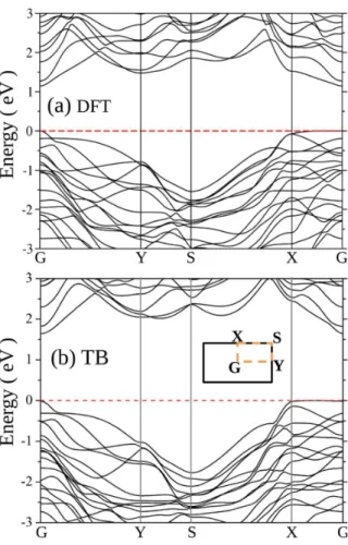
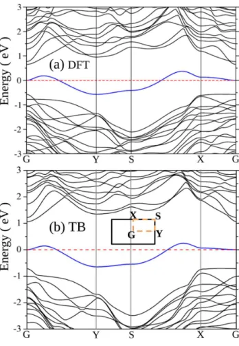
In this section we report results and comparison of tight-binding (TB) and DFT calcu-lations of the band structure of the Silicon box (slab) shown in Fig. 1. In Fig. 2(a) we plot the energy bands of the model box calculated with DFT along the path defined by the symmetry points G = (0, 0, 0), Y = (0, π/a2, 0), S = (π/a1, π/a2, 0) and X = (π/a1, 0, 0) of
the surface Brilloin zone. The supercell shown in Fig. 1(a) has 16 Si atoms and 6 H atoms. With pseudopotentials accounting for core electrons, we have a total number of Ne = 70
FIG. 2. (color online) Band structure of the reconstructed and Hydrogen passivated Silicon slab shown in Fig. 1 calculated with (a) DFT using GGA-PBE approximation and plane waves as implemented in the Abinit program and (b) a tight-binding (TB) method with a set of parameters (see Table I) optimized to reproduce the ab-initio DFT band structure. Fermi level is indicated with a dash (red) line.
level in Fig. 2 is indicated by a horizontal dash (red) line. The energy gaps at G, Y, S and X points obtained with DFT calculations are reported in Table II.
We note that the DFT band structure in Fig. 2(a) reproduces very well the results reported recently by Bohloul et al. in Ref. [23] using LDA and the projector augmented wave method implemented in Vasp. [24] We also note that DFT calculations performed within the LDA approximation by authors in Ref. [25] predict a larger electronic gap of 2.0 eV at the G point for a Si slab with a smaller lattice constant.
The lower panel of Fig. 2 shows the energy bands for the same slab obtained by di-agonalizing the tight-binding (TB) Hamiltonian in Eq. (3) assuming periodic boundary
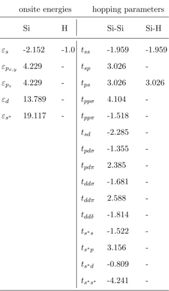
TABLE I. Parameters used in the tight-binding (TB) Hamitonian to calculate the band structure shown in Fig. 2(b). All values are in eV.
onsite energies hopping parameters
Si H Si-Si Si-H εs -2.152 -1.0 tss -1.959 -1.959 εpx,y 4.229 - tsp 3.026 -εpz 4.229 - tps 3.026 3.026 εd 13.789 - tppσ 4.104 -εs∗ 19.117 - tppπ -1.518 -tsd -2.285 -tpdσ -1.355 -tpdπ 2.385 -tddσ -1.681 -tddπ 2.588 -tddδ -1.814 -ts∗s -1.522 -ts∗p 3.156 -ts∗d -0.809 -ts∗s∗ -4.241
-conditions. Tight-binding parameters for Si atoms were taken from a parametrization by Klimeck in NEMO1D [26] that describes the experimental band structure of bulk Silicon. Then, we used a genetic algorithm to optimize the on-site energy of s-type atomic orbitals of passivating Hydrogens in order to reproduce the band structure shown in Fig. 2(a) obtained from DFT calculations. The optimized values for the s, p, d and s∗ orbital energies for Si
and H as well as required off-diagonal matrix elements are reported in Table I. As can be seen from Fig. 2(b) this set of TB parameters captures all features of the band structure predicted by DFT. Our TB parametrization predicts larger electronic gaps for all symmetry points (see Table II), this is because the TB parameters for Si atoms were fitted to the values, masses and gaps, which reproduce the experimental electronic structure of bulk Si.
TABLE II. Energy gaps between the top of the valence band and the bottom of conduction band
(Egap) plotted in Fig. 2 calculated with DFT and tight-binding (TB) methods at the points G, Y,
S and X of the surface Brilloin zone. All values are given in eV.
DFT TB
Egap(G) 1.144 1.656
Egap(Y) 2.262 3.078
Egap(S) 3.401 4.139
Egap(X) 1.592 2.496
V. DANGLING BOND WIRES ON A H:Si-(100)-(2×1) SURFACE
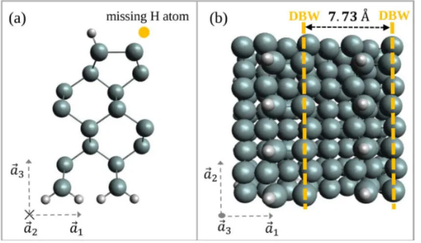
If we remove a top H atom in the supercell shown in Fig. 3(a) and apply periodic boundary conditions, the resulting slab will have an array of dangling bond wires (DBWs) along the row of Si dimers separated by a single wire of saturated bonds and H-atoms as illustrated in Fig. 3(b). This was also studied in Ref. [23] and we compare our DFT and
FIG. 3. (color online) (a) Sideview of a supercell with a missing Hydrogen atom generating an
array of infinite wires of dangling bonds (DBWs). (b) top view of a larger supercell illustrating
TB results with DFT calculations reported in Ref. [23].
In Fig. 4(a) we show results of DFT calculation of energy bands for the Si slab defined in Fig. 3. This supercell with a missing H atom has now an odd number of electrons Ne= 69,
so we performed spin-polarized DFT calculations to obtain the band structure. We did not carry out geometry optimization of the model slab. Watanabe et al. [27] performed geometry optimizations and found that the height of the unsaturated Si atoms is lowered by only 0.1 ˚A. We used a Fermi-Dirac smearing to define the occupations of spin Kohn-Sham orbitals at each k-point during self-consistent calculations. Converged results show no spin polarization, with the highest energy occupied orbital equally populated by one half of the unpaired electron. This translates into identical band structures for the two spin components.
FIG. 4. (color online) (a) Energy band (in blue) in the gap of Silicon associated with DBWs
calculated with (a) DFT and with (b) tight-binding (TB) methods. Fermi level is indicated with a dash (red) line.
In Fig. 4(b) we plot the energy bands of the same Si slab obtained by solving the tight-binding Hamiltonian, Eq. (3), with periodic boundary conditions. In our TB calculations, removal of the Hydrogen atom is accounted for by i) setting to zero hopping parameters between the unsaturated Si atom and removed H atoms, and ii) shifting the onsite energy of the s orbital centered on this H atoms well up in energy to avoid indirect coupling with other atoms. Furthermore, we adjusted onsite energies of s and p atomic orbitals of depassivated Si atoms to the values εs = −1.7 eV and εp = 2.04 eV to improve the tight-binding description
of the midgap band of DB states with respect to DFT results.
Both DFT and TB calculations show appearance of a band of states in the energy gap of Silicon, associated with the dangling bond wires. The energy band, marked in blue, describes electronic states localized on Si atoms with dangling bonds on the surface. Notice that this band shows dispersion in all directions in reciprocal space due to coupling of dangling bonds localised on different dimer rows. Furthermore, our DFT and TB calculations predict an energy-dispersion width for this band of 0.74 eV which is in excellent agreement with previous calculations. [10, 23, 27] In Table III we report the energy difference between the top of the valence band and the DB states at the symmetry points. Note that TB calculations place these states at slightly higher energies as compared with analogous results calculated using DFT.
TABLE III. Energy gaps between the top of the valence band and the midgap band of DB states
(EDB
gap) at points G, Y, S and X as plotted in Fig. 4 calculated with DFT and tight-binding (TB).
All values are given in eV.
DFT TB
EgapDB(G) 0.570 0.716
EgapDB(Y) 0.778 1.036
EgapDB(S) 1.695 1.943
VI. DANGLING BOND QUANTUM DOT ON THE SILICON SURFACE
We now turn to the description of a single dangling bond quantum dot on a passivated and reconstructed Si surface. With a single DBQD we abandon periodic boundary condi-tions in all direccondi-tions and develop a Silicon computational box (SiCB) properly passivated with Hydrogen atoms on all sides but only top reconstructed surface. Fig. 5 shows two computational boxes, labeled by the number of unit cells (n) in the directions of ~a1 and ~a2
(na1 × na2). Fig. 5(a) shows the smallest possible slab of NSi = 32 Silicon atoms
passi-vated with Hydrogen. The top layer shows reconstructed and passipassi-vated surface, the bottom surface and edges remain unreconstructed and fully saturated with H atoms with the goal of simulating a seamless transition to the bulk of Silicon. For NSi = 32 Silicon atoms this
requires NH = 40 Hydrogen atoms, with a total number of electrons Ne= 168. In Fig. 5(b),
a much larger Silicon computational slab with NSi= 256 and NH = 184, with Ne = 1208 is
shown.
These SiCBs are finite clusters and we carry out ab-initio DFT calculations using the Octopus code [28] to solve the Kohn-Sham (KS) equations in a real-space representation. The real-space simulation domain was defined by using spheres centered at the atomic positions with radius 5 ˚A and a uniform spacing of 0.19 ˚A between each grid point of the
FIG. 5. (color online) Silicon computational box (SiCB) with top reconstructed surface consisted
of (a) NSi = 32, NH = 40, Ne = 168 and (b) NSi = 256, NH = 184, Ne = 1208. The edges and
bottom surface are passivated with H atoms without reconstruction. SiCBs are labeled based on
generated mesh. We used atomic pseudopotentials to account for core electrons of Si atoms and the PBE-GGA approximation to the exchange-correlation potential. On the other hand, we performed tight-binding calculations with Si-Qnano with the parameters optimized to reproduce DFT energy bands of a Si slab as discussed in the previous sections.
Fig. 6 shows the results of DFT and tight-binding calculations for the NSi = 32 Silicon
slab. The left hand side (Fig. 6(a)) shows the energy levels of the slab fully passivated with Hydrogen. Black bars show KS orbital energies calculated with Octopus and red bars show the TB energy levels obtained with Si-Qnano. We see energy levels filled with spin up/down electrons up to the Fermi level which we take as reference energy level EF = 0.
The structure is fully passivated, there is an energy gap of Egap ≈ 3 eV opening in the
energy spectrum in both, DFT and TB, calculations. Fig. 6(b) shows the effect of a removal of a Hydrogen atom from the top surface and hence a formation of the dangling bond. The removal of a Hydrogen atom implies a removal of one electron, there are now Ne = 168 − 1
FIG. 6. (color online) (a) Energy levels of the Silicon computational box (SiCB) shown in Fig.
5(a) with top reconstructed surface passivated with Hydrogen. Q denotes the net charge of the SiCB. (b) Shows the effect of removal of a H atom from a top surface and a formation of a single dangling bond (DB) state with energy in the gap of Silicon.
electrons, with one electron on a Silicon dangling bond. In addition, we characterize the cluster by the net charge Q. Because we removed both proton and electron, the net charge remains Q = 0 even though there is a dangling bond and odd number of electrons.
The energy spectra for a surface with one dangling bond (DB) show emergence of an energy level, marked in blue, in the energy gap. As we have an odd number of electrons, in spin-polarized DFT, energy levels for spin up and spin down electrons are different, thus, we have two localized levels that appear at 0.9 eV and 1.9 eV above the top valence state, respectively. In red we show the energy spectrum for the same Silicon cluster with a DB state obtained with Si-Qnano. We see that just like in DFT calculations, there is a bound state, marked in blue, in the energy gap located at 1.5 eV above the top valence state.
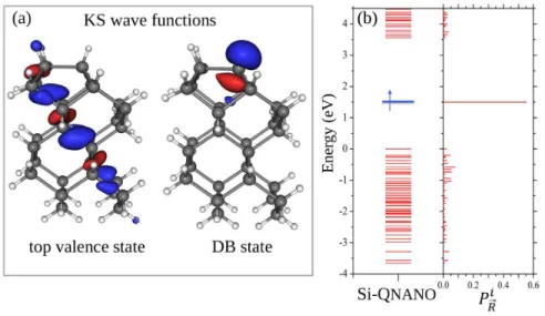
The localized nature of the dangling bond state is shown in Fig. 7. In its left panel we visualize the KS wave functions of the top valence and dangling bond states for the SiCB shown in Fig. 5(a). This figure shows that while the valence state delocalizes over several Si atoms of the cluster the wave function associated with the state in the gap is clearly localized around the Si atom with a dangling bond. Furthermore, we also notice from the plotted isosurface the pz atomic-like character of the DB KS orbital. A similar scenario is confirmed
FIG. 7. (a) Isosurfaces of Kohn-Sham (KS) wave functions of the top valence state and the
DB state with energy in the gap. (b) Energy levels of the Silicon computational box (SiCB)
1a1× 1a2 shown in Fig. 5(a) and probability density PR~i of finding the electron localized around
by tight-binding calculations. In Fig. 7(b) we plot the probability density Pi ~ R = P α|C i ~ Rα| 2,
of finding the electron localized around the Si atom with position vector ~R with a dangling bond, due to removal of a Hydrogen atom, calculated for each eigenstate |φii. We see a
distinct peak of Pi ~
R associated with the state in the energy gap indicating a strong electron
localization on the Si atom with the DB.
In Fig. 8 we show results obtained for a much larger computational box with NSi= 256
and NH = 184. We see that qualitatively the same result is obtained. The energy gap in the
spectrum appears, with the value EGap ≈ 2 eV, smaller than the energy gap for the smaller
cluster as shown in Fig. 6. Removal of a Hydrogen atom from the top surface results in the appearance of a DB state in both, DFT and TB, spectra, located at 0.4 eV and 0.9 eV, respectively, above the top valence state.
In Fig. 9 we plot the tight-binding energy spectra calculated with Si-Qnano of Si com-putational boxes of increasing size with a single dangling bond at the top surface. The
FIG. 8. (a) Energy levels of the Silicon computational box (SiCB) 4a1× 4a2 shown in Fig. 5(b),
Q denotes the net charge of the SiCB. (b) Shows the effect of removal of a H atom from a top
surface and a formation of a single dangling bond (DB) state with energy in the gap of Silicon.
(c) probability density Pi
~
R of finding the electron localized around the depassivated Si atom with
simulated slabs consist of a total number of Si atoms NSi ranging from 32 (smallest possible
cluster) to 14400, a SiCB with dimension 30a1× 30a2. We used Lanczos method, as
imple-mented in Si-Qnano to calculate the energy levels of the finite slabs close to the top of the valence band and to the bottom of conduction band. Notice that in all cases a gap opens with the appearance of a state with energy in the gap (DB state) due to the creation of a dangling bond on the top reconstructed surface. Dash (red) line in Fig. 9 shows the renor-malization of the valence and conduction band edges as the size of the systems is increased. The energy gap decreases, as expected for less confined systems and its value for the largest SiCB EGap = 1.6 eV seems to approach the TB energy gap of an infinite slab as shown in
Fig. 4. We also observe that the energy of the DB state converges very rapidly with the size of the Si slab due to the localized character of this state. For the largest SiCB with
FIG. 9. (a) Energy levels of Silicon computational boxes (SiCB) of increasing size with a single
dangling bond (DB) in the top reconstructed surface calculated with Si-Qnano. The DB state is marked in blue, the arrow indicates single-electron occupation of this state. Dash (red) lines illustrate the evolution of the top of the valence band and the bottom of conduction band with the size of the finite slab.
NSi= 14400 atoms, TB calculations with Si-Qnano place the DB state energy level 0.6 eV
above the top of the valence band.
VII. CHARGING ENERGY OF THE DANGLING BOND QUANTUM DOT
Scanning Tunneling Spectroscopy experiments show that the dangling bonds simulated in the previous section are on average neutral, that is, the DB quantum dot is occupied by a single electron. However, for n-type doped Silicon samples, additional electrons in the conduction band can be loaded into the DBQD in a controlled way using gates. [6, 8] We approximate the two-electron DBQD with a single configuration where two electrons with opposite spins are populating the DB orbital, with net charge of DBQD Q = −1. The charging energy UDB of a DBQD is given by the two-body Coulomb matrix element,
UDB = Z dx1dx2 φ∗u(x1)φ∗d(x2) e2 ǫ(x1, x2)|x1− x2| φd(x2)φu(x1), (4)
where φu and φdare spin up and spin down DB spin-orbitals, each occupied by one electron
at position x ≡ (~r) and ǫ(x1, x2) is the position-dependent dielectric function. In order to
evaluate Coulomb matrix element we express the TB orbitals in the LCAO basis, |φii = X ~ R,α Ci ~ Rα | ~Rαi|χmαi, (5)
with χ denoting the spin wave function. It follows from Eq. (5) that the Coulomb matrix element reads as,
UDB = X ~ R1,α1 X ~ R2,α2 X ~ R3,α3 X ~ R4,α4 Cu∗ ~ R1α1 C d∗ ~ R2α2 C d ~ R3α3 C u ~ R4,α4 × δmα1,mα4δmα2,mα3h ~R1α1, ~R2α2 e2 ǫ(~r1, ~r2) |~r1− ~r2| ~ R3α3, ~R4α4i. (6)
Eq. (6) contains up to four-center integrals. We restrict the terms entering the latter equation to be one-center and two-center Coulomb matrix elements. The integrals involving atomic orbitals centered on the same atom and on atoms which are nearest-neighbors (NN) are calculated numerically using Slater type orbitals to approximate the radial part of the wave functions. The two-center integrals involving atoms that are not NN are treated as long-range Coulomb interaction between two charges distributions as explained in Ref. [15].
FIG. 10. Energy of the (a) neutral and (b) charged DB state for a SiCB 4a1× 4a2 shown in Fig.
5(b) with a depassivated Si atom at the top surface calculated with DFT and Si-Qnano.
As we have shown in Fig. 7(b) and Fig. 8(c), for the dangling bond state the probability density of finding the electron localized around the depassivated Si atom peaks at the large value of 0.6. This implies that the onsite term in Eq. (6) will give most of the contribution to the charging energy UDB of the DB quantum dot. Indeed, we found that the DB charging
energy shows practically no dependence with the size of the Si computational box. On the other hand, the position-dependent dielectric function accounting for screening effects due to the valence electrons and the Si-vacuum interface has been approximated. [15] More specifically, on-site (dominant) contribution to the Coulomb interaction between the two electrons in the DB state is screened by the effective dielectric constant ǫeff = (ǫSi+ 1)/2
where εSi = 11.9 is the static dielectric constant of Silicon. [21] The smaller contributions
involving atomic orbitals centered on neighboring atoms and non-NN atoms are screened by the dielectric constants (ǫSi/2) and ǫSi, respectively.
top surface calculated with DFT and the TB approach implemented by Si-Qnano. The DB states shown in Fig. 10(a) are occupied by 1 electron which corresponds to a neutral DB quantum dot. On the other hand, Fig. 10(b) shows the energy spectra of SiCB with net charge Q = −1 where an extra electron with opposite spin populates the DB state. The DFT spectra are obtained solving the spin-unpolarized Kohn-Sham equations for the negatively charged finite Si box. Notice that in this case the KS energy of the DB state is shifted up by 1.2 eV with respect to the energy of the neutral DB state. This means that each electron occupying the DB state for the system with Q = −1 feels a KS effective potential due to the delocalized valence electrons plus a two-body Coulomb repulsion due to the presence of a second electron in the DB qdot.
A similar analysis holds for electrons occupying the TB states calculated with Si-Qnano. In this case, the energy of the DB state occupied by two non-interacting electrons will be shifted up in energy by the charging energy UDB with respect to the singly occupied DB
state. In order to compare with DFT results, we used the TB wave function of the DB state to compute the charging energy using Eq. (6) for which we obtained the value of 0.67 eV. This places the energy of the negatively charged DB state at 1.62 eV above the top of the valence band which is in excellent agreement with DFT results as shown in Fig. 10(b). In other words, our TB approach predicts a 0.67 eV upward shift for the energy level of the charged DB relative to that of the neutral DB. We note that this number is in good agreement with the value of 0.5 eV reported by Livadaru et al. in Ref. [9]. Furthermore, the charged DB energy level predicted by Si-qnano defines a bound state with energy −0.85 eV relative to the bottom of the conduction band which is similar to the value of −0.95 eV reported by authors in Ref. [11] to model STM experimental results on charged DB qdots. The small deviations of our results relative to the data reported by other authors may be related to the fact that we did not re-optimize the atomic position of the depassivated Si atom due to the excess charge localization.
VIII. CONCLUSION
We have presented Si-Qnano, a new scalable computational platform to simulate atomic scale quantum devices in silicon. We applied Si-Qnano to describe the dangling bond quantum dots on a Si-(100)-(2x1) surface passivated with hydrogen. The dangling bond was
shown to result in an energy level localised in the silicon gap, with wavefunction localised in the vicinity of the dangling bond silicon atom. The DBQD was shown to acommodate up to two electrons and charging energy was predicted. For small number of silicon atoms the Si-Qnano results agreed very well with ab-initio calculations. However, Si-Qnano allowed us to compute the electronic properties for silicon nanostructures involving tens of thousands of atoms. Future work will apply Si-Qnano to dangling bond and dopant based quantum circuits, gated quantum dots and nanocrystals in silicon.
ACKNOWLEDGMENTS
The authors thank R. Wolkow and Ken Gordon of Quantum Silicon Inc., NSERC EN-GAGE program and University of Ottawa Research Chair in Quantum Theory of Materials, Nanostructures and Devices for support.
[1] M. G. Francesco Priolo, Tom Gregorkiewicz and T. Krauss, Nature Nanotechnology 9, 19 (2014).
[2] T. Watson, S. Philips, E. Kawakami, D. Ward, P. Scarlino, M. Veldhorst, D. Savage, M. La-gally, M. Friesen, S. Coppersmith, et al., Nature 555, 633 (2018).
[3] S. Studenikin, L. Gaudreau, K. Kataoka, D. Austing, and A. Sachrajda, Applied Physics Letters 112, 233101 (2018).
[4] S. D. Sarma, R. de Sousa, X. Hu, and B. Koiller, Solid State Communications 133, 737 (2005).
[5] J. Salfi, J. Mol, R. Rahman, G. Klimeck, M. Simmons, L. Hollenberg, and S. Rogge, Nature Materials 13, 605 (2014).
[6] R. A. Wolkow, L. Livadaru, J. Pitters, M. Taucer, P. Piva, M. Salomons, M. Cloutier, and B. V. Martins, in Field-Coupled Nanocomputing (Springer, 2014) pp. 33–58.
[7] M. B. Haider, J. L. Pitters, G. A. DiLabio, L. Livadaru, J. Y. Mutus, and R. A. Wolkow, Physical Review Letters 102, 046805 (2009).
[8] M. Taucer, L. Livadaru, P. G. Piva, R. Achal, H. Labidi, J. L. Pitters, and R. A. Wolkow, Physical Review Letters 112, 256801 (2014).
[9] L. Livadaru, P. Xue, Z. Shaterzadeh-Yazdi, G. A. DiLabio, J. Mutus, J. L. Pitters, B. C. Sanders, and R. A. Wolkow, New Journal of Physics 12, 083018 (2010).
[10] P. Doumergue, L. Pizzagalli, C. Joachim, A. Altibelli, and A. Baratoff, Physical Review B 59, 15910 (1999).
[11] S. Schofield, P. Studer, C. Hirjibehedin, N. Curson, G. Aeppli, and D. Bowler, Nature Com-munications 4, 1649 (2013).
[12] R. R. Mikal Kepenekian, Roberto Robles and N. Lorente, Nanotechnology 25, 322 (2014). [13] H. Raza, Physical Review B 76, 045308 (2007).
[14] W. Sheng and P. Hawrylak, Physical Review B 72, 035326 (2005).
[15] M. Zieli´nski, M. Korkusi´nski, and P. Hawrylak, Physical Review B 81, 085301 (2010).
[16] M. Korkusinski, O. Voznyy, and P. Hawrylak, Physical Review B 84, 155327 (2011). [17] J. P. Perdew, K. Burke, and M. Ernzerhof, Physical Review Letters 77, 3865 (1996). [18] J. P. Perdew, K. Burke, and M. Ernzerhof, Physical Review Letters 78, 1396 (1997).
[19] X. Gonze, B. Amadon, P.-M. Anglade, J.-M. Beuken, F. Bottin, P. Boulanger, F. Bruneval, D. Caliste, R. Caracas, M. Ct, T. Deutsch, L. Genovese, P. Ghosez, M. Giantomassi, S. Goedecker, D. Hamann, P. Hermet, F. Jollet, G. Jomard, S. Leroux, M. Mancini, S. Mazevet, M. Oliveira, G. Onida, Y. Pouillon, T. Rangel, G.-M. Rignanese, D. Sangalli, R. Shaltaf, M. Torrent, M. Verstraete, G. Zerah, and J. Zwanziger, Computer Physics Com-munications 180, 2582 (2009).
[20] H. J. Monkhorst and J. D. Pack, Physical Review B 13, 5188 (1976).
[21] O. Madelung, Semiconductors: data handbook (Springer Science & Business Media, 2012). [22] G. F. Koster and J. Slater, Physical Review 95, 1167 (1954).
[23] S. Bohloul, Q. Shi, R. A. Wolkow, and H. Guo, Nano Letters 17, 322 (2016).
[24] G. Kresse and J. Furthm¨uller, Physical Review B 54, 11169 (1996).
[25] N.-P. Wang, M. Rohlfing, P. Kr¨uger, and J. Pollmann, Physical Review B 74, 155405 (2006).
[26] T. B. Boykin, G. Klimeck, and F. Oyafuso, Physical Review B 69, 115201 (2004).
[27] S. Watanabe, Y. A. Ono, T. Hashizume, and Y. Wada, Physical Review B 54, R17308 (1996). [28] X. Andrade, D. Strubbe, U. De Giovannini, A. H. Larsen, M. J. Oliveira, J. Alberdi-Rodriguez, A. Varas, I. Theophilou, N. Helbig, M. J. Verstraete, et al., Physical Chemistry Chemical Physics 17, 31371 (2015).