HAL Id: cea-01973699
https://hal-cea.archives-ouvertes.fr/cea-01973699
Submitted on 8 Jan 2019
HAL is a multi-disciplinary open access
archive for the deposit and dissemination of
sci-entific research documents, whether they are
pub-lished or not. The documents may come from
teaching and research institutions in France or
abroad, or from public or private research centers.
L’archive ouverte pluridisciplinaire HAL, est
destinée au dépôt et à la diffusion de documents
scientifiques de niveau recherche, publiés ou non,
émanant des établissements d’enseignement et de
recherche français ou étrangers, des laboratoires
publics ou privés.
Size-dependent carrier mobilities in rectangular silicon
nanowire devices
Zaiping Zeng, Francois Triozon, Yann-Michel Niquet, Sylvain Barraud
To cite this version:
Zaiping Zeng, Francois Triozon, Yann-Michel Niquet, Sylvain Barraud. Size-dependent carrier
mobili-ties in rectangular silicon nanowire devices. 2016 International Conference on Simulation of
Semi-conductor Processes and Devices (SISPAD 2016), Sep 2016, Nuremberg, Germany.
pp.257-260,
Size-dependent carrier mobilities in rectangular
silicon nanowire devices
Zaiping Zeng
1,2, Yann-Michel Niquet
1,2,∗, Franc¸ois Triozon
3,2, and Sylvain Barraud
3,21CEA, INAC-MEM, L Sim, Grenoble, France 2 University Grenoble Alpes 3CEA, LETI-MINATEC, Grenoble, France
∗e-mail: [email protected]
Abstract— Multi-gate transistors have attracted consid-erable attention as a way to overcome the scaling issues of planar MOSFETs. Although the effects of structural confinement on the carrier mobilities have been discussed extensively, the transition from silicon thin films to silicon nanowires (SiNWs) has been little investigated. In this contribution, we perform quantum calculations of the size-dependent carrier mobilities in gate-all-around rectangular SiNWs with leading dimension up to 50 nm, in the non-equilibrium Green’s functions (NEGF) framework. We find that when the smallest width or height falls in the sub-10 nm range, nearest neighbor corner channels tend to merge and form “side channels” with much lower mobilities. On top of the numerical results, we have derived a simple model, which bridges square NW devices with thin film devices, and describes the size dependence of the carrier mobilities in rectangular SiNWs in a wide range of dimensions.
I. INTRODUCTION
In a continuous effort to increase drive current and to control short-channel effects, Metal-Oxide-Semiconductor (MOS) transistors have evolved from classical, planar, single-gate devices to three-dimensional devices with a multi-gate structure [Double-Gate (DG), Tri-gate or Gate-All-Around (GAA) devices] [1]. Among multi-gate architectures, GAA silicon nanowire (SiNW) transistors demonstrate the best gate control and hence the best short-channel figures (sub-threshold slopes, drain-induced barrier lowering, ...). Consequently, con-siderable attention has been devoted to the study of GAA devices [2]–[7]. Although significant insights have been brought by these studies, the transition from silicon thin films to SiNWs has been little investigated up to now. In this work, we discuss how the carrier mobilities vary when going from SiNWs to silicon thin films.
In order to achieve a consistent description of this transition, we have performed quantum calculations in the Non-Equilibrium Green’s Functions (NEGF) frame-work on rectangular SiNWs with leading dimension up to 50 nm. Based on the numerical results, we have developed a simple model, which bridges the DG devices with the square GAA (SQGAA) NW devices, and which describes the size dependence of the carrier mobilities in rectangular SiNWs over a wide range of dimensions.
II. METHODOLOGY AND DEVICES The simulated devices are rectangular GAA SiNW channels with width W and height H. Both the h100i [with {001} facets] and h110i [with horizontal (001) and vertical (1¯10) facets] nanowire orientations are consid-ered. The gate-stack is made of 0.6 nm of SiO2 and 2.4
nm of HfO2. The transport properties of the SiNWs are
computed in a NEGF framework based on the effective mass approximation for the electrons and on a three bands k · p model for the holes. The NEGF equations are solved self-consistently in a fully coupled mode space approach [8]. In our calculations, we have taken into account the carrier-phonon and surface roughness (SR) scatterings. The local approximation has been adopted for the carrier-phonon self-energy. The SR profiles are generated from a standard Gaussian autocorrelation func-tion model with rms fluctuafunc-tions ∆ = 0.45 nm and correlation length Lc= 1.0 nm. A detailed review of the
methodology and the parameters for the carrier-phonon interactions can be found in Refs. [9] and [10]. The carrier mobilities are computed from a quasi-Fermi level analysis [11] on a 30 nm-long channel.
III. RESULTS AND DISCUSSION
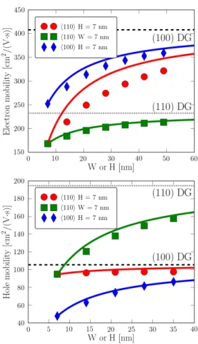
We first discuss the electron and hole mobilities in rectangular SiNWs as a function of the width W and height H. The NEGF mobilities are computed in rect-angular SiNWs with one side (H or W ) equal to 7 nm and the other one ranging from 7 to 50 nm for electrons and from 7 to 35 nm for holes. The results are plotted in Fig. 1 (symbols). Note that H and W play equivalent roles in [100] SiNWs (which have equivalent (010) and (001) facets, but not in [110] SiNWs (which have non-equivalent (001) and (1¯10) facets).
For electrons, we find that (i) h100i SiNWs perform better than h110i SiNWs, and (ii) h110i SiNWs with width W > H show larger mobilities than h110i SiNWs with height H > W . These trends can be well understood from band structure arguments [12].
In [100] SiNWs, the ∆ valleys split into light (m∗ = 0.19 m0) ∆y,z valleys at the Γ point, and much heavier
(m∗ = 0.92 m0) ∆x valleys at k 6= 0. Under strong
inversion bias, the electron gas is confined at the surface of the SiNW by the electric field, mostly in the light ∆y
Fig. 1. Electron (upper panel) and hole (lower panel) mobilities in rectangular h100i and h110i GAA SiNWs as a function of width (W ) or height (H) at carrier density n = 8 × 1012cm−2. The symbols are
the NEGF results. The dashed and dotted horizontal lines are the NEGF reference mobilities in (100) and (110) DG devices, respectively. The solid lines are the interpolations from SQGAA NW devices to the limiting DG devices using Eq. (2).
valleys on the lateral (010) facets, and mostly in the light ∆z valleys on the top and bottom (001) facets. In [110]
SiNWs, the ∆ valleys split into light (m∗ = 0.19 m0)
∆z valleys at Γ point and heavier (m∗ = 0.55 m0)
∆x,y valley off Γ. Again, under strong inversion bias the
electron gas is mostly confined in the light ∆zvalleys on
the top and bottom (001) facets, but in the heavier ∆x,y
valleys on the lateral (1¯10) facets. Therefore, wide h110i SiNWs with dominant (001) facets (W > H) perform better than tall h110i SiNWs with dominant (1¯10) facets (H > W ). Likewise, h001i nanowires with only (001) facets show better mobilities than h110i SiNWs with mixed facets.
The trends are opposite for holes. h110i SiNWs with H > W indeed perform better than h110i SiNWs with W > H, and h110i SiNWs always outperform h100i
Fig. 2. Contour plot of the charge density distribution in a rectangular h100i-oriented GAA SiNW device with (W , H) = (7 nm, 49 nm).
Fig. 3. Schematic representation of the partition of the charge distribution of Fig. 2 into two contributions, one from the side channels (outer region) with thickness T , and one from the inner region with thickness H − 2T .
SiNWs. Again, these trends can be explained by band structure arguments. Indeed, holes confined on {110} facets tend to show lighter transport masses than holes confined on {001} facets [13]; in square h110i SiNWs the highest valence subband has a clear light hole char-acter and is well separated from the others, while in in square h100i SiNWs the topmost valence bands are almost degenerate and heavy, which decreases carrier velocity and enhances inter-subband scattering [12].
In general, the mobility increases with increasing SiNW cross section, and tends to the expected DG limit (W or H −→ ∞). However, the convergence can be rather slow, especially for electrons in h110i SiNWs with W > H. In order to understand the physics behind, we have analyzed the carrier density in the devices (Fig. 2). For simplicity – but without loss of generality – we focus on electrons. As shown in Fig. 2, the density in the moderate to strong inversion regime peaks in four “corner channels” that tend to merge in two “side channels” when H or W is in the sub-10 nm range. The electron (e) or hole (h) mobility can then be written:
µ(e,h)= n
(e,h) in
n(e,h)in + n(e,h)out
µ(e,h)DG + n
(e,h) out
n(e,h)in + n(e,h)out µ(e,h)out ,
(1) where nin and nout are the charge densities per unit
length in the inner and outer (side channels) regions of Fig. 3, and µDGis the mobility in the limiting DG device.
Fig. 4. Upper panel: Mobility computed in 7 nm-thick (100) and (110) DG devices, and mobility µout in the side channels extracted
from the data for the h110i SiNWs with W = 7 nm or H = 7 nm (T = 3.5 nm). Lower panel: Mobility in a h110i SiNW with (W , H) = (7 nm, 35 nm), as computed with NEGF and as obtained from Eq. (1) using the extracted mobility in the side channels.
The mobility µout in the side channels can be extracted
from the data at a given size [e.g., W = 7 nm and H = 14 nm when H > W ]. The extracted µoutis shown
in Fig. 4 for h110i SiNWs. Eq. (1) turns out to give an excellent description of the mobility at all sizes and densities (see the lower panel of Fig. 4 for example). µout
depends on the carrier density and facet orientation. It is, as expected, lower on (1¯10) than on (001) facets, and lower than in the corresponding DG device due to lateral quantum confinement in the side channel and enhanced surface roughness and phonon scattering.
The charge density nin in the inner region increases
linearly with W or H, while the charge density nout in
the side channels is almost independent on the leading dimension (see Fig. 5). Actually, charge accumulation in both inner and outer regions is ruled by simple electrostatics, e.g. nin ' α(W − 2T ) and nout '
Fig. 5. Charge density in the inner region (nin) and in the outer region
(nout) as a function of the height H in h100i Si NWs. Here, W = 7
nm, T = 3.5 nm, and the total charge density is n = 1.2 × 1013 cm−2.
α(H + 2T ) when W > H. Then Eq. (1) turns into a simple interpolation formula between the mobility µSQ
of the square NW (H = W ) and the mobility µDG of
the limiting double gate device, namely:
µ(e,h)≈W − H W + Hµ (e,h) DG + 2H W + Hµ (e,h) SQ (2) when W > H, and: µ(e,h)≈H − W W + Hµ (e,h) DG + 2W W + Hµ (e,h) SQ (3)
when W < H. These equations reproduce the NEGF data very well in most cases, as shown in Fig. 1. Therefore, this model, which only requires the square GAA and DG mobilities as input, is able to describe the size dependence of the carrier mobilities in rectangular SiNWs over a wide range of dimensions and carrier densities.
CONCLUSIONS
In a real space NEGF framework, we have performed quantum calculations on the size-dependent carrier mo-bilities in gate-all-around rectangular silicon nanowire devices. We find that the carrier mobilities improve when increasing the leading dimension and converge to the expected double gate limit. However, when the smallest dimension falls in sub-10 nm range, the four corner channels merge into two side channels with low mobility. Their contribution remains significant even in rectangular devices with large width or height up to 50 nm, so that the mobility may be slow to converge to the double gate limit in some cases. On top of the numerical results, we have derived a simple model for the size-dependent carrier mobilities, which bridges the square gate-all-around nanowire devices with the thin film devices. This model may be used in the compact modeling of gate-all-around transistors.
ACKNOWLEDGEMENTS
This work was supported by the French National Research Agency (ANR) project NOODLES, and partly supported by the IBM program and the European Unions Horizon 2020 research and innovation program under grant agreement No. 688101 SUPERAID7. The calcu-lations were run on the TGCC/Curie machine thanks to allocations from GENCI and PRACE.
REFERENCES
[1] J.-P. Colinge, FinFETs and Other Multi-Gate Transistors. Springer US, 2008.
[2] Y.-M. Niquet, C. Delerue, and C. Krzeminski, “Effects of strain on the carrier mobility in silicon nanowires,” Nano Letters, vol. 12, no. 7, pp. 3545–3550, 2012.
[3] I. Tienda-Luna, J. Roldn, F. Ruiz, C. Blanque, and F. Gamiz, “An analytical mobility model for square gate-all-around mosfets,” Solid-State Electronics, vol. 90, pp. 18 – 22, 2013.
[4] R. Rhyner and M. Luisier, “Atomistic modeling of coupled electron-phonon transport in nanowire transistors,” Phys. Rev. B, vol. 89, p. 235311, Jun 2014.
[5] R. Granzner, V. M. Polyakov, C. Schippel, and F. Schwierz, “Empirical model for the effective electron mobility in silicon nanowires,” IEEE Transactions on Electron Devices, vol. 61, no. 11, pp. 3601–3607, 2014.
[6] J. W. Ma, W. J. Lee, J. M. Bae, K. S. Jeong, S. H. Oh, J. H. Kim, S.-H. Kim, J.-H. Seo, J.-P. Ahn, H. Kim, and M.-H. Cho, “Carrier mobility enhancement of tensile strained si and sige nanowires via surface defect engineering,” Nano Letters, vol. 15, no. 11, pp. 7204–7210, 2015.
[7] H. Ryu, “A multi-subband monte carlo study on dominance of scattering mechanisms over carrier transport in sub-10-nm si nanowire fets,” Nanoscale Research Letters, vol. 11, no. 1, pp. 1–9, 2016.
[8] J. Wang, E. Polizzi, and M. Lundstrom, “A three-dimensional quantum simulation of silicon nanowire transistors with the effective-mass approximation,” J. Appl. Phys., vol. 96, no. 4, pp. 2192–2203, 2004.
[9] Y.-M. Niquet, V.-H. Nguyen, F. Triozon, I. Duchemin, O. Nier, and D. Rideau, “Quantum calculations of the carrier mobility: Methodology, matthiessen’s rule, and comparison with semi-classical approaches,” J. Appl. Phys., vol. 115, no. 5, p. 054512, 2014.
[10] V. Nguyen, Y. Niquet, F. Triozon, I. Duchemin, O. Nier, and D. Rideau, “Quantum modeling of the carrier mobility in fdsoi devices,” IEEE Transactions on Electron Devices, vol. 61, no. 9, pp. 3096–3102, 2014.
[11] L. Bourdet, J. Li, J. Pelloux-Prayer, F. Triozon, M. Casse, S. Barraud, S. Martinie, D. Rideau, and Y.-M. Niquet, “Contact resistances in trigate and finfet devices in a non-equilibrium green’s functions approach,” J. Appl. Phys., vol. 119, no. 8, p. 084503, 2016.
[12] Y. M. Niquet, C. Delerue, and D. Rideau, “Orientational and strain dependence of the mobility in silicon nanowires,” in 2012 13th International Conference on Ultimate Integration on Silicon (ULIS), 2012, pp. 49–52.
[13] P. Packan, S. Cea, H. Deshpande, T. Ghani, M. Giles, O. Golonzka, M. Hattendorf, R. Kotlyar, K. Kuhn, A. Murthy, P. Ranade, L. Shifren, C. Weber, and K. Zawadzki, “High per-formance hi-k + metal gate strain enhanced transistors on (110) silicon,” in 2008 IEEE International Electron Devices Meeting, 2008, pp. 1–4.