HAL Id: hal-01234236
https://hal.archives-ouvertes.fr/hal-01234236
Submitted on 26 Nov 2015
HAL is a multi-disciplinary open access archive for the deposit and dissemination of sci-entific research documents, whether they are pub-lished or not. The documents may come from teaching and research institutions in France or abroad, or from public or private research centers.
L’archive ouverte pluridisciplinaire HAL, est destinée au dépôt et à la diffusion de documents scientifiques de niveau recherche, publiés ou non, émanant des établissements d’enseignement et de recherche français ou étrangers, des laboratoires publics ou privés.
A generic Reverse Conducting IGBT structure for
monolithic switching cells integration
Adem Lale, Abdelhakim Bourennane, Abdelilah El Khadiry, Frederic
Richardeau
To cite this version:
Adem Lale, Abdelhakim Bourennane, Abdelilah El Khadiry, Frederic Richardeau. A generic Reverse Conducting IGBT structure for monolithic switching cells integration. Power Electronics and Ap-plications (EPE’14-ECCE Europe), 2014 16th European Conference on., Aug 2014, Lappeenranta, Finland. �10.1109/EPE.2014.6910977�. �hal-01234236�
A generic Reverse Conducting IGBT structure for monolithic switching
cells integration
Adem LALE
1,3, Abdelhakim BOURENNANE
1,3, Abdelilah EL KHADIRY
1,2, Frederic
RICHARDEAU
4,51
CNRS, LAAS, 7 avenue du Colonel Roche, F-31400 Toulouse, France
2Univ de Toulouse, LAAS, F-31400 Toulouse, France
3
Univ de Toulouse, UPS, LAAS, F-31400 Toulouse, France
4Université de Toulouse; INP, UPS; LAPLACE
(Laboratoire Plasma et Conversion d'Energie)
ENSEEIHT, 2 rue Charles Camichel, BP 7122, F-31071 Toulouse cedex 7, France
5
CNRS; LAPLACE; F-31071 Toulouse, France
Acknowledgements
«This research work received financial support from the National Research Agency (ANR). The project name is "ConvPlUS", ANR-13-JS09-0008-01»
Keywords
«Monolithic power integration», «IGBT», «Thyristor», «Converter circuit», «Device simulation»
Abstract
A generic structure of a Reverse Conducting IGBT (RC-IGBT) that integrates monolithically an IGBT for the forward conduction and a self-firing thyristor for the reverse conduction is proposed. As compared to the conventional RC-IGBT, the structure that we propose doesn’t exhibit snap-back in the forward conducting mode [1], [2]. The static and dynamic performances of the structure are investigated in this paper by 2D SentaurusTM numerical simulations. The proposed structure is then
used to design two complementary monolithic power chips, named “Common Anode three-pole” and “Common Cathode three-pole”, within the context of “two-chip” integration of static power converter [4]. These two chips are then associated to form a complete inverter. The proposed three-pole common cathode chip uses a P+ wall for insulation between the two adjacent RC-IGBT sections. The proposed
elementary RC-IGBT uses also the P+ wall in order to ensure the thyristor triggering in the reverse
conducting mode.
Introduction
The use of an anti-parallel diode with a unidirectional conventional IGBT is required in inverter and reversible chopper applications. This allows the converter to have reversibility in current and, by extension, operate in four quadrants for AC/DC and AC/AC applications. In general, the anti-parallel diode is externally co-packed with the IGBT. This leads to increased cost for the separate devices and testing time and makes the circuit bulky. Moreover, the wire bonds are source of reliability problems and source of parasitic inductance that consequently require to slow-down the IGBT switching.
The RC-IGBT is a device that integrates monolithically an IGBT and a diode [1], [2], [5], [6], [10-22]. At the device level, the RC-IGBT allows, compared to the discrete association of IGBT and diode, to reduce the silicon chip. At the power module level, the integration of IGBT and diode permits to reduce the number of chips, to simplify the interconnection and consequently to improve the reliability of converter. This approach allows on one hand, at same package; to process more power; and on the other hand, at same processed power, to reduce the active area of the chip soldered on the DBC/SMI substrate and consequently the cost.
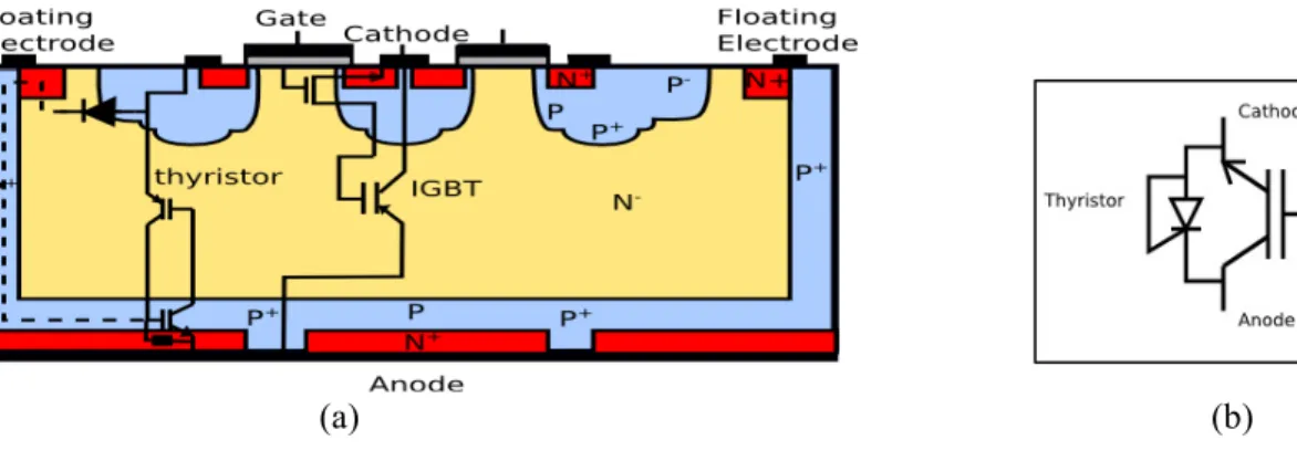
The domain of power hybrid integration aims at producing a power electronics which is more compact and more reliable. It is in this context that the monolithic multi-switch integration approach based on the monolithic integration of several RC-IGBT has been reported [4], [7-9]. The approach consists in integrating the IGBTs sharing the common anode electrode in the same Si-chip, and the RC-IGBTs sharing the common cathode electrode in another Si-chip [8]. These two complementary power chips named respectively “three-pole common anode” and “three-pole common cathode” are represented in figure 1. They can be associated to realize converters dedicated to low and medium power applications. The common cathode chip requires insulation between the RC-IGBT sections. For that purpose, a P+ wall is used in this study.
The conventional RC-IGBT has a drawback in the forward conducting mode. Indeed, it exhibits an undesirable snapback due to the change from a VDMOS to an IGBT mode in the forward conducting mode [2].
In this paper, we propose an RC-IGBT structure that integrates monolithically an IGBT and a self-firing thyristor for the reverse conduction. The architecture of this RC-IGBT doesn’t exhibit a snapback phenomenon in the forward conducting mode.
(a)
(b) (c)
Fig. 1: (a) Multi-switch two-chip based integration approach; Cross-sectional view of two three-poles structures that use conventional RC-IGBT: (b) Common anode three-pole chip, (c) Common cathode three-pole chip [3], [4].
Structures and operating modes of the proposed RC-IGBT and three-pole
devices
RC-IGBT structure
The cross sectional view of the proposed RC-IGBT structure is given in figure 2. This latter is based on the integration of an IGBT and a self-firing thyristor. The integration of the thyristor was achieved by inserting N+ diffusion in the backside P region of the classical IGBT. The thyristor is formed by the succession of four regions Pcathode/N-substrat/Panode/N+anode. A P+ wall extending from the topside to the
back-side of the silicon wafer allows the thyristor turn-on. The first thyristor cells that are near to the P+ walls are named pilot self-firing thyristor sections. Once the pilot self-firing thyristor section turns-on, the turn-on expands to the remaining part of the chip.
In the reverse conducting mode of the RC-IGBT, anode current flows from the cathode electrode to the anode electrode through the Pcathode/N-substrat junction, floating electrode, P+ wall then the P/P+anode
PN+ N+P P+ P+ Grille2 Cathode Anode1 N+ P+ P$ P$ PN+ N+P P+ P+ Grille1 N+ P+ P$ P$ RC1IGBT1 RC1IGBT2 P$ P$ P$ P$ Anode2 P+ Anode2 Anode1 Cathode N" PN+ N+P P+ P+ Grille2 Cathode2 Anode N+ P+ P" P" PN+ N+P P+ P+ Grille1 Cathode1 N+ P+ P" P" RC1IGBT1 RC1IGBT2 Cathode1 Cathode2 Anode R"drift Short+anode Short+anode 300µm 1,25"mm 0,54mm 5,6mm 2mm Anode" P+ N+ N+ P+ P+ P+ n"cellules P+ P N+ P+"("JTE) Oxyde N+ Oxyde IGBT"1"("grille"1,"cathode"1") IGBT"2"("grille"2,"cathode"2") Short&anode P+ N+ N+ P+ .P +
P& P& P&
IGBT.1.(.grille.1,.cathode.) IGBT.2.(.grille.2,.cathode.) Anode.1 Anode.2 P& P& P& Oxyde P N+ P&.(.JTE) Oxyde P+ N& M ur .d ’is o la ti o n. P+ 300µm 0,54mm 1,25mm 5,6mm 2mm n.cellules Short&anode N&
region. The pilot thyristor turn-on occurs when the voltage across the backside Panode/N+anode junction
reaches 0.7 V.
(a) (b)
Fig. 2: (a) Cross sectional view of the proposed RC-IGBT structure, (b) Symbol
Multi-pole monolithic complementary chips: Common Anode and Common Cathode
chips
The RC-IGBT structure is used to design common anode and common cathode three-pole power chips. The adopted integration approach follows the same integration strategy proposed and validated by 2D simulations in [3], [4].
The three main electrodes of the common anode chip are shown in figure 3a: two cathode electrodes, between which a 600 V voltage is applied, and an anode electrode which is common to the two integrated RC-IGBTs. The P+ walls necessary to trigger the thyristors in the reverse conducting mode
of the RC-IGBT are placed at the periphery of the three-pole common anode chip.
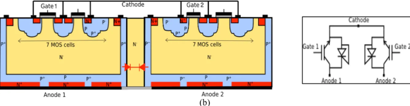
The common cathode three-pole represented in figure 3b has also three electrodes: two anode electrodes, between which a 600 V voltage is applied, and a cathode electrode which is common to two RC-IGBTs. Unlike the common anode structure, the common cathode structure requires insulation between the RC-IGBT sections. Indeed, without this insulation region, the application of a voltage between the anode electrodes results in a lateral current across the N- drift region of the three-pole common cathode structure. We make use of the P+ walls present in the proposed RC-IGBT for that
purpose in the common cathode three-pole chip. This creates two anti-series connected P+N- junctions
as represented in figure 3b. The technological realization of the P+ walls relies on a RIE of deep
trenches in the silicon wafer, then the trenches are filled with highly boron doped polysilicon, acting as a P-type doping source. After a diffusion step, the boron impurities diffuse into silicon so that the overlap of boron diffusion creates the P+ vertical wall.
(a)
(b)
Fig. 3: Cross-sectional view of the simulated three-pole structures and their schematic representation: (a) Common anode chip, (b) Common cathode chip.
Simulations results
The simulated structure has a thickness of 110 !m and a doping of 1014 cm-3. The ambient temperature
is set at 300 K. The active surface of the RC-IGBT chip only is of 1 cm2, and it is 2 cm2 for the three-pole chips. All 2D numerical simulations are carried-out under SentaurusTM TCAD simulation tool.
RC-IGBT structure operating modes
A half structure composed of 7 MOS cells and a junction termination extension (JTE) P- of 70 !m
wide (Fig. 4a) is simulated. The vertical P+ wall has a width of 10 !m. The technological parameters of the structure used during simulations are listed in table 1.
The I(V) characteristic of the simulated RC-IGBT structure is given in figure 4b. One can easily notice that there is no snapback in the forward conducting mode. In the reverse conducting mode, one can notice a snapback due to the thyristor turn-on. This turn-on takes place at low anode current density and at a voltage of about 1.4 V. It should be noted that the turn-on current and voltage of the pilot self-firing thyristor depends mainly on the physical and geometrical parameters of the Panode region above
the backside N+anode region.
Table I. Physical and geometrical parameters of the simulated RC-IGBT structure
Region Dimension (!") Surface concentration (cm-3)
SiO2 LG = 30 --- N+ L N+= 5 XN+ = 1 10+20 P Lp= 22 Xp = 5 2,5×10+17 P+ L p+ = 8 Xp+ = 7 5×10+19 channel Lch = 3 --- P+ wall LM = 10 5×10+19 JTE LT = 70 X = 4,5 9×10 +15 Panode L = 540 X = 5 5×10 +16 P+ anode L = 30 X = 7 5×10+18 N+ anode L = 265 X = 1 10+20
(b) (c)
(d) (e)
Fig. 4: (a) Cross section of the simulated RC-IGBT, (b) IA(VAK) characteristics of the proposed
RC-IGBT, (c) Distribution of the forward current density (IGBT) at Ianode=100 A, (d) Thyristor turn-on, (e)
Distribution of the reverse current density (thyristor) at Ianode=-100 A.
Thyristor switching characteristics
The study of the thyristor switching has been carried-out by simulating the RC-IGBT structure in a chopper circuit as shown in figure 5a. The control signals are given in figures 5b.
Figure 5c shows the current and voltage waveforms across the thyristor within one switching cycle. The reverse recovery and forward recovery phenomena are observed at the turn-off (t=5ms) and the turn-on (t=6ms) of the RC-IGBT, respectively. The applied gate control voltage is a PWL pulse with rise time = 2 !s and peak voltage = 15 V. The results are shown in figure 5d and 5e.
At the thyristor turn-off, the current decreases with a slope di/dt of 980 A/!s. It should be noted that the value of this latter depends both on the gate control signal and on the circuit. This current becomes
negative and reaches a peak value of -317 A and then decreases to zero. For the simulated structure, the reverse recovery time is about 1 !s (Fig. 5d).
In turn-on we observe a voltage overshoot across the device with a peak value of 42 V and a current that increases with a slope of 0,014 A/!s.
(a) (b)
(c) (d)
(e)
Fig. 5: (a) Simulated electrical circuit, (b) Gate control signal, (c) Current and voltage waveforms across the thyristor within one switching cycle, (d) Zoom on the turn-off phase of the thyristor, (e) Zoom on the turn-on phase of the thyristor.
2D simulations of the three-pole structures
The monolithic integration of the proposed RC-IGBT structure permitted to design two complementary multi-pole chips: common anode/backside and common cathode/front side. We validated by simulations the integration approach on two complementary three-poles chips. For the simulations, each three-pole chip is composed of two IGBT structures. Moreover, when one RC-IGBT section is in on state, the other RC-RC-IGBT is in OFF-state and must support the applied voltage (600 V in this case). Therefore, the electrical interactions between the RC-IGBT must be limited to an acceptable level.
To validate by 2D simulations the current bidirectionality of the proposed structures and analyse the impact of the current conduction of one RC-IGBT section on the adjacent RC-IGBT section which is
in OFF-state and supports the applied voltage, we have simulated two three-pole structures in identical conditions: one section is in ON-state while the other is in OFF-state, a voltage is applied between electrodes (anodes or cathodes depending on the type of simulated three-pole structure) and a bidirectional DC-current source injects a current of 100 A from the common electrode.
Common Anode Chip
A 600 V DC-voltage is applied between the cathode electrodes. The right RC-IGBT section is in ON-state with a gate bias of 15 V while the left section is in OFF-ON-state with the gate-to-cathode voltage being set at 0 V. A bidirectional DC-current is connected to the common anode electrode.
Figure 6a shows the equipotential lines in the RC-IGBT section which is in OFF-state. Figures 6b and 6c show the current density distribution in the RC-IGBT section which is in ON-state for both the forward (IGBT) and the reverse (thyristor) conducting modes.
(a) (b)
(c)
Fig. 6: (a) Equipotential lines distribution, (b) Current density distribution in IGBT mode, (c) Current density distribution in thyristor mode (reverse conducting mode)
Common Cathode chip
Similar simulations were carried-out for the case of the three-pole common cathode chip. A 600 V DC-voltage is applied between the anode electrodes. The right RC-IGBT section is in ON-state with the gate-to-cathode voltage being set at 15 V. The left RC-IGBT section is however in OFF-state with the gate-to-cathode voltage being set at 0 V. A bidirectional DC-current is connected to the common cathode electrode.
Figure 7a shows the equipotential lines distribution in the RC-IGBT section which is in OFF-state. We can notice that the junction P+wall/N-substrate is reverse biased and supports the applied voltage. The
depletion region expands mainly in the N- region. Figures 7b and 7c show the current densities in the
RC-IGBT section which is in ON-state section for the two operating modes: forward (IGBT mode) and reverse (thyristor mode).
(a) (b)
(c)
Fig. 7: (a) Equipotential lines distribution, (b) Current density distribution in IGBT mode, (c) Current density distribution in the thyristor mode
2D Simulation of the two three-poles complementary chips in an inverter application
The previous common anode and common cathode chips were associated to form an inverter (Fig. 8a). The inverter circuit shown in figure 8a was then simulated using SentaurusTM mixed mode simulation.
The results are shown in figures 8b and 8c. A 100 A DC-current source is inserted between the switching cells. A 600 V DC-voltage source is applied between the anode electrode of the common anode chip and the cathode electrode of the common cathode chip. The IGBTs are controlled and a dead time of 1 !s was used. The applied gate control voltage is a PWL pulse with rise time = 2 !s and peak voltage = 15 V.
(b) (c)
Fig. 8: (a) Simulated inverter circuit resulting from the association of the two complementary three-poles; Output characteristics for the case of: (b) Bipolar control type, (c) Unipolar control type
Experimental results
The experimental validation of the operating modes of proposed architectures requires the realization of the vertical P+ wall as described previously. The development of this specific technological step is
in progress at the micro and nanotechnologies platform in the Laboratory of Analysis and Architecture of Systems. It should be noted that the operating modes of the common anode chip (Fig. 1b) were recently validated by the authors [4], [8], [17]. The realized common anode chip integrates two classical RC-IGBT structures. Each classical RC-IGBT is composed of an IGBT and a PiN diode, i.e. it does not use a vertical P+ wall. The realized devices [23] are given in figure 9a and the electrical
characterization results of the RC-IGBT in the forward and reverse conducting modes are given in figures 9b and 9c.
(a) (b)
(c)
Fig. 9: (a) Realized common anode chip [23], (b) RC-IGBT forward I(V) characteristics (IGBT mode), (c) RC-IGBT reverse conduction (PiN diode conduction)
Conclusion
An RC-IGBT structure based on the monolithic integration of an IGBT and a self-firing thyristor is presented and its operating modes were validated through 2D physical SentaurusTM simulations. This
Cathode1 Cathode2 Gate2
Gate1
Gate Cathode
Common anode chip
RC-IGBT chip
a)
b)
Fig. 10. Devices realization and characterization a) wafer top view, b) on-wafer electrical characterization
Fig. 11 and Fig. 12 show the forward and reverse on-state I(V) characteristics of the realized RC-IGBTs, respectively. The channel conduction of the RC-IGBT in the reverse mode is shown in Fig. 13 this propriety of this device permits the reduction of the thermal losses in switching modes. Fig. 14 shows the I(V) characteristics of the two RC-IGBT sections that compose the common anode chip for the case in which one RC-IGBT section is in on-state while the other RC-IGBT section is in off-state. It can be easily seen that the leakage current level through the RC-IGBT section in off-state is negligible as compared to the current level that flows through the RC-IGBT section which is in on-state.
Fig. 11. RC-IGBT forward on-state I(V) characteristics
Fig. 12. RC-IGBT reverse conduction
Channel conduction
Fig. 13. Channel conduction of RC-IGBT reverse mode
b)
leakage current=2µA
Fig. 14. Leakage current in the common anode chip when one RC-IGBT is in on-state while the other RC-IGBT is in off-state
V. CONCLUSION
In this paper, a monolithic structure that integrates two switching cells of an H-bridge converter dedicated for medium power applications is proposed and studied by 2D simulations. The proposed approach of integration judiciously combines in a single silicon chip vertical RC-IGBTs. This approach is interesting because it can allow to suppress wire bonds and reduces the number of technological steps for the realization of the packaging. Indeed, Due to the fact that the power electrodes that should be interconnected are located on the
structure doesn’t present a snapback in the forward conducting mode (IGBT mode). In the reverse conducting mode, a snapback due to the turn-on of the self-firing pilot thyristor section is observed. In the simulated structures, the thyristor turn-on occurs at low anode current density and a low anode-cathode voltage.
In order to improve the reliability as well as electrical performance of power modules, the monolithic integration of multiple RC-IGBTs is an interesting approach. We have used 2D physical simulations to validate the operating modes of the resulting three-pole chips (common anode and common cathode) which were then simulated in an inverter application.
From the technological realization point of view, the elementary RC-IGBT structure uses the same technological steps required for the realization of the common cathode three-pole chip [3], [4], [17]. Indeed, the common cathode three-pole chip also uses a vertical P+ wall for insulation between the
RC-IGBT sections that compose it.
References
[1] L. Storasta, A. Kopta, M. Rahimo, "A comparison of charge dynamics in the reverse-conducting RC IGBT and
Bi-mode Insulated Gate Transistor BiGT", Power Semiconductor Devices & IC's (ISPSD), 22nd International Symposium on, pp.391-394, 2010.
[2] Huaping Jiang et al., "A Snapback Suppressed Reverse-Conducting IGBT With a Floating p-Region in Trench
Collector", Electron Device Letters, IEEE, vol. 33, no. 3, pp.417-419, 2012.
[3] A. Bourennane, M.Breil-Dupuy, F.Richardeau and J-L. Sanchez. Patent number: 11/59137, Date: Oct. 10 - 2011, by:
Centre National de la Recherche Scientifique (CNRS), Institut National Polytechnique de Toulouse. Title: "Cellule monolithique de circuit intégré et notamment cellule de commutation monolithique".
[4] A. El Khadiry, A. Bourennane, M. Breil and F. Richardeau, "Monolithically integrated switching cells suitable for
high density power conversion", (ISPS’12), Prague, pp. 222-227.
[5] H. Takahashi et al., "1200V reverse conducting IGBT", Power Semiconductor Devices and ICs, 2004. Proceedings.
ISPSD '04. The 16th International Symposium on, pp.133-136, 2004.
[6] A. Bourennane, F. Mura, J-L. Sanchez, F. Richardeau, M. Breil, P. Austin, "Structure bidirectionnelle en courant",
Revue internationale de génie électrique, pp. 553-565, RS-RIGE-10/2007.
[7] L. Benaissa et al., "A vertical power device conductive assembly at wafer level using direct bonding technology",
Power Semiconductor Devices and ICs (ISPSD), 24th International Symposium on, pp.77-80, 2012.
[8] A. El Khadiry, A. Bourennane, M. Breil, F. Richardeau "Single – chip vertical integration approach suitable for
medium power applications", (MIXDES), Gdynia, Poland.
[9] D.W Green, E.M Shankar Narayanan, "Fully Isolated High Side and Low Side LIGBTs in Junction Isolation
Technology", Power Semiconductor Devices and IC's, ISPSD 2006. IEEE International Symposium on, pp.1-4, 2006.
[10] H. Ruthing et al., "600 V Reverse Conducting (RC-) IGBT for Drives Applications in Ultra-Thin Wafer
Technology", Power Semiconductor Devices and IC's, ISPSD '07. 19th International Symposium on, pp.89-92, 2007.
[11] D. Kumar et al, "RC-TCIGBT: A Reverse Conducting Trench Clustered", Power Semiconductor Devices and IC's,
ISPSD '07. 19th International Symposium on, pp.161-164, 2007.
[12] T. Kimmer, J. Oehmen, P. Türkes, S. Voss, "Reverse Conducting IGBT—A new Technology to Increase the Energy
Efficiency of Induction Cookers", PESC 2008, pp.2284-2287.
[13] Jae Hong Park, Methods of forming insulated gate bipolar transistors having built-in freewheeling diodes and
transistors formed thereby, U.S. Pat. No. 5, 702, 961.
[14] Armin willmeroth et al., IGBT with monolithic integrated antiparallel diode, U.S. Pat. No. 7,112, 868.
[15] H. Takahashi, Insulated Gate Transistor incorporating diode, U.S. Pat. No. 7, 154, 145.
[16] H. Jiang et al., "Low turn-off loss reverse conducting IGBT with double n-p-n electron extraction paths", the
institution of engineering and technology, 2012.
[17] A. El Khadiry, F. Richardeau, A. Bourennane, D. Zhifeng, M. Breil, "Multi-switch Si-chip structures and
on-substrate packaging techniques for improving the electrical performance of power modules", Power Electronics and Applications (EPE), 15th European Conference on, pp.1-7, 2013.
[18] W. Chen et al., "A snapback suppressed reverse-conducting IGBT with soft reverse recovery characteristic",
Superlattices and Microstructures 61 (2013) 59–68.
[19] K. Takahashi et al., "1200V Class Reverse Conducting IGBT optimized for Hard Switching Inverter", PCIM Europe
2014, Nuremberg, Germany.
[20] L. Storasta et al., "Resolving Design Trade-offs with the BIGT Concept", PCIM Europe 2014, Nuremberg, Germany.
[21] D. Wigger, H-G Eckel, "Influence of the charge distribution on the electrical behavior of the BIGT", PCIM Europe
2014, Nuremberg, Germany.
[22] Jongil Won et al., "Reverse conducting IGBT using MEMS technology on the wafer technology", ETRI journal,
Volume 35, Number 4, 2013.
[23] A. El khadiry, A. Bourennane, F. Richardeau, E. Imbernon and M. Breil, "A Single-chip Integration Approach of
Switching Cells Suitable for Medium Power Applications", International journal of microelectronics and computer science, vol. 4, no. 2, 2013.