HAL Id: hal-02452338
https://hal.archives-ouvertes.fr/hal-02452338
Submitted on 7 Jun 2021HAL is a multi-disciplinary open access
archive for the deposit and dissemination of sci-entific research documents, whether they are pub-lished or not. The documents may come from teaching and research institutions in France or abroad, or from public or private research centers.
L’archive ouverte pluridisciplinaire HAL, est destinée au dépôt et à la diffusion de documents scientifiques de niveau recherche, publiés ou non, émanant des établissements d’enseignement et de recherche français ou étrangers, des laboratoires publics ou privés.
In-situ high resolution Transmission Electron
Microscopy observation of Aluminum diffusion in
Germanium nanowires: fabricating sub-10 nm Ge
quantum dots
M. Luong, Eric Robin, N. Pauc, P. Gentile, M. Sistani, A. Lugstein, M. Spies,
B. Fernandez, M. den Hertog
To cite this version:
M. Luong, Eric Robin, N. Pauc, P. Gentile, M. Sistani, et al.. In-situ high resolution Transmission Electron Microscopy observation of Aluminum diffusion in Germanium nanowires: fabricating sub-10 nm Ge quantum dots. ACS Applied Nano Materials, American Chemical Society, 2020, 3 (2), pp.1891-1899. �10.1021/acsanm.9b02564�. �hal-02452338�
This document is the unedited Author’s version of a Submitted Work that was subsequently accepted for publication in ACS Applied Nano Materials, copyright © American Chemical Society after peer review. To access the final edited and published work see [https://pubs.acs.org/doi/full/10.1021/acsanm.9b02564].
In-Situ Transmission Electron Microscopy Imaging of Aluminum Diffusion in
Germanium Nanowires for the Fabrication of Sub-10 nm Ge Quantum Disks
M.A. Luonga, E. Robina, N. Paucb, P. Gentileb, M. Sistanic, A. Lugsteinc, M. Spiesd, B. Fernandezd, M. I. den Hertogd*
a. Université Grenoble Alpes, CEA, IRIG-DEPHY, F-38054 Grenoble, France
b. Université Grenoble Alpes, CEA, IRIG-DEPHY, PHELIQS/SINAPS, F-38000 Grenoble, France
c. Technische Universitat Wien, Institute of Solid State Electronics, Gußhausstraße 25, Vienna 1040, Austria d. Université Grenoble Alpes, CNRS, Institut NEEL UPR2940, 25 Avenue des Martyrs, Grenoble 38042, France *«martien.den-hertog@neel.cnrs.fr»
ABSTRACT: The thermal activated solid state reaction forming aluminum-germanium nanowire (NW) heterostructures is a promising system as very sharp and well-defined one-dimensional contacts can be created between a metal and a semiconductor, that can become a quantum dot if the size becomes sufficiently small. In the search for high performance devices without variability, it is of high interest to allow deterministic fabrication of nanowire quantum dots, avoiding sample variability and obtaining atomic scale precision on the fabricated dot size. In this paper, we present a proof of principle experiment to produce sub- 10 nm Ge quantum disks (QDs), using a combination of ex-situ thermal
annealing via rapid thermal annealing (RTA) and in-situ Joule heating technique in a transmission electron microscope (TEM). First we present in-situ direct joule heating experiments showing how the heating electrode could be damaged due to the formation of Al crystals and voids at the vicinity of the metal/NW contact, likely related with electro-migration phenomena. We show that the contact quality can be preserved by including an additional ex-situ RTA step prior to the in-situ heating. The in-situ observations also show in real-time how the exchange reaction initiates simultaneously from several locations underneath the Al contact pad, and the Al crystal grows gradually inside the initial Ge NW with the growth interface along a Ge{111} lattice plane. Once the reaction front moves out from underneath the contact metal, two factors jeopardize an atomically accurate control of the Al/Ge reaction interface. We observed a local acceleration of the reaction interface due to the electron beam irradiation in the transmission electron microscope as well as the appearance of large jumps of the interface in un-passivated Ge wires while a smooth advancement of the reaction interface was observed in wires with an Al2O3 passivation shell on the surface. Carefully
controlling all aspects of the exchange reaction, we demonstrate a proof of principle experiment combining ex-situ and in-situ heating techniques to precisely control and produce axial Al/Ge/Al NW heterostructures with an ultra-short Ge segment down to 7 nanometers. Practically, the scaling down of the Ge segment length is only limited by the microscope resolution.
KEYWORDS: Germanium, aluminum, rapid thermal annealing, in-situ transmission electron microscopy, solid state exchanged reaction
I. Introduction
Over the past years, nanowires 1–5 or nanotubes 6,7 have attracted enormous research interests for high performance
devices 5,8 and great advances have been made
. Well controlled synthesis protocols allow fabricating structures with
high aspect ratio and small diameters, leading to a large surface to volume ratio that can be important for example in sensor applications 9,10. The nanowire (NW) geometry provides the interesting possibility to fabricate axial
heterostructures, that can be easily accessed electrically by contacting the NW edges. Depending on the size of such insertions and the material, carriers can experience quantum confinement effects, either along one direction (typically the height of the insertion) or along three directions if the diameter of the NW at the insertion is comparable to the height, allowing to fabricate quantum dot or quantum disks inside the NW 11. To exploit such quantum dot structures
electrically, high quality contacts to the NW are also needed. It can be challenging to obtain high quality Ohmic contacts to a nanowire since often a Schottky contact is created between metal contact and semiconducting nanowire 12,13. To
establish a low contact resistance between nanowires and metallic electrodes, it is of fundamental importance to understand and control the quality of the contacts. Recently, the formation of intermetallic Silicide or Germanide contacts via a thermally activated solid state reaction between the metal and Si or Ge NW has drawn significant attention because of its great advantages for fabricating short channel devices from bottom up grown NWs rather than complex and high-cost photolithography top-down approaches. The advantage of this approach is that upon heating a metal enters a semiconducting NW at both ends, creating an (inter)metallic region in the NW. If the process is well controlled and stopped at the right moment, only a thin section of semiconductor is left between metallic contacts, allowing to fabricate electrically contacted quantum-dot in a wire structures in a single fabrication step 14.
With respect to the main stream of Si technologies, Ge can be preferable with respect to Si because of its unique properties of high carrier mobility and larger exciton Bohr radius enabling fabrication of high performance devices 15.
Different metals have been investigated as diffusion sources in Ge such as Ni 5,16, Pt 5,17, Cu 15, Au 18 for high electrical
conduction or Co 19, Fe 20, Mn 21 for magnetic applications. In this paper, Aluminum as a metallic source was studied
to elucidate the contact formation during the exchange reaction between the metallic contact electrode and Ge NW. It has been reported in the work of El Hajraoui et al. 22 that the intrusion of Al in Ge NWs will result in the formation of
a monocrystalline Al core with face-centered cubic (FCC) structure. The pure Al core is surrounded by a thin pure Ge (∼2 nm), Al2O3 (∼3 nm), and Ge containing Al2O3 (~1 nm) layer, respectively. Combining kinetic studies of the reaction
interface with three dimensional chemical modelling, a surface diffusion mechanism in the Al/Ge binary nanowire system is proposed where Ge atoms diffuse through a surface diffusion channel on the created Al NW into the Al contact pad, while Al atoms are supplied to the reaction interface by Al self-diffusion and exchange with Ge atoms at the interface. The electrical and optical transport properties of ultra-scaled Al/Ge/Al heterostructures were elucidated in the work of Sistani et al. 23 and Staudinger et al. 24, where they showed quantum ballistic transport as well as
quantum ballistic photodetection at room temperature. The Al/Ge system in NWs appears very promising since, in contrast to other metal-semiconductor combinations, no intermetallic phase is formed and a pure monocrystalline Al NW is created with a very sharp interface with the remaining Ge NW. In a recent study25 we analyzed the local lattice
spacing in the remaining Ge part of the NW and in the converted Al region on both sides of the interface. This analysis may indicate that the Ge/Al interface that is formed in this reaction is atomically abrupt. Additionally, the combination of the intrinsically strong spin−orbit coupling in Ge and the superconducting properties of Al make this system a promising platform to study hybrid superconductor-semiconductor devices that could be potential building blocks for superconducting quantum interference devices (SQUIDs) 26.
In this paper we present real-time observations of the thermally induced solid state reaction of the Al/Ge binary system with the aim to deterministically fabricate Ge QDs with atomic size control between perfectly sharp metal contacts. To this end, we carefully study this exchange reaction in-situ from the nucleation stage of the propagation which starts at the NW surface underneath the contact electrode, to the end of the exchange process with atomically accurate control of the reaction interface position. We will show how the direct Joule heating, where a current is passed through a
metal strip defined on the NW and the thermally induced metal-semiconductor exchange reaction is started due to the Joule heating of the metal strip 27, can damage the heating electrodes, and it is therefore necessary to have an
additional ex-situ RTA step prior to the in-situ heating to preserve the heating electrode. We also present the effect of the electron beam current density on the progress of the reaction interface and show the influence of an Al2O3
protecting shell around the NW on the kinetics of the exchange reaction. These effects should be optimized to have a better control of the thermal diffusion process. Finally, we demonstrate a proof of principle fabrication of a sub- 10 nm semiconductor quantum disk using the combination of ex-situ and in-situ heating methods, which could be a key for the future production of ultra-scaled devices. Most notably, this exemplary selective replacement of Ge by Al might represent a general approach for the elaboration of ultra-scaled radial 25,28 and axial 22–24,29 metal−semiconductor
heterostructures in various Ge−semiconductor heterostructures and in-situ TEM optimization of this reaction may be of great value before a real upscaling.
Experimental Section
For the experiments, we used single-crystalline Ge NWs synthesized via the VLS process by the chemical vapor deposition method (CVD) with gold catalyst on (111) germanium substrate. The NWs grow in the <111> direction. GeH4
gas was used as the precursor for the nanowire growth. The typical diameter of as-synthesized Ge nanowires varies around 100 – 150 nm with 8 μm length. The nanowires were intentionally doped with Phosphorous at 7 x 10¹⁹
atoms/cm3. Since doping are relatively low concentrations, a doping of 7 x 10¹⁹ atoms/cm3 corresponds to roughly
0.16%, we do not expect an influence on the Al exchange reaction speed or behavior. In our experiments, as grown Ge NWs were either being used as-grown with an applied metal contact or the native GeO2 shell formed due to the
exposure of the NWs to the atmosphere was first removed by dipping in diluted hydriodic acid (HI acid, >57%, Sigma-Aldrich -MERCK) with deionized water (DI) with ratio 1:3 for 5 s and immediately coated with 5 nm of Al2O3 by atomic
layer deposition (ALD) at 250 oC to protect them from oxidation and improve the surface quality. To fabricate the metal
contacts, the NWs were first diluted in ethanol solution by sonication and dispersed on electron transparent 40 nm Si3N4 membranes by drop casting.The membrane fabrication has been described elsewhere 30,31. SEM images of Ge
NWs were taken for NW selection and designing the electrodes. Selected single or double Ge NWs were contacted by a pair of parallel Al rectangular bars so that the contacted NWs should be located near the center of each bar. Practically, for a good coverage of the NW surface, the optimized sizes of Al heating electrodes are about 500 nm in width and 3 µm in length. The two ends of each Al bar were connected to Ti/Pt electrodes, patterned in a prior lithography step. The contact between the large Pt electrodes on the Si3N4 chip and the electrical setup was made by
small metal tips of a DENSsolution six contact heating/biasing TEM sample holder on the electrodes. The patterning process was done using electron beam lithography with PMMA 4% photoresist. Before performing the metal deposition after lithography and development, the NWs with the protecting Al2O3 shell were dipped into buffered
hydrofluoric acid - BOE 7:1 (HF : NH4F = 12.5 : 87.5%) for 10 s to completely remove the Al
2O3 shell in the contact
region and then put in diluted hydriodic acid (HI) for 5 sec to remove the GeO2 shell. The samples were then cleaned
by Ar plasma for 15 s before performing 150 nm Al deposition by sputtering (with the purity of 99.995% and in vacuum at a pressure lower than 10−6 Torr). Finally, the samples were lifted off in acetone solution overnight. The heating
experiments were done by two different approaches: i.e., i) using a direct Joule heating method as described in the paper by Mongillo et al. 27. Particularly, a voltage difference (V
ap) was applied through the two ends of the Al metal
strip connected with two 2401 Keithley source meters providing the applied voltage and then slowly increased step by step of 0.025 V to increase the heating current (Ih=Vap/Rstrip). The resistance of the sputtered Al strips is around 130 Ω.
The main advantage of this approach is performing the Al/Ge exchange reaction in a single step; however, the contact electrodes could easily damage at high applied voltage and current, before the exchange reaction actually started. Figure 1 shows schematic illustrations demonstrating different steps of producing a small Ge segment using direct Joule heating.
aaa
a b c
Figure 1. Schematic illustration of a contacted NW on an electron transparent Si3N4 membrane at different steps during the in-situ TEM experiment: a) Al contacted Ge NW before performing Joule heating experiment, b) A heating current Ih [driven by a
voltage difference (V1-V2)] is flowing through the right Al heating electrode. Due to Joule heating, the narrow part of the Al
electrode heats up most, activating the thermal diffusion of Al into the Ge NW. c) Similar Joule heating experiment on the left electrode to reduce the Ge segment length.
ii) The samples were first heated using RTA in N2 ambient at 300 oC during 20 s and cooled down to room temperature
during 4 min. The RTA experiment was performed in a Jipelec™ JetFirst RTP Furnace 32. RTA initiates the nucleation
stage of the reaction in all contacts. Once Al has entered the Ge NW at the contact pad, the direct Joule heating can be performed without the need to apply high potentials/currents to the Al heating electrode, allowing propagation of the Al in the Ge NWs without damage to the Al contact. For temperature un-calibrated in-situ heating experiments, the samples were heated inside the TEM microscope using a commercial DENSsolution 33 six contact double tilt TEM
holder. High angle annular dark field (HAADF) scanning TEM (STEM) was performed on a probe corrected FEI Titan Themis operating at 200 kV. The experiments were performed in STEM mode with a beam convergence angle of 20.7 mrad, electron beam current of 96 pA and beam diameter below 1.3 A.
Results and discussion
The nucleation of the exchange reaction and degradation of the Al heater by Joule heating
Consecutive heating via rapid thermal annealing is a common technique for performing a metal/semiconductor NW thermal exchange reaction. Fabrication of an ultra-short Si segment between PtSi contacts has been reported in literature 3 from Pt thermal diffusion in a Si NW. However, the reproducibility of such a diffusion process is typically
not precise at atomic length scales, due to the fact that the exchange reaction does not start in all NWs at exactly the same moment, or to different reaction speeds depending either on NW diameter or contact quality 14. Direct Joule
heating, first reported in the work of Mongillo et al. 27, is an interesting technique to combine heating and biasing
experiments in a single sample geometry, and allows heating while observing the diffusion process in the electron microscope using an in-situ biasing TEM sample holder. However, one drawback of this technique is that the heating electrodes can damage easily to initiate the reaction, which will be demonstrated in the following experiments. During the NW selection process for making the Al contact electrodes on the Si3N4 membranes, sometimes we
obtained two NWs lying side-by-side on the membrane, that we decided to contact. This allows us to investigate the diffusion behavior in both NWs with slightly different diameters under exactly identical conditions. Figure 2 presents the HAADF STEM images of Aluminum incorporation into two Ge NWs having 5 nm Al2O3 shell. The video of this
experiment is available as supporting information M1. The contrast in HAADF STEM is related both to the sample thickness and the atomic number of the elements present. Since Ge is heavier than Al, the brighter contrast corresponds to the initial Ge NW, and the darker contrast to the entering Al metal, as the NW diameter, and therefore
also the NW thickness, does not change much due to the exchange reaction. The diameters of the left and right NW are about 130 nm and 120 nm, respectively. The heating experiment was performed by passing a current from the left to the right of the Al metal strip (the electron flow is in the opposite direction) while monitoring the HAADF STEM image and contrast in the NWs. We slowly increased the applied voltage (Vap) and observed the start of the exchange
reaction at a defect, a small indentation at the surface in the middle of the left NW (indicated by a yellow arrow in Figure 2a) when Vap=1.7 V and Ih=3.5 mA. Then multiple nucleation points appeared at the NW surface. Clearly, even
though the two NWs were contacted under identical conditions, the exchange reaction in the two NWs was different as the reaction of the right NW was a bit slower than the left NW (Figure 2b-f). The scenario of the exchange reaction could be: Ge atoms from the nanowire gradually dissolve into the Al reservoir by removing layer by layer of Ge(111) plane while Al atoms from the heating electrode diffuse into the NW to fill the empty space. This can be understood since the Ge(111) lattice spacing (0.32667 nm) is the largest interplanar distance of all crystal planes in Ge without intermediate planes (Figure 2c). It can be noted in SI M1 that the reaction front (Al-Ge interface) stopped at the two edges of the Al contact pad and only started moving out when Ge atoms underneath the Al pad had fully dissolved in both NWs. This diffusion behavior results in a symmetric Al propagation length on both sides of the Al contact electrode.
Figure 2. HAADF-STEM image sequences of thermally assisted diffusion of Al into double Ge nanowires based on Joule heating method. A heating current is passed through the Al heating electrode from the left to the right, as indicated by the blue arrow (the flow of the electrons is reversed). a) The propagation nucleated from a defect at the surface of a Ge NW (yellow arrow). b) Multiple reacting points appeared simultaneously when raising the applied voltage, accelerating the exchange process. c-e) The reaction front moved along the direction of (111) planes until reaching the edges of the Al contact pad. f) The exchange reaction rate of the right NW is a bit slower than the left NW. The exchange reaction also induced voids on the right side of the Ge NWs. The scale bar is 100 nm. See the supporting information M1.
In another experiment, presented in SI M2, we observed the formation of Al crystals on the heating strip, and some remaining Ge islands present below the contact electrode, also see the supporting information Figure S1. The redistribution of Al atoms by the replacement with Ge atoms within the NW and the ‘uphill’ diffusion into the large Al crystal caused a local exhaustion of Al atoms from the contact pad. Consequently, a cracking point appeared on the right side close to the NW surface (Figure S1f). We have also performed ex-situ heating experiments on similar devices using rapid thermal annealing, and no damage was found at the Al contact. Hence, the degradation of the Al heating electrode in Joule heating process is likely due to the electro-migration effect of the heating current. The result is in
good agreement with reports 34–36 where the current will result in the formation of voids on the negative electrode
and Al islands tend to form on the positive side.
From these experiments we saw that the initiation of the exchange reaction can occur at multiple nucleation points below the Al contact, and that the reaction interface moves out from this contact only once all the Ge underneath the contact has been consumed. Using the Al metal strip as a direct Joule heater to initiate the solid state exchange reaction can also damage the Al contact, most likely due to electro-migration phenomena and the relatively high current that is needed to start the exchange reaction. We will show that this can be mitigated using first an ex-situ RTA of the specimen to initiate the exchange reaction and then continue the Al propagation process in a direct Joule heating experiment. This approach helps to preserve the contact quality and reduces the heating current during the in-situ annealing process. Using a combination of both ex-situ and in-situ annealing we could perform experiments in a more reliable way and were able to study the reaction interface in high detail.
During the in-situ heating experiments, we have seen an influence of the electron beam on the exchange reaction. Moreover, we monitored the reaction kinetics and observed an influence of the NW surface quality on the reaction kinetics and the height of the nucleation step at the reaction interface. Hence for an atomically precise control of the diffusion process, especially for producing sub- 10 nm semiconductor segments, it is important to master these effects.
Effect of electron beam on the reaction interface propagation rate
It is well known in TEM investigations that the electron beam can damage the specimen if it stays on the specimen for a certain time. This can be due to the high energy of the electron beam that causes a displacement of atoms from the lattice above the displacement threshold of the investigated materials and therefore artificially perturbs the vacancy concentration from equilibrium 37. Since we are performing heating experiments, another potential explanation can
be additional heating due to the electron beam. In supporting information M3 we present an experiment where the edge of the reaction interface was imaged in high resolution HAADF STEM. The Ge NW was oriented on the [110] zone axis and (111) planes are visible. Since the NW core part is much thicker than the edge, the lattice spacing is less visible at the NW core. After recording the video shown in SI M3, we increased the magnification even more and zoomed in at the reaction interface at the center of the NW. After that, the magnification was reduced to have the entire reaction interface within the field of view. Presented in supporting information M4 we observed a clear influence of the electron beam on the diffusion behavior at the Al/Ge interface, in the case that the electron beam scanned only a small region of the reaction interface (as done in SI M3) and then zoomed out to lower magnification for observation. During STEM HAADF serial imaging, the electron beam was scanned over a 512 x 512 raster from the left to the right and from the top to the bottom in a square field of view of 17 x 17 nm at high magnification and 193.28 x 193.28 nm at lower magnification (shown in SI M4) with a per-pixel dwell time of 2 μs. The electron dose rate (e. nm-2. s-1) was calculated
by dividing the probe current (96 pA) by the area of the raster, which is about 2.08 x 10⁶ and 1.61 x 10⁴ e.nm-2.s-1 at
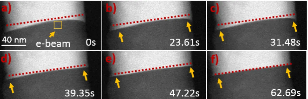
high and low magnification, respectively. Figure 3a-f shows the influence of the electron beam on the Al/Ge binary exchange reaction in the 133 nm Ge NW when it was interacting with the specimen. As indicated by the orange arrow in Figure 3a, the Al migration front had advanced faster at the location where the beam had scanned a small area in previous frames. When the beam then scans a larger area including the entire reaction interface (Figure 3b-f), the difference between the middle front and the two edges becomes smaller, and finally the interface becomes straight again. Similar observations have been reported in the work of Fauske et al. 38 where the thermal diffusion of Au in GaAs
nanowires was studied. Similar to their observations, the beam induced increased replacement rate was limited to the regions near the electron beam exposed area, and did not extend across the entire nanowire cross-section. Therefore, once a step has nucleated, it does not necessarily advance over the entire reaction interface, indicating that the nucleation event is not the rate limiting step of this reaction.
Figure 3. Sequences of HAADF-STEM images were taken while the specimen was being irradiated by the electron beam. a) Image obtained after zooming out from the indicated region. b-f) After decreasing the magnification, the reaction interface is
progressively restored to a flat interface. The yellow arrows indicate the regions far from the more irradiated square indicated in (a). See Supporting Information M4.
Radial and axial propagation of the Al/Ge interface – effect of Al2O3 shell
The diffusion rate could also be affected by other factors; for instance, in the study of Holmberg et al. 39, they have
reported the growth rate dependence on the distance from the metal source. Yaish et al. 14, have showed in the Ni/Si
system that the quality of the nanowire surface determined by the exposure time to ambient air before the metal deposition step could change the growth rate from the square root to the linear time dependence. In the present paper, we present clear evidence of an effect of the NW surface quality on the reaction kinetics and demonstrate that the surface quality can be improved by the presence of a protecting shell. Figure 4a-f represent HAADF-STEM images of Al migration in a 133 nm Ge NW without the presence of an Al2O3 shell. These NWs were exposed to the atmosphere
so that they have been oxidized forming a GeO2 shell (a 3D reconstruction of the GeO2 shell has been reported in the
paper 22). Before starting the heating experiment, the NW was oriented such that the NW Ge(111) growth plane is
parallel to the electron beam to allow better observation of the nucleation phenomena at the Ge(111) reaction interface. Since we observed an influence of the electron beam on the diffusion behaviour at high magnification, which additionally limits the field of view for the observation allowing to see only part of the reaction interface, we decided to lower the magnification for an overview of the exchange reaction of the Al/Ge interface, working at a resolution of 377.5 pm/pixel, just below atomic resolution. HR-STEM images were taken after the propagation had stopped.The Joule heating was started and series of HAADF images were acquired during the exchange reaction. The diffusion behavior in this NW is presented in the supporting information M5. As shown in Figure 4a, the interface of Al-Ge was initially very sharp. After 0.787 s, there was a jump of the Al reaction interface of 6.5 nm in the axial direction at the left side of the NW, corresponding to a replacement of 20 layers of Ge(111) atomic planes. Then the Al/Ge reaction front runs in the lateral direction from the left to right (along the NW diameter of 133 nm) and finishes a cycle after 7.87 s. These observations allow calculating the diffusion speed in the lateral direction to be about 16.9 nm/s. Figure 4g shows the plot of Al protruding length L as a function of time in the axial direction of the propagated NW without having the Al2O3 shell. The graph demonstrates local variations in propagation speed of the Al/Ge reaction front, due
to the nucleation and subsequent ledge flow of steps of a few nm in height on the reaction interface. As can be seen from the plot, the average propagation rate of the reaction interface is about 0.64 nm/s. It is worth noting that the observed growth rate in the axial direction is 26 times smaller than in the lateral direction. This result is quite reasonable since it takes some time to nucleate a new step on the reaction interface. From literature 40, it has been
known that the Ge surface is very sensitive to atmospheric ambience. Probably, the NW surface was strongly oxidized, and this may be related to increased surface roughness and/or the formation of surface defects at the Ge/GeO2
interface (the HAADF STEM and BF STEM images of the Al/Ge interface and a zoom on the oxidation shell are shown in the supporting information S2). Hence the trapping and de-trapping of the reaction interface at these defects could result in the observed stepwise growth. In contrast, investigating the Al/Ge exchange reaction in a Ge NW with the presence of a 5 nm Al2O3 shell, a smoother linear time dependence of the Al diffusion length is observed and plotted
in Figure 4h (see also supporting information M6). The reaction interface speed in this experiment is about 0.143 nm/s. It is worth noting that the diffusion speed in this case is lower than in the example of a NW without the protecting shell (0.64 nm/s). However, we cannot interpret the kinetics between the two NWs since the Joule heating experiments are not temperature calibrated. A high resolution observation of the reaction interface on a different passivated NW is presented in supporting information M7 (BF STEM, dark contrast corresponding to Ge and bright to Al). The movie
shows a precise control of the propagation speed of which the reaction interface advances layer by layer. These results may indicate that in the latter case the quality of the NW surface was better controlled by the protection of the Al2O3
layer, hence the exchange reaction took place uniformly along the NW axial direction without the strong fluctuation of the diffusion rate due to surface defects. A smooth advancement of the interface is paramount for controlling the length of the semiconductor region with atomic scale precision.
Figure 4. a-f) Series of HAADF-STEM images of Al migration in a Ge NW showing the nucleation of a step at the Al/Ge reaction interface and its propagation in the lateral direction from the left to the right. The diameter of the NW is about 133 nm. The yellow dash lines present the step height. The white arrows indicate the positions of the step moving along the reaction interface from the left to the right. Figure 4(g-h) shows the plot of Al converted length L as a function of time in the axial direction of the NW without and with the protection of a 5 nm Al2O3 shell, respectively. The movie of the diffusion presenting the experiment of
Figure 4(a-g) is available for viewing in Supporting Information M5. The experiment presented in Figure 4h is available in the SI M6.
It should be noted that the current study focuses on relatively large diameter NWs (120≤d≤162). Previously we have observed a smooth propagation behavior in much thinner NWs (15≤d≤50) at low temperatures (250 – 330 oC) where
the length of the propagated region as a function of time follows a square root behavior, indicating the reaction is limited by diffusion 22. In addition, using an ex-situ reaction at a heating temperature of 350 oC, it was observed that
no propagation occurs in NW diameters above 150 nm 29. These combined observations potentially indicate that the
reaction rate is limited by diffusion for small NW diameters, and is limited by an interface (either the metal reservoir-NW interface or the reaction interface) for larger diameter reservoir-NWs.
Combining ex-situ and In-situ heating for producing an ultra-small Ge QD
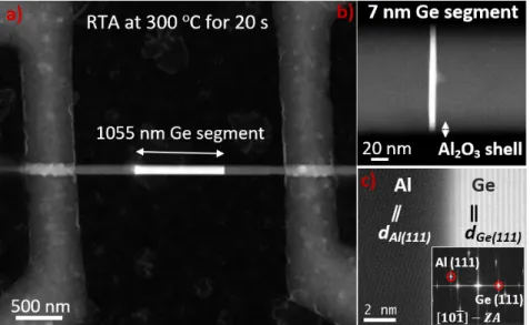
Using the direct Joule heating technique, it is quite difficult to generate the diffusion gently without damaging the heating electrodes. Therefore, we first annealed the sample by RTA to initiate the exchange reaction between Ge and Al. The recipe and characterization by SEM and HAADF STEM combined with chemical mapping by energy dispersive X-ray spectroscopy of the ex-situ annealing process on an Al contacted passivated Ge NW is presented in the supporting information S3. Since the whole sample was heated at the same temperature, no damage was found at the contact pads after the intrusion of Al into the Ge NW. Figure 5a-c represents the HAADF-STEM images of Al incorporation in a 142 nm diameter Ge NW with 5 nm Al2O3 shell, to obtain a smooth advancement of the reaction
interface. The sample was heated at 300 oC for 20 s in N
2 ambience, giving 750 nm propagation length from each side
(Figure 5a). We then performed the direct Joule heating sequentially from each side in-situ in the TEM using HAADF STEM imaging to carefully reduce the unreacted Ge segment length. The image of the Ge segment length at different stages and a movie of the in-situ heating experiment are presented in supporting information S4 and M6, respectively. When the Ge segment reached sub- 10 nm scale, it is important to lower the applied heating voltage to decrease the
diffusion rate until achieving the desired segment length. Since we observe the position of the reaction interface in real time in-situ, we can stop the heating current at any moment. As we use an extremely local heating, the injected power is very small and dissipated almost instantly through the contacts when we remove the heating current. It is this capacity to heat and cool almost instantly that finally allows us to deterministically fabricate a nm sized Ge segment. Figure 5b illustrates the formation of an ultra- small 7 nm Ge segment after a RTA treatment followed by an in-situ Joule heating process. The segment length of this Ge disk was intentionally stopped at 7 nm for further investigations. Due to the relatively large NW diameter, that is much larger than the thickness of this Ge disk, we expect mostly axial confinement in this structure and therefore this structure would resemble a quantum disk. Ge quantum dots could also be reliably fabricated with this method using NWs with smaller diameter. It is also possible to perform a complete Al-Ge exchange for the fabrication of a monocrystalline Al NW 41. Figure 5c shows an HR-HAADF-STEM
image of the interface between the reacted and unreacted part with the corresponding FFT in the inserted figure. The interface appears quite sharp when oriented on the [101&] zone axis of Al. There is a rotation of 18 degrees between the Al(111) atomic planes and Ge(111) planes of the NW growth direction as can be observed in the FFT shown in the inset of Figure 5c. Due to the large difference in lattice constants between Al (aAl= 4.05 Å) and Ge (aGe = 5.65 Å), a rotation at the interface is generally observed, presumably to accommodate the lattice mismatch. We show a schematic of this interface (shown in the supporting information S5). The 18° rotation may be a way for strain minimization and lattice relaxation.
Figure 5. a) HAADF-STEM image of an axial Al/Ge/Al NW hetero-structure formed after the RTA treatment at 300 oC for 20 s. The
NW diameter is about 142 nm and covered by 5 nm Al2O3 shell. b) An ultra- short 7 nm Ge segment was created by combining
RTA and in-situ Joule heating method. c) HR-STEM image with the corresponding FFT at the Al/Ge interface showing the 18 degree rotation between Al(111) and Ge(111) planes when the specimen is oriented on the [101"] direction of observation on the Al part. The interface appears very sharp. See Supporting Information M6.
CONCLUSION
In summary, the diffusion behavior of the Al-Ge thermal exchange reaction was fully described from the earliest stage to the end of the exchange process using real-time observations. We demonstrate all necessary precautions to allow deterministic and reliable fabrication of sub 10 nm Ge quantum dots or disks in a NW, and illustrate this possibility in a proof of principle experiment, creating a semiconductor region with near atomic scale precision between atomically sharp metal contacts. We observed that at magnifications where lattice planes are visible, the electron beam influences the propagation locally at such a high magnification. It is therefore better to work at a slightly lower magnification, with the additional benefit of having the entire reaction interface within the field of view. Importantly, we have demonstrated the influence of the NW surface quality on the diffusion behavior of Al in a Ge NW. Without the presence of a protecting layer, the Al protruding length shows stepwise growth dependence as a function of time while a much smoother linear time dependence is observed when the NW is covered by a 5 nm Al2O3 shell in these relatively large
diameter NWs (120≤d≤162). Finally, combining in-situ and ex-situ heating processes, we have successfully controlled and synthesized an ultrashort Ge segment of nm. From literature, this is the smallest Ge segment length that has been obtained in the Al/Ge binary system, and among the smallest segment in other semiconductor NW metal systems. These atomic -scale observations are extremely useful to understand the reaction behavior of metals with respect to Ge NWs or other semiconductors and observe potential differences with respect to bulk materials.
ABBREVIATIONS:
FETs: field effect transistors; CVD: chemical vapor deposition; VLS: vapor-liquid-solid; NWs: nanowires; ALD: atomic layer deposition; STEM: scanning transmission electron microscope; RTA: rapid thermal annealing; HAADF: high-angle annular dark-field imaging.
ASSOCIATED CONTENT Supporting Information
The Supporting Information is available free of charge at https://pubs.acs.org/doi/10.1021/acsanm.9b02564
S1 shows the degradation of the Al heater by Joule heating technique. S2 shows the surface roughness and/ or the formation of surface defects at the Ge/GeO2 interface. S3 shows the preservation of heating electro- des with ex-situ heating via rapid thermal annealing (RTA). S4 shows HAADF STEM images of the Ge segment length at three different steps: (a) after RTA at 300 °C for 20 s; (b) after first Joule heating using the left heating electrode; and (c) after second Joule heating using the right electrode. S5 shows a schematic illustration of lattice matching between Al(111) and Ge(111) planes without and with 18 degree of rotation between the two plane (PDF)
M1: HAADF STEM image sequence of aluminum incorporation into double Ge NWs (130 and 120 nm in diameter, from the left to the right, respectively) having 5 nm Al2O3 shell (MP4)
M2: HAADF STEM image sequence of Al intruding in 162 nm Ge NW with 5 nm Al2O3 shell by Joule heating method (MP4)
M3: HR HAADF STEM image sequence on the edge of a propagated 133 nm Ge NW without having the protecting shell (MP4)
M4: HAADF STEM image sequence showing a clear influence of the electron beam on the diffusion behavior at the Al/Ge interface (MP4)
M5: HAADF STEM image sequence demonstrating the stepwise diffusion rate in the 133 nm Ge NW without having the protecting shell (MP4)
M6: HAADF STEM image sequence showing the production of an ultra- small Ge segment from the combination of ex-situ and in-ex-situ heating techniques (MP4)
M7: HR BF STEM image sequence of the reaction interface on a passivated NW (dark contrast correspond- ing to Ge and bright to Al) (MP4)
* Competing interests:
The authors declare that they have no competing interests.
AUTHOR INFORMATION Corresponding Author
M. I. Den Hertog − Institut NEEL UPR2940, Grenoble, France; orcid.org/0000-0003-0781-9249; Email: martien.den-hertog@neel.cnrs.fr
Other Authors
M.A. Luong − Université Grenoble Alpes, CEA-Grenoble, Grenoble, France; orcid.org/0000-0002-0876-2400 E. Robin − Université Grenoble Alpes, CEA-Grenoble, Grenoble, France
N. Pauc − Université Grenoble Alpes, CEA-Grenoble, Grenoble, France
P. Gentile − Université Grenoble Alpes, CEA-Grenoble, Grenoble, France; orcid.org/0000-0002-1547-4247 M. Sistani − Technische Universitat Wien, Vienna, Austria; orcid.org/0000-0001-5730-234X
A. Lugstein − Technische Universitat Wien, Vienna, Austria; orcid.org/0000-0001-5693-4775 M. Spies − Institut NEEL UPR2940, Grenoble, France; orcid.org/0000-0002-3570-3422 B. Fernandez − Institut NEEL UPR2940, Grenoble, France
Complete contact information is available at: https://pubs.acs.org/10.1021/acsanm.9b02564
Notes
The authors declare no competing financial interest.
ACKNOWLEDGMENTS
The authors would like to thank Dr. Laurent CAGNON for help on the ALD technique and Dr. Stephane Auffret for help with the Al sputtering. We acknowledge support from the Laboratoire d’excellence LANEF in Grenoble (ANR-10-LABX-51-01). We benefitted from the access to the Nano characterization platform (PFNC) in CEA Minatec Grenoble and Nano-fab from institute NEEL, Grenoble.This project has received funding from the European Research Council (ERC) under the European Union’s Horizon 2020 research and innovation programme (grant agreement N° 758385) for the e-See project. The authors gratefully acknowledge financial support by the Austrian Science Fund (FWF): project No.: P28175-N27.
REFERENCES
(1) Tang, J.; Wang, C.-Y.; Xiu, F.; Zhou, Y.; Chen, L.-J.; Wang, K. L. Formation and Device Application of Ge Nanowire Heterostructures via Rapid Thermal Annealing. Adv. Mater. Sci. Eng. 2011, 2011, 1–16.
https://doi.org/10.1155/2011/316513.
(2) Tang, J.; Wang, C.-Y.; Xiu, F.; Lang, M.; Chu, L.-W.; Tsai, C.-J.; Chueh, Y.-L.; Chen, L.-J.; Wang, K. L. Oxide-Confined Formation of Germanium Nanowire Heterostructures for High-Performance Transistors. ACS Nano
2011, 5 (7), 6008–6015. https://doi.org/10.1021/nn2017777.
(3) Lin, Y.-C.; Lu, K.-C.; Wu, W.-W.; Bai, J.; Chen, L. J.; Tu, K. N.; Huang, Y. Single Crystalline PtSi Nanowires, PtSi/Si/PtSi Nanowire Heterostructures, and Nanodevices. Nano Lett. 2008, 8 (3), 913–918.
https://doi.org/10.1021/nl073279r.
(4) Hu, Y.; Xiang, J.; Liang, G.; Yan, H.; Lieber, C. M. Sub-100 Nanometer Channel Length Ge/Si Nanowire Transistors with Potential for 2 THz Switching Speed. Nano Lett. 2008, 8 (3), 925–930.
https://doi.org/10.1021/nl073407b.
(5) Wu, Y.-T.; Huang, C.-W.; Chiu, C.-H.; Chang, C.-F.; Chen, J.-Y.; Lin, T.-Y.; Huang, Y.-T.; Lu, K.-C.; Yeh, P.-H.; Wu, W.-W. Nickel/Platinum Dual Silicide Axial Nanowire Heterostructures with Excellent Photosensor Applications.
Nano Lett. 2016, 16 (2), 1086–1091. https://doi.org/10.1021/acs.nanolett.5b04309.
(6) Mu, J.; Hou, C.; Wang, H.; Li, Y.; Zhang, Q. Graphene-Carbon Nanotube Papers for Energy Conversion and Storage under Sunlight and Heat. Carbon 2015, 95, 150–156. https://doi.org/10.1016/j.carbon.2015.08.027. (7) Maarouf, A. A.; Kasry, A.; Chandra, B.; Martyna, G. J. A Graphene–Carbon Nanotube Hybrid Material for
Photovoltaic Applications. Carbon 2016, 102, 74–80. https://doi.org/10.1016/j.carbon.2016.02.024.
(8) Björk, M. T.; Knoch, J.; Schmid, H.; Riel, H.; Riess, W. Silicon Nanowire Tunneling Field-Effect Transistors. Appl.
Phys. Lett. 2008, 92 (19), 193504. https://doi.org/10.1063/1.2928227.
(9) Ambhorkar, P.; Wang, Z.; Ko, H.; Lee, S.; Koo, K.; Kim, K.; Cho, D. Nanowire-Based Biosensors: From Growth to Applications. Micromachines 2018, 9 (12), 679. https://doi.org/10.3390/mi9120679.
(10) Zhang, A.; Zheng, G. Semiconductor Nanowires for Biosensors. In Semiconductor Nanowires; Elsevier, 2015; pp 471–490. https://doi.org/10.1016/B978-1-78242-253-2.00017-7.
(11) Minot, E. D.; Kelkensberg, F.; van Kouwen, M.; van Dam, J. A.; Kouwenhoven, L. P.; Zwiller, V.; Borgström, M. T.; Wunnicke, O.; Verheijen, M. A.; Bakkers, E. P. A. M. Single Quantum Dot Nanowire LEDs. Nano Lett. 2007, 7 (2), 367–371. https://doi.org/10.1021/nl062483w.
(12) Yamane, K.; Hamaya, K.; Ando, Y.; Enomoto, Y.; Yamamoto, K.; Sadoh, T.; Miyao, M. Effect of Atomically Controlled Interfaces on Fermi-Level Pinning at Metal/Ge Interfaces. Appl. Phys. Lett. 2010, 96 (16), 162104. https://doi.org/10.1063/1.3368701.
(13) Zhou, Y.; Ogawa, M.; Han, X.; Wang, K. L. Alleviation of Fermi-Level Pinning Effect on Metal/Germanium Interface by Insertion of an Ultrathin Aluminum Oxide. Appl. Phys. Lett. 2008, 93 (20), 202105.
https://doi.org/10.1063/1.3028343.
(14) Yaish, Y. E.; Katsman, A.; Cohen, G. M.; Beregovsky, M. Kinetics of Nickel Silicide Growth in Silicon Nanowires: From Linear to Square Root Growth. J. Appl. Phys. 2011, 109 (9), 094303. https://doi.org/10.1063/1.3574650. (15) Burchhart, T.; Lugstein, A.; Hyun, Y. J.; Hochleitner, G.; Bertagnolli, E. Atomic Scale Alignment of
Copper-Germanide Contacts for Ge Nanowire Metal Oxide Field Effect Transistors. Nano Lett. 2009, 9 (11), 3739–3742. https://doi.org/10.1021/nl9019243.
(16) Dellas, N. S.; Minassian, S.; Redwing, J. M.; Mohney, S. E. Formation of Nickel Germanide Contacts to Ge Nanowires. Appl. Phys. Lett. 2010, 97 (26), 263116. https://doi.org/10.1063/1.3533808.
(17) Liu, B.; Wang, Y.; Dilts, S.; Mayer, T. S.; Mohney, S. E. Silicidation of Silicon Nanowires by Platinum. Nano Lett.
2007, 7 (3), 818–824. https://doi.org/10.1021/nl062393r.
(18) Dayeh, S. A.; Mack, N. H.; Huang, J. Y.; Picraux, S. T. Advanced Core/Multishell Germanium/Silicon Nanowire Heterostructures: The Au-Diffusion Bottleneck. Appl. Phys. Lett. 2011, 99 (2), 023102.
https://doi.org/10.1063/1.3567932.
(19) Chou, Y.-C.; Wu, W.-W.; Cheng, S.-L.; Yoo, B.-Y.; Myung, N.; Chen, L. J.; Tu, K. N. In-Situ TEM Observation of Repeating Events of Nucleation in Epitaxial Growth of Nano CoSi 2 in Nanowires of Si. Nano Lett. 2008, 8 (8),
2194–2199. https://doi.org/10.1021/nl080624j.
(20) Izumi, T.; Taniguchi, M.; Kumai, S.; Sato, A. Ferromagnetic Properties of Cyclically Deformed Fe 3 Ge and Ni 3
(21) Jamet, M.; Barski, A.; Devillers, T.; Poydenot, V.; Dujardin, R.; Bayle-Guillemaud, P.; Rothman, J.; Bellet-Amalric, E.; Marty, A.; Cibert, J.; Mattana, R.; Tatarenko, S. High-Curie-Temperature Ferromagnetism in Self-Organized Ge1−xMnx Nanocolumns. Nat. Mater. 2006, 5, 653.
(22) El hajraoui, K.; Luong, M. A.; Robin, E.; Brunbauer, F.; Zeiner, C.; Lugstein, A.; Gentile, P.; Rouvière, J.-L.; Den Hertog, M. In Situ Transmission Electron Microscopy Analysis of Aluminum–Germanium Nanowire Solid-State Reaction. Nano Lett. 2019, 19 (5), 2897–2904. https://doi.org/10.1021/acs.nanolett.8b05171.
(23) Sistani, M.; Staudinger, P.; Greil, J.; Holzbauer, M.; Detz, H.; Bertagnolli, E.; Lugstein, A. Room-Temperature Quantum Ballistic Transport in Monolithic Ultrascaled Al–Ge–Al Nanowire Heterostructures. Nano Lett. 2017,
17 (8), 4556–4561. https://doi.org/10.1021/acs.nanolett.7b00425.
(24) Staudinger, P.; Sistani, M.; Greil, J.; Bertagnolli, E.; Lugstein, A. Ultrascaled Germanium Nanowires for Highly Sensitive Photodetection at the Quantum Ballistic Limit. Nano Lett. 2018, 18 (8), 5030–5035.
https://doi.org/10.1021/acs.nanolett.8b01845.
(25) Sistani, M.; Delaforce, J.; Kramer, R. B. G.; Roch, N.; Luong, M. A.; den Hertog, M. I.; Robin, E.; Smoliner, J.; Yao, J.; Lieber, C. M.; Naud, C.; Lugstein, A.; Buisson, O. Highly Transparent Contacts to the 1D Hole Gas in
Ultrascaled Ge/Si Core/Shell Nanowires. ACS Nano 2019, acsnano.9b06809. https://doi.org/10.1021/acsnano.9b06809.
(26) Vigneau, F.; Mizokuchi, R.; Zanuz, D. C.; Huang, X.; Tan, S.; Maurand, R.; Frolov, S.; Sammak, A.; Scappucci, G.; Lefloch, F.; Franceschi, S. Germanium Quantum-Well Josephson Field-Effect Transistors and Interferometers.
Nano Lett. 2019, 19 (2), 1023–1027. https://doi.org/10.1021/acs.nanolett.8b04275.
(27) Mongillo, M.; Spathis, P.; Katsaros, G.; Gentile, P.; Sanquer, M.; De Franceschi, S. Joule-Assisted Silicidation for Short-Channel Silicon Nanowire Devices. ACS Nano 2011, 5 (9), 7117–7123.
https://doi.org/10.1021/nn202524j.
(28) Sistani, M.; Luong, M. A.; den Hertog, M. I.; Robin, E.; Spies, M.; Fernandez, B.; Yao, J.; Bertagnolli, E.; Lugstein, A. Monolithic Axial and Radial Metal–Semiconductor Nanowire Heterostructures. Nano Lett. 2018, 18 (12), 7692–7697. https://doi.org/10.1021/acs.nanolett.8b03366.
(29) Kral, S.; Zeiner, C.; Stöger-Pollach, M.; Bertagnolli, E.; Den Hertog, M. I.; Lopez-Haro, M.; Robin, E.; El Hajraoui, K.; Lugstein, A. Abrupt Schottky Junctions in Al/Ge Nanowire Heterostructures. Nano Lett. 2015, 15 (7), 4783– 4787. https://doi.org/10.1021/acs.nanolett.5b01748.
(30) Den Hertog, M. I.; González-Posada, F.; Songmuang, R.; Rouviere, J. L.; Fournier, T.; Fernandez, B.; Monroy, E. Correlation of Polarity and Crystal Structure with Optoelectronic and Transport Properties of GaN/AlN/GaN Nanowire Sensors. Nano Lett. 2012, 12 (11), 5691–5696. https://doi.org/10.1021/nl302890f.
(31) Den Hertog, M.; Donatini, F.; McLeod, R.; Monroy, E.; Sartel, C.; Sallet, V.; Pernot, J. In Situ Biasing and off-Axis Electron Holography of a ZnO Nanowire. Nanotechnology 2018, 29 (2), 025710. https://doi.org/10.1088/1361-6528/aa923c.
(32) JipelecTM Jetfirst: Compact & Robust RTP Furnace. Http://Www.Ecm-Usa.Com/Products/Rtp-Furnaces/Jetfirst
(33) Wildfire Nano-Chip. DENSsolutions. Https://Denssolutions.Com/Products/Wildfire/Nano-Chip/
(34) Kordic, S.; Augur, R. A.; Dirks, A. G.; Wolters, R. A. M. Stress Voiding and Electromigration Phenomena in Aluminum Alloys. Appl. Surf. Sci. 1995, 91 (1–4), 197–207. https://doi.org/10.1016/0169-4332(95)00119-0. (35) Castaño, E.; Maiz, J.; Flinn, P.; Madden, M. In Situ Observations of Dc and Ac Electromigration in Passivated Al
Lines. Appl. Phys. Lett. 1991, 59 (1), 129–131. https://doi.org/10.1063/1.105551.
(36) Kondo, S.; Ogasawara, K.; Hinode, K. Thermographic Analysis of Electromigration Phenomena in Aluminum Metallization. J. Appl. Phys. 1996, 79 (2), 736. https://doi.org/10.1063/1.360819.
(37) Loferski, J. J.; Rappaport, P. Radiation Damage in Ge and Si Detected by Carrier Lifetime Changes: Damage Thresholds. Phys. Rev. 1958, 111 (2), 432–439. https://doi.org/10.1103/PhysRev.111.432.
(38) Fauske, V. T.; Huh, J.; Divitini, G.; Dheeraj, D. L.; Munshi, A. M.; Ducati, C.; Weman, H.; Fimland, B.-O.; van Helvoort, A. T. J. In Situ Heat-Induced Replacement of GaAs Nanowires by Au. Nano Lett. 2016, 16 (5), 3051– 3057. https://doi.org/10.1021/acs.nanolett.6b00109.
(39) Holmberg, V. C.; Collier, K. A.; Korgel, B. A. Real-Time Observation of Impurity Diffusion in Silicon Nanowires.
Nano Lett. 2011, 11 (9), 3803–3808. https://doi.org/10.1021/nl201879u.
(40) Loscutoff, P. W.; Bent, S. F. REACTIVITY OF THE GERMANIUM SURFACE: Chemical Passivation and Functionalization. Annu. Rev. Phys. Chem. 2006, 57 (1), 467–495.
(41) Brunbauer, F. M.; Bertagnolli, E.; Majer, J.; Lugstein, A. Electrical Transport Properties of Single-Crystal Al Nanowires. Nanotechnology 2016, 27 (38), 385704. https://doi.org/10.1088/0957-4484/27/38/385704.