HAL Id: hal-03015494
https://hal.archives-ouvertes.fr/hal-03015494
Submitted on 7 Dec 2020HAL is a multi-disciplinary open access archive for the deposit and dissemination of sci-entific research documents, whether they are pub-lished or not. The documents may come from teaching and research institutions in France or abroad, or from public or private research centers.
L’archive ouverte pluridisciplinaire HAL, est destinée au dépôt et à la diffusion de documents scientifiques de niveau recherche, publiés ou non, émanant des établissements d’enseignement et de recherche français ou étrangers, des laboratoires publics ou privés.
Impact of Nitrogen on the Crystallization and
Microstructure of Ge-Rich GeSbTe Alloys
Minh Anh Luong, Dingfang Wen, Eloïse Rahier, Nicolas Ratel-Ramond,
Béatrice Pécassou, Alain Claverie, Yannick Le Friec, Daniel Benoit
To cite this version:
Minh Anh Luong, Dingfang Wen, Eloïse Rahier, Nicolas Ratel-Ramond, Béatrice Pécassou, et al.. Impact of Nitrogen on the Crystallization and Microstructure of Ge-Rich GeSbTe Alloys. physica status solidi (RRL) - Rapid Research Letters, Wiley-VCH Verlag, In press, pp.2000443. �10.1002/pssr.202000443�. �hal-03015494�
1
Impact of Nitrogen on the Crystallization and Microstructure of Ge-Rich GeSbTe Alloys
Minh Anh Luong, Dingfang Wen, Eloïse Rahier, Nicolas Ratel Ramond, Béatrice Pecassou, Yannick Le Friec, Daniel Benoit and Alain Claverie*
Dr. Minh Anh Luong, Dingfang Wen, Eloïse Rahier, Dr. Nicolas Ratel Ramond, Béatrice Pecassou, Prof. A. Claverie
CEMES-CNRS 29 Rue Jeanne Marvig 31055 Toulouse, France.
E-mail: minh-anh.luong@cemes.fr, claverie@cemes.fr Yannick Le Friec, Dr. Daniel Benoit
STMicroelectronics 850 Rue Jean Monnet 38920 Crolles, France. E-mail: daniel.benoit@st.com
Keywords: phase change materials, N-doped Ge-rich GST, crystallization, segregation
Abstract:
We report the influence of N concentration on the crystallization kinetics, microstructural evolution, and composition of Ge-rich GeSbTe (GST) alloys during thermal annealing by using X-ray diffraction and scanning and transmission electron microscopy. We show that the incorporation of N in Ge-rich GST tends to slow down the phase separation, crystallization, and growth processes during annealing. This can be attributed to the reduced diffusivity of Ge, which interacts and quickly bonds with N. Technological advantages of N doping are also discussed, considering the increased stability of the amorphous phase with respect to its parent crystalline phase, finer microstructure, flatness of the GST films after crystallization, and disappearance of the low-resistivity hexagonal phase at high temperature.
2
INTRODUCTION
Among different phase-change materials (PCM), the Ge2Sb2Te5 alloy (GST-225) has been arguably the most studied system in research and development. 1–3 Prominent variations in its physical properties, such as optical reflectance and electrical resistivity, driven by its structural change from amorphous to crystalline states, have been exploited in various memory devices, such as CD ROMs and mass-storage electrical memories. In phase-change memories, reversible SET-to-RESET transitions are obtained by feeding a direct current to the cell and heating the material in a small dome with a diameter of a few tens of nanometers to crystallize it or to quench it from the melt. However, GST-225 has several characteristics, such as a low crystallization temperature in the range 120–150 °C and the development of a less resistive hexagonal phase at high temperature (330–350 °C), which severely limit its application prospects in different fields.
Similar to many other systems, suitable chemical doping is also a popular method to engineer the properties of GST-225. For example, N doping has been reported to significantly affect various characteristics of GST-225, such as an initial increase in its crystallization temperature while reducing its kinetics and generating smaller crystalline grains in the GST layers. 4,5 The increased thermal stability of the amorphous GST-225 was also proposed due to the presence of atomic and molecular N in interstitial sites and its favored bonding with Ge. 6,7 The propensity of this bonding between N and Ge results in reduced Ge diffusivity, which has been revealed by many studies explaining the subsequent changes in different properties. 8-10 Increasing Ge content in the deposited (amorphous) layers was also found to increase the crystallization temperature up to 380 °C for GST-based alloys, 11 making it suitable for different applications. The optimized combination of N doping and increased Ge content has been recently proved to enhance the stability of the amorphous (RESET) phase, providing better contrast between the two states and very good electrical characteristics. 12–17
3
Recently, the crystallization characteristics and resulting microstructural evolutions of such optimized N-doped Ge-rich GST alloys have been reported in detail. 18 However, the influence of N concentration on these characteristics has not been studied yet. To this end, we report the impact of N concentration on the microstructure, composition, and surface morphologies of N-doped Ge-rich GST alloys during thermal annealing by using X-ray diffraction (XRD), scanning electron microscopy (SEM), and transmission electron microscopy (TEM).
EXPERIMENTAL
Ge enriched GST thin films (thickness: 100 nm, CGe > 30%) containing different N concentrations (0, 2, 6.5, and 10 at.%) were grown by the physical vapor deposition method on 300 mm silicon (100) wafers using an industrial tool. These N-doped Ge-rich GST films were named as NGGST. The NGGST films were first capped with an ultra-thin (14 Å) Ti-rich TiN layer and then a 20 nm-thick TiN layer to protect the layers from oxidation. Specimens cut from the wafers were annealed in a horizontal Carbolite furnace under atmospheric pressure and N2 gas flow at temperatures ranging from 340 to 500 °C and for durations ranging from a few minutes to several hours. XRD measurements were carried out using a Bruker D8 Discover diffractometer with a μS-Co source (λ = 1.789 Å) and a 2D Vantec 500 detector, in the grazing incidence mode, where the glancing angle was 0.5°. Surface images of the samples were acquired by an SEM using secondary electrons. Samples for cross-sectional TEM images were prepared by FIB using an FEI Helios NanoLab 600 operating with a 30 keV Ga ion beam. Samples were finally polished and cleaned at 2 keV. Conventional TEM imaging and STEM-EDX (Energy-dispersive X-ray spectroscopy) analyses were performed using a Philips CM20-FEG TEM equipped with a Microanalyzer QUANTAX XFlash detector with a 30 mm2 active area providing an energy resolution of 127 eV.
4
RESULTS
Figure 1 shows four sets of XRD patterns obtained for the NGGST films with different N
concentrations (0, 2, 6.5, and 10 at.%) annealed at different temperatures for different durations (340 and 380 °C for 3 h, and 400, 450, and 500 °C for 30 min). Undoped GGST film (0%), annealed at 340 °C for 3 h, exhibited broad diffraction peaks centered at the 2θ values expected for the cubic Ge and FCC-GST-225 phases (Figure 1a), and higher annealing temperatures than 380 °C did not change these characteristics significantly. However, as the temperature increased from 400 to 500 °C, the Ge peak became more intense and narrower. In addition, the developing shoulder found at 2θ ≈ 34° with increasing temperature corresponded to a characteristic peak of the HEX-GST-225 phase, which coexisted with the cubic phase as a minor component.
In the case of 2% N-doping, the above features were present, although Ge peaks were broader than those found in the undoped GGST films annealed at similar conditions. In addition, a large shoulder appeared instead of a distinct peak from the HEX-GST-225 phase at 2θ ≈ 34°. A similar feature was observed when the doping concentration was 6.5%. The hexagonal phase could only be detected by the small shoulder appeared close to the characteristic peak of the cubic GST-225 phase in the sample annealed at 450 °C for 30 min. The Ge peaks were broader than those in the undoped GGST film, and most importantly, the crystallization of any of these two phases did not occur after the 340 °C/3 h annealing process. Finally, in the sample containing 10 at.% N, crystallization started at 400 °C, with the selective crystallization of the Ge phase (very broad peaks) followed by the crystallization of the cubic GST-225 phase after the annealing at 450 °C. Moreover, when annealed at 500 °C, the characteristic peaks from the two phases were found to be very broad than those observed in the undoped GGST film. The above results describe the impact of N-doping on the crystallization of GGST films. Higher thermal budgets are needed to produce N-doped materials with crystalline characteristics
5
similar to the undoped GGST system. While the crystallization sequence remained unchanged, that is, the crystallization of GST-225 followed the crystallization of the Ge phase, the kinetics of this complex process was modified by the presence of N. The fact that the development of the hexagonal phase of GST-225 weakened as the N content increased may also be related to the evolving kinetic factors when the annealing duration was limited to 30 min at 500 °C. Moreover, higher N concentrations resulted in broader diffraction peaks, particularly for the characteristic peak from the Ge cubic phase. This must be attributed to the increased difficulty for the small Ge grains to coalesce with high N concentrations. 16
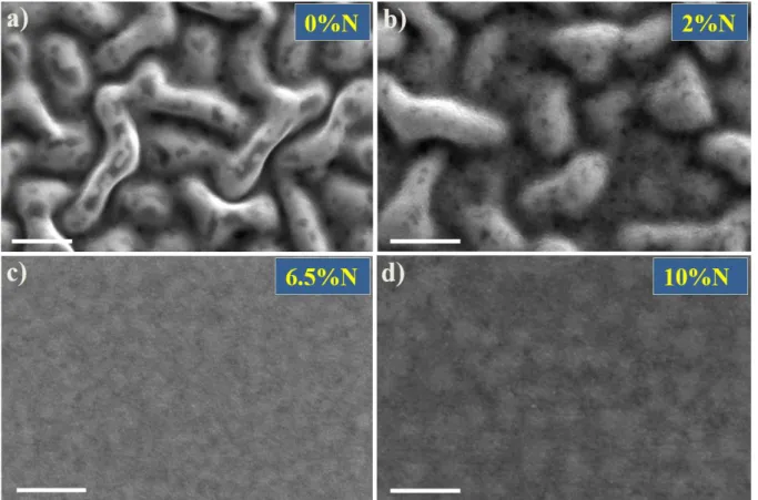
Figure 2 shows the surface SEM micrographs for different NGGST samples after
annealing at 500 °C for 30 min. SEM images of the as-deposited GGST and 10% NGGST films are presented in Supporting Information S1, showing a flat surface morphology before annealing. Interestingly, the surfaces of the undoped and 2% NGGST films showed distinct “spaghetti-like” features similar to those typically found in systems undergone spinodal phase separations. 19 Moreover, dark contrasting features of lengths of approximately tens of nanometers were observed within the cores of those spaghettis. In contrast, the samples with higher N contents (6.5 and 10%) showed flat surfaces, featuring weakly contrasting regions. As the films were flat, these contrasts (Figure 2d) can be attributed to the compositional variations within the NGGST layer underneath the 20 nm TiN capping layer. The deviations in the surface roughness and compositional homogeneity manifested drastic color variations when observed under white light illumination (shown in Supporting Information S2).
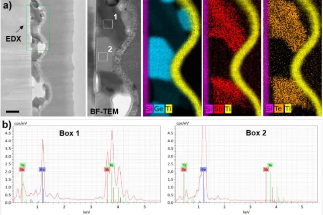
Figure 3 shows the cross-sectional bright-field TEM (BF-TEM) images and respective
EDX chemical maps obtained for the undoped GGST film (a), including the spectrum analyses on different areas of the specimen (b). The distributions of Si, Ge, Sb, and Te are displayed in pink, blue, red, and orange, respectively. Nitrogen maps are not displayed as the signal overlap between the K-line (N) and L-line (Sb) resulted in poor resolving power. The BF-TEM images in Figure 3a shows that the N-free GGST film is highly inhomogeneous. Bumps and valleys
6
were observed on the surface, with dimensions corresponding to the spaghettis observed by the SEM. Notably, voids were systematically present on the top regions of the bumps, which complemented the black features seen in the SEM images. The spectrum analysis shown in
Figure 3b and the EDX quantification presented in Supporting Information section III showed
that large Ge crystals were formed within the thinnest regions (valleys) of the system, while GST crystals were formed in the thickest parts (bumps) of the system along with the voids. These observations confirmed that the surface morphologies of the undoped or lightly doped samples were determined by the chemical phase separations of the alloys.
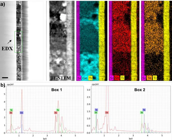
In contrast, Figure 4 shows that the 10% N-doped NGGST film remained flat after annealing. Although phase separations led to alternating Ge-rich and GST-rich regions of similar dimensions, it did not contribute to surface deformations as confirmed by the SEM results. Both the Ge and GST-225 grains were tiny, and they did not coalesce as indicated by the XRD results shown in Figure 1d. Moreover, voids were observed, but in smaller concentrations and smaller dimensions than those found in the undoped GGST sample.
DISCUSSION AND CONCLUSIONS
First, this study confirms the primary findings by Agati et al., 18 which suggested that the complete crystallization of GGST systems with and without N-doping occurs through successive steps, segregation, and the crystallization of Ge is followed by the crystallization of the cubic GST-225 phase. We further demonstrated that the incorporation of N significantly affects the crystallization process and the microstructures of the layers.
We observed that the crystallization occurred at higher temperatures as the N content in the alloy increased. Second, we found that the hexagonal GST-225 phase became the major component in the undoped GGST layer after annealing at 500 °C for 30 min, whereas it was a minor component in the 2% and 6.5% N-doped layers. However, the hexagonal phase was not
7
detected at all in the 10% N-doped sample annealed under similar conditions. These two observations suggested that the main consequence of the N-doping was slowing down of the different mechanisms that drive the crystallization and phase transitions of the GGST layers. As a result, with the increase in N-doping concentration in the GGST film, more thermal energy was needed to reach approximately the same crystalline state for the system. We infer that this sluggish crystallization process was induced by the reduced diffusivity of Ge in the presence of N due to the formation of Ge-N bonds.
Another important effect of N-doping was the inhibition of the coalescence of the Ge and GST grains during annealing. In the case of undoped GGST, the XRD patterns showed that the Ge grains were larger (the peaks were narrower) when the thermal budget increased. In contrast, in the 10 % NGGST sample, the grains were initially much smaller and did not produce large sizes even after high-temperature annealing, which was also confirmed by TEM. The grains in the undoped GGST layer appeared with dimensions similar to the layer thickness after annealing at 500 °C, while they were tiny (few tens of nanometers) in the 10 % NGGST layer even after the same annealing process was conducted.
The TEM results proved that the phase separations were driven by the high-temperature annealing processes (500 °C). Alternating Ge and GST regions with similar widths of the order of several hundreds of nanometers were formed irrespective of the N-doping concentration. However, the undoped layer exhibited surface undulations, where the top regions were mostly made of GST-225 and large voids, while the heavily doped layers remained flat. Although further detailed investigations are still needed, we speculate that the observed surface morphologies are partly driven by the fast thermal evolution of the undoped material. Owing to the high diffusivities and differences between the surface and interface energies, GST grains in the cubic phase grew to the point where their heights became larger than the initial thickness of the as-deposited amorphous film. Consequently, the TiN layer was plastically deformed to follow the shapes of the grains. Later on, after the high-temperature annealing for longer
8
durations, the cubic grains transformed into the hexagonal phase. In this process, the material produced a large number of vacancies (10% in atomic number), which probably merged to form large voids detected above or below the GST grains. In contrast, in heavily doped materials, the grain growths were inhibited by the reduced element diffusivities in the heavily doped materials. The grains were small, and the layer remained flat. Although voids were found, they were small and randomly distributed in the layer. We infer that these voids were generated during the crystallization of the layer when the volume occupied by the two phases decreased by 6–7% for GST-225 20 and 2–3% for Ge. Indeed, the homogeneous and randomized nucleations of the crystalline grains enforced local densification within the material, which must be locally compensated by the void formation.
In summary, we showed that the incorporation of N in the GGST system tends to slow down the phase separation and crystallization processes, promoting the need to increase the thermal budget to obtain material characteristics similar to those of the undoped systems. This can be attributed to the reduced diffusivity of Ge caused by the interactions and bonding with N atoms.
Nevertheless, from the technological perspective, N doping of GGST can in fact offer several advantages. The reduced crystallization rate and growth kinetics ensure increased stability of the amorphous phase with respect to its parent crystalline phase. Moreover, N doping can ensure that the films remain flat after the thermal crystallization. Another important factor is that the smaller grains found in NGGST systems would result in low melting temperature and better homogeneity of the electrical and optical properties when probed locally. Finally, we also noted that N doping can effectively suppress the transformations of the FCC-GST-225 phase to the hexagonal phase, where the latter is often not desirable because of its extremely low resistivity.
9
DECLARATION OF COMPETING INTEREST
The authors declare that they have no known competing financial interests.
ACKNOWLEDGMENT
This work is part of the “Ô-GST Project” and partially funded by the nano2022 (IPCEI) initiative and by the ST/CNRS Action on GST materials.
10
REFERENCES
(1) Raoux, S.; Wełnic, W.; Ielmini, D. Phase Change Materials and Their Application to Nonvolatile Memories. Chem. Rev. 2010, 110 (1), 240–267.
(2) Noé, P.; Vallée, C.; Hippert, F.; Fillot, F.; Raty, J.-Y. Phase-Change Materials for Non-Volatile Memory Devices: From Technological Challenges to Materials Science Issues. Semicond. Sci. Technol. 2018, 33 (1), 013002.
(3) Guo, P.; Sarangan, A.; Agha, I. A Review of Germanium-Antimony-Telluride Phase Change Materials for Non-Volatile Memories and Optical Modulators. Appl. Sci. 2019, 9 (3), 530.
(4) Shelby, R. M.; Raoux, S. Crystallization Dynamics of Nitrogen-Doped Ge2Sb2Te5. J.
Appl. Phys. 2009, 105 (10), 104902.
(5) Lai, Y.; Qiao, B.; Feng, J.; Ling, Y.; Lai, L.; Lin, Y.; Tang, T.; Cai, B.; Chen, B.
Nitrogen-Doped Ge2Sb2Te5 Films for Nonvolatile Memory. J. Electron. Mater. 2005, 34 (2), 176–181.
(6) Kim, K.-H.; Park, J.-C.; Lee, J.-H.; Chung, J.-G.; Heo, S.; Choi, S.-J. Nitrogen-Doping Effect on Ge2Sb2Te5 Chalcogenide Alloy Films during Annealing. Jpn. J. Appl. Phys.
2010, 49 (10), 101201.
(7) Kim, Y.; Baeck, J. H.; Cho, M.-H.; Jeong, E. J.; Ko, D.-H. Effects of N2+ Ion Implantation on Phase Transition in Ge2Sb2Te5 Films. J. Appl. Phys. 2006, 100 (8), 083502.
(8) Fillot, F.; Sabbione, C.; Pierre, F.; Hippert, F.; Noé, P. Crystallization of Ge2Sb2Te5 and Nitrogren-Doped Ge2Sb2Te5 Phase-Change-Materials Thin Films Studied by in Situ Combined X-Ray Scattering Techniques. J. Appl. Crystallogr. 2018, 51 (6), 1691–1705. (9) Jung, M.-C.; Lee, Y. M.; Kim, H.-D.; Kim, M. G.; Shin, H. J.; Kim, K. H.; Song, S. A.;
Jeong, H. S.; Ko, C. H.; Han, M. Ge Nitride Formation in N-Doped Amorphous Ge2Sb2Te5. Appl. Phys. Lett. 2007, 91 (8), 083514.
(10) Lee, T. H.; Loke, D.; Elliott, S. R. Microscopic Mechanism of Doping-Induced
Kinetically Constrained Crystallization in Phase-Change Materials, Adv. Mater. 2015, 27, 5477–5483.
(11) Zuliani, P.; Varesi, E.; Palumbo, E.; Borghi, M.; Tortorelli, I.; Erbetta, D.; Libera, G. D.; Pessina, N.; Gandolfo, A.; Prelini, C.; Ravazzi, L.; Annunziata, R. Overcoming
Temperature Limitations in Phase Change Memories With Optimized GexSbyTez. IEEE
Trans. Electron Devices 2013, 60 (12), 4020–4026.
(12) Cheng, H. Y.; Wu, J. Y.; Cheek, R.; Raoux, S.; BrightSky, M.; Garbin, D.; Kim, S.; Hsu, T. H.; Zhu, Y.; Lai, E. K.; Joseph, E.; Schrott, A.; Lai, S. C.; Ray, A.; Lung, H. L.; Lam, C. A Thermally Robust Phase Change Memory by Engineering the Ge/N Concentration in (Ge, N)xSbyTez Phase Change Material. International Electron Devices Meeting; IEEE: San Francisco, CA, USA, 2012, p 31.1.1-31.1.4.
11
(13) Navarro, G.; Coue, M.; Kiouseloglou, A.; Noe, P.; Fillot, F.; Delaye, V.; Persico, A.; Roule, A.; Bernard, M.; Sabbione, C.; Blachier, D.; Sousa, V.; Perniola, L.; Maitrejean, S.; Cabrini, A.; Torelli, G.; Zuliani, P.; Annunziata, R.; Palumbo, E.; Borghi, M.; Reimbold, G.; De Salvo, B. Trade-off between SET and Data Retention Performance Thanks to Innovative Materials for Phase-Change Memory. IEEE International Electron Devices Meeting; IEEE: Washington, DC, USA, 2013, p 21.5.1-21.5.4.
(14) Kiouseloglou, A.; Navarro, G.; Sousa, V.; Persico, A.; Roule, A.; Cabrini, A.; Torelli, G.; Maitrejean, S.; Reimbold, G.; De Salvo, B.; Clermidy, F.; Perniola, L. A Novel Programming Technique to Boost Low-Resistance State Performance in Ge-Rich GST Phase Change Memory. IEEE Trans. Electron Devices 2014, 61 (5), 1246–1254. (15) Zuliani, P.; Palumbo, E.; Borghi, M.; Dalla Libera, G.; Annunziata, R. Engineering of
Chalcogenide Materials for Embedded Applications of Phase Change Memory. Solid-State Electron. 2015, 111, 27–31.
(16) Navarro, G.; Sousa, V.; Noé, P.; Castellani, N., Coué, M.; Kluge, J.; Kiouseloglou, A.; Sabbione, C.; Persico, A.; Roule, A.; Cueto, O.; Blonkowski, S.; Fillot, F.; Bernier, N.; Annunziata, R.; Borghi, M.; Palumbo, E.; Zuliani, P. and L. Perniola, N-doping Impact in Optimized Ge-rich Materials Based Phase-Change Memory. IEEE 8th International
Memory Workshop (IMW) 2016, p 1–4.
(17) Bourgine, A.; Grisolia, J.; Vallet, M.; Benoit, D.; Le Friec, Y.; Caubet-Hilloutou, V.; Claverie, A. On the Charge Transport Mechanisms in Ge-Rich GeSbTe Alloys. Solid-State Electron. 2020, 172, 107871.
(18) Agati, M.; Vallet, M.; Joulié, S.; Benoit, D.; Claverie, A. Chemical Phase Segregation during the Crystallization of Ge-Rich GeSbTe Alloys. J. Mater. Chem. C 2019, 7 (28), 8720–8729.
(19) Sofonea, V.; Mecke, K. R. Morphological Characterization of Spinodal Decomposition Kinetics. Eur. Phys. J. B 1999, 8 (1), 99–112.
(20) Njoroge, W. K.; Wöltgens, H.-W.; Wuttig, M. Density Changes upon Crystallization of Ge2Sb2.04Te4.74 Films. J. Vac. Sci. Technol. Vac. Surf. Films 2002, 20 (1), 230–233.
12
Figure 1. XRD patterns of NGGST films containing different N concentrations. (a) Undoped
system, and (b-d) with 2, 6.5, and 10 at.% of N, respectively, annealed at different
temperatures for different durations in N2 ambient as mentioned in the header. The vertical lines with filled red squares, green triangles and blue diamonds show the expected 2θ positions of the diffraction peaks corresponding to the Ge (111), GST-225 hexagonal (013), and GST-225 FCC (200) planes, respectively.
13
Figure 2. SEM micrographs of the surface of NGGST films containing different N doping
concentrations: (a) Undoped film and (b-d) doped films with 2, 6.5, and 10 at.% of N, respectively, annealed at 500 °C for 30 min in N2 atmosphere. The white scale bars refer to a length of 500 nm.
14
Figure 3. (a) BF-TEM images and corresponding EDX maps of an undoped GGST film,
annealed at 500 °C for 30 min. (b) Spectrum analysis for two different regions of the GGST film (indicated by the dotted square boxes 1 and 2 on the BF-TEM image). The black scale bar refers to a length of 150 nm.
15
Figure 4. (a) BF-(S)TEM images and corresponding EDX maps of a 10% NGGST film,
annealed at 500 °C for 30 min. (b) Spectrum analysis on two different regions of the NGGST film (indicated by the dotted square boxes 1 and 2 on the BF-(S)TEM image). The black scale bar refers to a length of 150 nm.