Publisher’s version / Version de l'éditeur:
Advanced luminescent materials and quantum confinement II : proceedings of the
International Symposium, pp. 195-202, 2002
READ THESE TERMS AND CONDITIONS CAREFULLY BEFORE USING THIS WEBSITE. https://nrc-publications.canada.ca/eng/copyright
Vous avez des questions? Nous pouvons vous aider. Pour communiquer directement avec un auteur, consultez la première page de la revue dans laquelle son article a été publié afin de trouver ses coordonnées. Si vous n’arrivez pas à les repérer, communiquez avec nous à [email protected].
Questions? Contact the NRC Publications Archive team at
[email protected]. If you wish to email the authors directly, please see the first page of the publication for their contact information.
NRC Publications Archive
Archives des publications du CNRC
This publication could be one of several versions: author’s original, accepted manuscript or the publisher’s version. / La version de cette publication peut être l’une des suivantes : la version prépublication de l’auteur, la version acceptée du manuscrit ou la version de l’éditeur.
Access and use of this website and the material on it are subject to the Terms and Conditions set forth at
Electroluminescence stabilization of nanocrystalline porous silicon
diodes
Koshida, N.; Kadokura, J.; Gelloz, B.; Boukherroub, R.; Wayner, D. M.;
Lockwood, D. J.
https://publications-cnrc.canada.ca/fra/droits
L’accès à ce site Web et l’utilisation de son contenu sont assujettis aux conditions présentées dans le site LISEZ CES CONDITIONS ATTENTIVEMENT AVANT D’UTILISER CE SITE WEB.
NRC Publications Record / Notice d'Archives des publications de CNRC:
https://nrc-publications.canada.ca/eng/view/object/?id=99b79596-5074-4b58-8f15-eba0bf98fbf3 https://publications-cnrc.canada.ca/fra/voir/objet/?id=99b79596-5074-4b58-8f15-eba0bf98fbf3
ELECTROLUMINESCENCE STABILIZATION OF NANOCRYSTALLINE POROUS SILICON DIODES
N. Koshida, J. Kadokura, B. Gelloz
Dpt. Electrical and Electronic Eng., Tokyo Univ. of A&T Koganei, Tokyo 184-8588, Japan
R. Boukherroub, D.M. Wayner, and D.J. Lockwood National Research Council, Ottawa, Canada K1A 0R6
1. Introduction
For practical applications of electroluminescence (EL) from nanocrystalline porous silicon (nc-PS) diodes [1], the external power efficiency (EPE) should be improved beyond 1% at operating voltages below 10 V and the stability longer than 10,000 h under a cw operation. We recently developed a PS-EL device which offers the red band emission with an EPE of 0.4% at a voltage of 5 V [2], an external quantum efficiency (EQE) of 1.1% [3]. The remaining subject to be pursued further is to enhance the EL stability. For this purpose, there are two possible approaches: (a) encapsulation of the device surface by a water-proof thin film and (b) passivation of luminescent nc-Si surfaces themselves by a stable termination. The effectiveness of the former was demonstrated in our previous paper [4]. In this paper, it is reported that the latter is also very useful for stabilizing the EL emission.
2. Experiments
The EL device is composed of a semitransparent indium tin oxide (ITO) top contact, a nc-PS layer treated by electrochemical oxidation (ECO), an n+-type Si (111) wafer, and an ohmic back contact. The post-anodization ECO produces a significant improvement in the EL efficiency [5]. To stabilize the ECO-treated nc-PS, the additional chemical functionalization by 1-decene [6] is employed along the following process.
(a) Cleaning in a buffered HNO3+HF solution.
(b) Photoanodization by a sequential current modulation scheme such that a thin compact superficial layer (200 nm in thickness) and an active layer (800 nm thick) is formed on the outer surface and the bulk, respectively.
(c) ECO treatment in a 1N H2SO4 solution for a time at
which the electrochemical EL reaches a maximum. (d) Chemical functionalization for 1 h at a temperature of 90 in 1-decene CH3(CH2)7CH: CH2.
(e) Top contact formation by rf-sputtering deposition of a thin ITO film (300 nm in thickness).
3. Results and Discussion
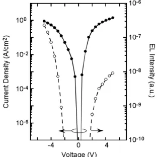
As shown in Fig. 1, the diode emits a uniform red EL for either positive or negative bias voltage. The EL at a negative voltage of 5 V is discernible in the daylight. We can see that the introduction of chemical functionalization for about 1 h has no serious affects on both the current-voltage characteristics and the EL efficiently.
The diode current and the corresponding EL intensity are plotted in Fig. 2 as a function of time during the cw operation at a constant voltage. There are no signs of degradation in the driving current, the EL intensity, and the efficiency for a few hours, as in the PL case. This is totally different from the behavior of the untreated device, in which the EL efficiency rapidly degrades within 10-20 min. It is clear that current-induced oxidation followed by the formation of surface defects is successfully suppressed by surface passivation by stable Si-C bonding.
The nc-Si surfaces in PS are partially oxidized by the ECO treatment. The additional chemical functionalization in 1-decene should replace remaining metastable Si-H bondings by more stable covalent Si-C bondings. The surface termination of nc-Si is another key issue for stabilizing EL. An appropriate combination of this technique with an encapsulation of the device surface would make it possible to develop a practically stable EL .
Fig. 1. Current-voltage characteristics (solid curve) of a
fabricated nc-PS diode and the corresponding EL emission characteristics (dashed curve).
Fig. 2. The time evolution of the diode current and the EL
intensity of a fabricated PS device under continuous operation for 2 h at a bias voltage of 5 V. The schematic device structure is also shown. It should be noted that no degradation is observed in the driving current, the EL intensity, and the EL quantum efficiency.
References
1. N. Koshida and H. Koyama, Appl. Phys. Lett. 60, 347 (1992). 2. B. Gelloz and N. Koshida, J. Appl. Phys. 88, 4391 (2000). 3. B. Gelloz, T. Nakagawa, and N. Koshida, Mater. Res. Soc. Symp. Proc. 536, 15 (1999).
4. B. Gelloz, T. Nakagawa, and N. Koshida, Appl. Phys. Lett. 73, 2021 (1998).
5. N. Koshida, J. Kadokura, M. Takahashi, and K. Imai, Mater. Res. Soc. Symp. Proc. 638, F.18.3.1 (2001).
6. R. Boukherroub, S. Morin, D.M. Wayner, and D.J. Lockwood,