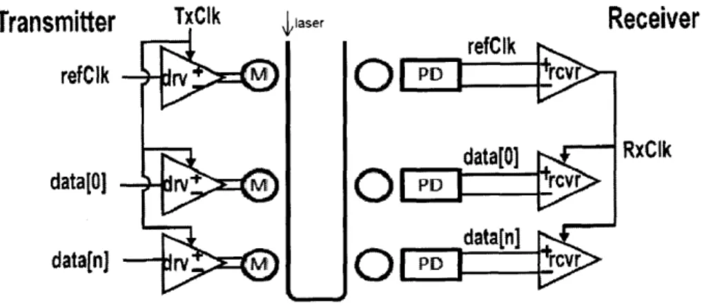
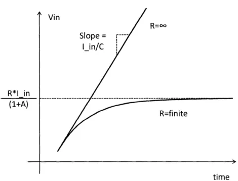
A 9GHz injection locked loop optical clock receiver in 32-nm CMOS
Texte intégral
Figure
Documents relatifs
We discuss the following three topics in turn: (1) the timing data contained in Table A2 ; (2) for both H1743 and XTE J1550−564, we show four selected correlation plots that relate
The afore mentioned frequency approach, called Vandermonde-subspace frequency division multiplexing (VFDM), projects the signal to the secondary receiver on the nullspace of the
From the Tm 3+ -doped GC absorption spectra, the percentage of active ions in the crystal phase was esti- mated: in the glass ceramic with the higher temperature treatment, it is
In this paper, we have investigated end-to-end link modeling and digital receiver design for a particular example of receiver ar- chitecture, for coherent 10 Gb/s BPSK
Then the lines of the CCD camera encode the depth of the sample and a A- scan is displayed without scanning along the image lines (since all the light incident on the
Abstract: This study under the title: "days of preference in the light of the Sunnah, the study contain tow chapter, the first one named meaning of preference inside this chapter
As Borsuk-Ulam theorem implies the Brouwer fixed point theorem we can say that the existence of a simple and envy-free fair division relies on the Borsuk-Ulam theorem.. This
[r]
