Advances in Non-Planar Electromagnetic Prototyping
by
Isaac M. Ehrenberg
B.A., Yeshiva University (2005)
S.M., Massachusetts Institute of Technology (2009)
Submitted to the Department of Mechanical Engineering
in partial fulfillment of the requirements for the degree of
Doctor of Philosophy in Mechanical Engineering
at the
MASSACHUSETTS INSTITUTE OF TECHNOLOGY
June 2013
@Isaac Ehrenberg, 2013.
TNh
r ba!by
grants to
MIT
permision to
reprOde
and
to
Mete ubldy papAer and eletronfc copies of this thesi3 docume
i who or in
parti any
medium
now known or
hereafter created.
/I
ARCHNES
ASSACHUSETINSTITUT-2I
R
E-l
1-r7
1/
Author...
...
Department of Mechanical Engineering
April 12, 2013
7?
'1 V V
Certified by ...
Sanjay E. Sarma
Fred Fort Flowers and Daniel Fort Flowers Professor of Mechanical
Engineering
Thesis Supervisor
A ccepted by ...
. ...
David E. Hardt
Chairman, Department Committee on Graduate Theses
Advances in Non-Planar Electromagnetic Prototyping
by
Isaac M. Ehrenberg
Submitted to the Department of Mechanical Engineering on April 12, 2013, in partial fulfillment of the
requirements for the degree of
Doctor of Philosophy in Mechanical Engineering
Abstract
The advent of metamaterials has introduced new ways to manipulate how electromagnetic waves reflect, refract and radiate in systems where the range of available material properties now includes negative permittivity, permeability, and refractive index. While analytical and numerical tools are equipped to analyze the complex configurations of materials and geom-etry that constitute many proposed devices, realizations have been limited in part due to fabrication. The fabrication processes used to construct the majority of metamaterial media are optimized to produce 2D products, including printed circuit board and microfabrication techniques, making the transition from two dimensional proof-of-concept to three dimen-sional prototype challenging.
In the last decade, several reports have documented the use of additive manufacturing to fabricate 3D electromagnetic devices, including gradient index lenses at both microwave and optical frequencies, and radio frequency lenses that attain resolution beyond the diffrac-tion limit. Though primarily used for facsimile display models, additive manufacturing is uniquely capable of addressing the needs of 3D electromagnetic designs which incorporate non-planar geometries and material inhomogeneity. The application of additive manufactur-ing to functional electromagnetic devices, however, is still uncommon, as the simultaneous layering of conductive and insulating materials remains complicated.
To further advance the start of the art, we report our application of additive manufactur-ing in conjunction with other fabrication tools to fabricate several electromagnetics devices. The first involved the design of an artificial magnetic conducting substrate to enhance UHF RFID tags in close proximity to metal surfaces, which normally detune antennas and destruc-tively interfere with any transmitted waves. The substrate incorporates 3D metamaterial unit cells, the fabrication and assembly of which were enabled by additive manufacturing. Additive manufacturing was then used to fabricate lightweight, self-supporting intercon-nected metamaterial structures. These structures exhibited minimal losses, making them ideal for a plano-concave microwave lens capable of focusing at 10GHz with the highest gain measured for a metamaterial lens to date. Other achievements include the fabrica-tion of frequency selective surfaces and antenna elements conformal to non-planar surfaces. Though many challenges remain to be overcome, it is clear that additive manufacturing has significant potential to contribute to the study and fabrication of electromagnetic elements.
Thesis Supervisor: Sanjay E. Sarma
Acknowledgments
It is with boundless appreciation that I acknowledge the many individuals that have aided, encouraged and inspired me to undertake and ultimately complete my graduate education in general and this thesis in particular.
Credit first goes to my Organic Chemistry teacher Prof. Bruce Hrnjez for suggesting that this Yeshiva boy apply to MIT, and Rosalyn Falk for ensuring the quality of that applica-tion. Upon acceptance, Lesley Regan and Joan Kravit both greeted me with warmth that has yet to dissipate despite the New England weather but which they periodically recharge regardless. It was they who directed me to Prof. Rohan Abeyaratne, whose door was always open during those overwhelming months before I joined Sanjay's lab.
After my initial conversation with Professor Sanjay E. Sarma, he told me to read two theses and call him in the morning. Two theses later, Sanjay's maniacal cunning and unwa-vering support continue to cultivate an atmosphere of camaraderie, education and innovation which I consider myself fortunate to have experienced. Despite his humble assertions to the contrary, neither thesis would have been possible without him.
Though one's own advisor has a vested interest in ensuring the success of his student's work, I am particularly grateful to Professors Timothy Gutowski and Nicholas Fang, who volunteered to serve as members of my thesis committee. They were generous with their time, complimentary of my research and always constructive with their criticisms.
In the end of the day, I owe much to the post-doctoral fellows, students and staff that populated the MIT Auto-ID Laboratory before and during my tenure as an MIT student, including Drs. Christian Floerkemeier, supervisor of my master's research, Stephen Ho, who among his other important duties diligently read a draft of this thesis, Ajay Deshpande, who is the only explanation of how I came to pass Dynamics, Sriram Krishnan, who answered the call on many occasions to assist my research and writing efforts in any way that he could, and Rahul Bhattacharyya, lab mate par excellence. Thanks also go to the ace Sumeet Kumar, for his help with the organization of this thesis, the magical powers of Dylan Erb, as well as Kat Donnelly, Austin Oehlerking, Justin Miller, Long Phan, Abraham Rosenfeld, and Erik Wilhelm, who all played a part, and Joshua Siegal, who coached me when it counted.
Despite spending a significant portion of my time at MIT on the second floor of Building
35, most of the heavy lifting that went into this thesis was done in the LMP machine shop
with the help of David Dow and Patrick McAtamney, in the Edgerton student shop run by the one and only Mark Belanger, and at the MIT Microsystems Technology Laboratories under the supervision of Eric Lim and Kurt Broderick. It was the energy, kindness and concern of these unique individuals that made getting my research done both possible and enjoyable.
Indispensable contributions were made to every chapter of this thesis by Dr. Bae-Ian Wu. I first met Dr. Wu in the spring of 2007 while taking 6.013 with our teacher Prof. Jin Au Kong, of blessed memory, and since then his patience, perfectionism and his insistence on making the second effort pushed me through to the end and beyond.
In addition to those above, I must acknowledge the Jewish communities at MIT, Harvard,
BU, Brookline, M.A. and the surrounding cities that provided me with the infrastructure
needed to function as an Orthodox Jew while in graduate school. Particular thanks are due to many friends near and far including the Barabans, Eleffs, Untermans, Zytos, Rabbi Levi
Altein, Erez Lieberman, Rabbi Gershon Segal, Jordan Whistler and many, many others.
My entire family has always been a source of inspiration and strength, from my
grand-mothers Bubby Genie and Bubby Sylvia, may they live and be well, to my nieces and nephews, with all my aunts, uncles, siblings and cousins in between. I hope and pray that our family continues to grow together.
My wife Rahel has displayed remarkable fortitude over the last few years as I struggled
to put together this thesis. While some credit for her resolve is attributable to the beautiful example set by her parents who prepared her so well for what to expect as the spouse of an MIT PhD student, I dedicate this thesis to Rahel in recognition of the uncountable frustrated hours for which it kept me distant from her, the faith she had in me that I would eventually prevail, and her desire for us to excel in all aspects of our lives.
Finally, I cannot begin to elaborate on the gratitude and appreciation I have towards my parents. I know it not for this thesis, nor this degree, for which they are most proud.
for Rahel,
Contents
1 Introduction
1.1 The Role of Geometry and Material Parameters in Electromagnetic Systems
1.1.1 Geom etry Control . . . . 1.1.2 Material Property Control . . . . 1.2 Material Parameter Control with Metamaterials . . . . 1.2.1 Challenges in Using Metamaterials . . . . 1.3 Thesis Contributions . . . . 1.4 T hesis outline . . . .
2 Metamaterial Electromagnetics and Fabrication
2.1 Derivation of Constitutive Parameters for Metamaterial Structures . 2.1.1 Analytic Approach . . . . 2.1.2 Parameter Extraction from Reflection and Transmission Data 2.2 Review of Metamaterial Fabrication . . . .
2.2.1 Common Fabrication Processes for Metamaterial Structures 2.2.2 Multilayer and Non-Planar Metamaterial Fabrication . . . . .
2.3 Additive Manufacturing for Complex 3D metamaterials . . . .
2.3.1 List of Additive Processes . . . .
2.3.2 Process Capabilities and Limitations . . . .
2.3.3 Additively Manufactured Metamaterials . . . .
2.3.4 Surface Modification of Additively Manufactured Structures .
2.3.5 Usage of Additive Manufacturing in this Thesis . . . . 2.4 Chapter Conclusions . . . . 23 . . . . 23 . . . . 24 . . . . 27 . . . . 30 . . . . 31 . . . . 34 . . . . 35 . . . . 36 . . . . 37 . . . . 38 39 . . . . 39 . . . . 40 13 14 15 16 18 20 21 22
3 Artificial Reflection in Depth 3.1 RFID Background ...
3.1.1 RFID Physics . . . . 3.2 The RFID Metal Problem . . . .
3.2.1 Possible Solutions to the Metal
3.2.2 The Ideal Solution . . . .
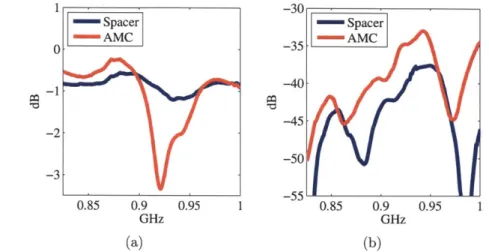
3.3 The AMC solution . . . .
3.3.1 AMC for UHF RFID . . . . . 3.3.2 Related Work . . . .
3.3.3 New Unit Cell Design . . . . .
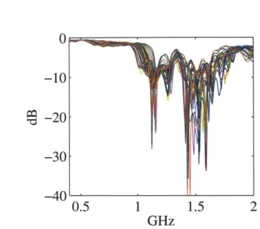
3.3.4 Initial Prototype Fabrication ai
3.3.5 Antenna Simulations . . . . .
3.3.6 Antenna Experiments . . . . .
3.3.7 Extension to RFID frequencies
3.3.8 Unit Cell Redesign...
3.4 Conclusions . . . . 3.4.1 AMC Implications . . . . 3.4.2 Fabrication Implications . . .
. . . .
Problem . . . . .. . . .
. . . .
. . . .
. . . .
. . . .
nd Characterization. . . .
. . . .
. . . .
. . . .
. . . .
4 Lost in Transmission4.1 Motivation for 3D Structures: Minimization of Loss 4.1.1 Self-Supporting Metamaterial Designs . . . .
4.2 S-Ring Metamaterial Unit Cell . . . . 4.2.1 Early S-ring Examples . . . . 4.2.2 Additively Manufactured S-Rings . . . .
4.2.3 Fabrication and Testing . . . .
4.3 S-Ring Metamaterial Lens . . . . 4.3.1 Negative Index Lenses . . . . 4.3.2 Related Metamaterial Lens Work . . . .
4.3.3 S-Ring Lens Design . . . .
41 . . . . 4 1 . . . . 4 2 44 44 47 48 50 51 52 53 56 57 59 60 67 68 68 69 70 70 71 72 72 73 75 76
77
794.3.4 Lens Fabrication . . . . 80
4.3.5 Single Layer Transmission . . . . 85
4.3.6 Copper Lens Evaluation . . . . 86
4.4 Conclusion . . . . 90
5 Conformable Coverage and Orthomorphic Radiance 91 5.1 Introduction . . . . 91
5.2 Conformal Masking . . . . 94
5.2.1 Other Masking Methods . . . . 94
5.2.2 A Non-Conformist Solution . . . . 95
5.3 Conformal FSS . . . . 96
5.3.1 FSS Applications . . . . 96
5.3.2 State of the Art FSS Fabrication . . . . 97
5.3.3 FSS Unit Cell Design . . . . 98
5.3.4 Conformal FSS Design . . . . 99
5.3.5 Conformal FSS Fabrication . . . . 101
5.3.6 FSS Evaluation . . . . 107
5.4 Conformal Antenna Array . . . . 108
5.4.1 Non-planar Substrate . . . . 109
5.4.2 Planar and Conformal Patch Antenna . . . . 110
5.4.3 Array Antenna Simulations . . . . 114
5.4.4 Fabrication . . . . 119
5.4.5 Antenna Array Testing . . . . 121
5.5 Conclusion. . . . . 122
6 Conclusion 125 6.1 Metamaterial Fabrication. . . . . 125
6.2 Summary of Contributions . . . . 126
6.3 Future Work . . . . 127
6.3.1 Thin AMC Manufacturing . . . . 127
6.3.3 Conformal Masking Process Development . . . . ... . . . . 128
6.3.4 Combining 3D and Non-Planar . . . . 129 6.3.5 Changing the Mindset . . . . 130
Chapter 1
Introduction
In this thesis, I study the fabrication of three-dimensional (3D) and conformal geometries and their affect on how electromagnetic waves reflect, refract and radiate. Recent innovations in areas such as communications, imaging, defense and security have generated significant interest in a wide array of 3D and conformal electromagnetic structures, sought after for their unique and often unnatural electromagnetic characteristics that are advantageous to both traditional and emerging applications [1, 2, 3].
I begin this introductory chapter by describing the components of a generic electromag-netic system, and how the behavior of electromagelectromag-netic waves in that system is a function of both geometry and material parameters. After giving examples of how electromagnetic de-vices incorporate both geometry and material parameters, I discuss the recent development of metamaterials, which have introduced a new level of control in electromagnetic system design. I then review several proposed metamaterial applications that have redefined the limits of conventional electromagnetics, but remain difficult to realize in practice partly due to complications associated with fabrication. This chapter concludes with a summary of the thesis contributions, and an outline for the remainder of the thesis.
Scattering
Radiation
Reflection
/
Transmission
n
Scattering
Figure 1-1: A generic electromagnetic system consisting of a radiation source and an object. When radiation emitted from the source is incident upon the object, it results in reflection, transmission, absorption and scattering.
1.1
The Role of Geometry and Material Parameters in
Electromagnetic Systems
The electromagnetic system sketched in Fig. 1-1 depicts an object illuminated by electro-magnetic waves emanating from a radiation source. When incident waves from the source encounter the object, the result is a combination of reflection, scattering, absorption and transmission. The nature of these phenomena is described by Maxwell's Equations
Vx E= -P
t
V - E = P (1.1) (1.2) (1.3)A
V -H = 0
(1.4)
where E and H are the electric and magnetic fields, J is the current density, p is the charge density, and e and y are the permittivity and permeability of the medium. When fully solved, Maxwell's Equations reveal the time changing electric and magnetic fields of the entire system. The inputs required to solve for all the unknowns in these equations are initial conditions of any source terms, boundary conditions and material parameters. Considering the scenario of Fig. 1-1, boundary conditions and material parameters refer to the overall geometry and constituent materials that make up the radiant antenna, the incident upon object, and the background environment. The geometry and material makeup of these three elements afford an avenue to influence electromagnetic fields, and design an electromagnetic system to produce specific outcomes. While any outcome is the result of many intertwined physical factors, in the following sections we will highlight several examples of how geometry and material parameters individually can provide control over different aspects of an electromagnetic system.
1.1.1
Geometry Control
Radiation from Antennas
The crucial role played by geometry in the design of radiative system components is apparent from the fact that many antenna properties are dependent on geometry, resulting in different antenna types for different applications. Towering mast antennas are used to broadcast long wavelength signals for AM or FM radio stations, while arrays of smaller patch antennas optimized for transmitting and receiving at much shorter wavelengths sit atop cell phone towers. Aside from operation frequency, physical dimensions are also important for key antenna performance parameters such as bandwidth and gain, and the overall radiation pattern.
Reflection off Reflectors
While control over antenna geometry can go a long way towards building a functional system, propagating electromagnetic waves often require redirection, which can be achieved through the proper design of reflectors. Reflectors are surfaces shaped to reflect incident waves in a particular way. A common example is a parabolic reflector dish, which are used in many applications such as radio astronomy and sattilite television. These same curved dishes can also be used to redirect and collimate, or spread out, the signals of radiation sources.
Transmission Through Lenses
When reflection is impractical, transmissive devices can be used to redirect electromagnetic waves. Transparent objects with properly configured surface curvatures, referred to as lenses, can focus or spread incident radiation. Tight control over surface geometry allows focal lengths to be optimized for purposes such as imaging or tumor ablation. One example of such a lens is the human eye, which constantly refocuses on objects near and far as muscles
alter the shape of its lens.
Scattering for Stealth
Scattering is often an undesired byproduct in systems designed to reflect or transmit, with the misdirection of waves caused by imperfections in surface geometry. Though care is taken during the fabrication process for many applications to reduce surface roughness and limit scattering, other applications such as stealth technology rely on increased scattering and reduced reflection. By scattering most of the energy away from a mono-static radar station, the radar cross section of an object can be significantly reduced to help avoid detection.
1.1.2
Material Property Control
While the previous section focused on the relationship between function and geometry, ma-terials and their properties also play a crucial role in electromagnetic system design. The
" Permittivity (e), which includes the electrical properties of free space and the ratio
of the electric dipole moment per unit volume of the material. The electric dipole moment can be permanent, or induced by the migration of electric charges [4].
" Permeability (p), which includes the magnetic properties of free space, and the
per-manent or induced magnetic moments within the material.
Permittivity and permeability together describe how electromagnetic waves interact with materials, including the velocity v at which waves travel through material,
v = (1.5)
where c is the speed of light in vacuum, the wavelength A with which they travel
A = c(1.6)
where
w
is the angular frequency, how quickly energy is absorbed within a material, and wave behavior at the interface of two different materials. All these material effects and their consequences need to be considered when designing an electromagnetic system.Material Effects on Radiation
While many antennas consist of metallic radiative elements, materials surrounding those elements can have a significant impact on antenna parameters. For example, a substrate with a high dielectric constant can lower the resonance frequency and bandwidth of a patch antenna. Dielectrics are also used as radiating elements themselves, especially at higher frequencies where metals radiate less efficiently.
Dielectric Reflection
The precise arrangement of materials with different properties can be used to build reflective elements. By properly layering materials of higher and lower dielectric constants, waves incident on a material boundary above the critical angle can be forced to undergo total
internal reflection. This effect is useful for the guiding of waves in fiber optic cables, or the
construction of highly reflective dielectric mirrors and quarter wave elements.
Transmission through Dielectrics
Material parameters are also important for the design of transmissive devices. Lens proper-ties such as focal length are dependent on the material's refractive index in addition to the lens surface curvature. Lenses made from higher refractive index material have shorter focal lengths than lenses with lower indices.
Reduced Scattering with (Lossy) Materials
Aside from geometric considerations, scattering can be controlled and reduced through the incorporation of radar absorbent materials. These materials often have permeabilities that feature a significant imaginary part. In the process of absorbing the incident radiation, re-flection and transmission are also reduced, which can be useful for stealth or electromagnetic noise cancellation purposes.
1.2
Material Parameter Control with Metamaterials
The recent development of electromagnetic metamaterials has provided additional freedom to electromagnetic system designers by extending the range of available material parame-ters. Natural and synthetic bulk materials only provide a limited range of permittivity and permeability values, mostly concentrated in the top right quadrant of Fig. 1-2. In contrast, metamaterials have shown extreme or unique electrical properties not previously observed in natural materials [5]. To generate these unnatural material properties, metamaterials in-corporate heterogeneous mixtures of different materials, often in intricate predetermined ge-ometric patterns. These constructs interact with incident electromagnetic waves and change the response of the composite material to something different than the constituent bulk materials. By purposefully designing the size, shape, periodicity and material of any in-clusions, researchers have introduced new ways of controlling how electromagnetic waves radiate, reflect, transmit and scatter.
Ii
ALPlasma
Medium
UDouble
Negative
Metamaterial
Most
Materials
Magnetic
Plasma
Figure 1-2: The range of electromagnetic parameters, with most materials belonging to the upper right hand quadrant, and double negative metamaterials existing in the bottom left hand quadrant.
Altering Radiation with Metamaterials
Several studies show how metamaterials can be used to affect antenna properties [6, 7, 8, 9].
In one example, a spherical shell structure was designed to alter the radiation pattern of an antenna so that it mimics the pattern of an antenna with a larger aperture [10]. The proposed method applied to generate this aperture transformation also provides a methodology for designing antennas with arbitrarily high levels of directivity.
Artificial Reflection Surfaces with Metamaterials
Metamaterials have been used to alter the properties of reflective surfaces [11, 12]. Normally, metal surfaces reflect electromagnetic waves with an added phase of 1800. However, by covering the surface with a thin layer of metamaterial, the phase accrued by the reflected waves can be precisely controlled. This allows for the design of reflectors without large curvatures, and other substrates that are beneficial for near metal antenna designs [13, 14].
Enhanced Transmission with Metamaterials
Lenses made from regular materials are useful for focusing and imaging but their resolution is capped by the diffraction limit, which sets the minimum spot size for imaging through a lens
[15].
Lenses made from metamaterials, however, are not subject to the same diffraction limit [16]. Several studies have confirmed that lenses made from slabs of metamaterial with a refractive index of n = -1 are capable of imaging point sources with sub-diffraction limitedresolution, or super-resolution [17, 18].
Reduced Scattering with Metamaterials
Metamaterials can also be used to completely eliminate unwanted reflections and scattering. Other scattering reduction methods which redirect or absorb incident waves are only capable of evading detection by mono-static radar systems, where the source of the radar signal is also the detector. In the mono-static case, as long as reflected or scattered waves don't return to the radar antenna, the stealth object remains undetected. These methods fail in the case of bi-static detection systems, which act like trip-wires by detecting changes or interruptions to transmitted signals. To avoid detection in this scenario, a metamaterial shell can be designed to surround an object and redirect all the incident radiation so that the signal can be transmitted without any scattering. Metamaterials designed for this purpose are called invisibility cloaks, as they render a would-be scatter invisible to incoming radiation [19, 20].
1.2.1
Challenges in Using Metamaterials
Though metamaterials have been a topic of great interest to the electromagnetics community for over a decade, there remain significant issues that need to be overcome before metamate-rials can realize their potential to greatly enhance electromagnetic systems and enable new devices.
e Loss: Many metamaterials suffer from significant losses that preclude their use in
prac-tical devices. One source is ohmic loss, or energy dissipated as a result of current flow through materials with a finite conductivity. Ohmic loss is particularly problematic in metamaterials that contain metallic inclusions and are active around resonances
which generate high currents and field levels. Non-conductive dielectrics are a second source of loss, causing impedance mismatches that result in unwanted reflections, and propagation losses as transmitted waves propagate through the material [21].
e Bandwidth: For any particular design and prototype, metamaterial properties are only
observed over a finite frequency band. This is typical of the resonance phenomenon inherent to many designs, where the resonance frequency and quality factor are highly dependent on the physical dimensions of metamaterial inclusions. Bandwidth is also limited by the frequency response of the constituent materials used to fabricate the metamaterial [22, 23].
o Fabrication: Metamaterials fabrication is challenging because it requires complex pat-terns involving at least two materials with different properties. The task of creating such patterns lends itself to layered manufacturing processes. Layered processes, which are usually combinations of selective 2D additions and subtractions of material using combinations of patterns, binders, resists and enchants, have understandably been the most common approaches to metamaterial fabrication in the literature. While
2D metamaterials have been successfully fabricated and used to demonstrate
interest-ing phenomena, many metamaterial designs and applications such as those mentioned above require non-planar and 3D geometries, which can be difficult to achieve with standard 2D fabrication techniques.
1.3
Thesis Contributions
In this thesis, I propose both new 3D designs and the use of alternative fabrication methods to overcome some of the challenges and limitations imposed by conventional methodologies on the fabrication of metamaterials. My specific contributions are:
* The fabrication of a new 3D metamaterial unit cell for use with planar dipole RFID tag antennas.
e The fabrication of a lightweight, self-supporting plano-concave 3D metamaterial lens
" Proposal of a new methodology called "Conformal Masking" for conformal electromag-netic fabrication on curvilinear surfaces.
" The fabrication of a conformal frequency selective surface using a conformal mask.
" The fabrication of a conformal patch antenna array using a conformal mask.
1.4
Thesis outline
The remainder of this thesis is organized as follows. Chapter 2 gives a brief tutorial on the electromagnetics of metamaterials and overview of the techniques used to fabricate 2D and
3D metamaterials, with a focus on additive manufacturing techniques which are utilized in
subsequent chapters. In chapter 3, as a motivation for the study of metamaterial reflection enhancement, I present a brief discussion of the problems encountered when operating RFID tags in close proximity to metal surfaces. That is followed by an analysis of a potential metamaterial solution the the RFID metal problem, and the proposal of a 3D metamaterial design and its fabrication. In chapter 4, I present an overview of the challenges faced by transmission based metamaterial designs, followed by the fabrication and implementation of a self-supporting lightweight plano-concave lens built from 3D metamaterial unit cells. In light of the fabrication insights garnered from the previous chapters, chapter 5 introduces a new method for the fabrication of conformal electromagnetic structures. This method is then used for the fabrication of a conformal frequency selective surface (FSS) and conformal patch antenna array. I conclude with a review of the thesis contributions, and future directions for this work in Chapter 6.
Chapter 2
Metamaterial Electromagnetics and
Fabrication
To place the design and fabrication of metamaterials and other electromagnetic structures in context, I begin this chapter with a brief tutorial on the electromagnetics of metamaterials. Using the example a split-ring resonator, I derive relative material parameters from both an analytic and simulation perspective.
Following the tutorial is a review of common manufacturing methods utilized to fabri-cate metamaterial structures. I then discuss the use of additive manufacturing processes as a means of prototyping complex 3D metamaterials structures and other electromagnetic devices. Though the primary focus of these additive techniques in the past has been me-chanical design, in this thesis I leverage the flexibility afforded by such processes to further the boundaries of electromagnetic device design and fabrication.
2.1
Derivation of Constitutive Parameters for
Meta-material Structures
Maxwell's Equations as presented in Section 1.1 are the fundamental laws governing elec-tromagnetic fields in both free space and within materials. The material parameters f and y that appear in those equations are abstractions that encapsulate the effect of matter on
electromagnetic fields or propagating waves relative to the electric and magnetic effects of free space, which are universal physical constants represented by t0 and po.
In the case of bulk materials, the contributing factors to c and y are sub-atomic, atomic and molecular structures. For metamterials, the contributing factors to e and y are instead the result of properly designed and oriented mixtures of bulk materials. In some situations, it is possible to analytically derive c and p of metamaterials from first principles. When analyt-ical methods are not available, c and yt maybe be extracted from relative measurements or simulations. In the following two sections, the effective permeability of a split ring resonator will be derived according to both of these approaches [24, 4].
2.1.1
Analytic Approach
Consider an infinitely periodic 2D array of split ring resonator cells, where at the center of each unit cell rests a split ring of radius R (Fig. 2-1). The unit cells are square and have a dimension of 1. The fractional area encompassed by the ring is
f
= R2, and the free spacein and around the ring is characterized by co and po.
Let Ho be a time-harmonic magnetic field. Without the existence of any split rings, the application of Ho would result in an unperturbed magnetic field throughout the cell. However, when applied in the presence of the split rings, Ho induces a surface current J, along the ring, and a strong electric field E2 between the gaps oriented in the direction of the current flow. According to the boundary conditions imposed by Maxwell's Equations, the induced current J, is the difference between the external magnetic field and magnetic
E2
El Ide
d
Hint He xt
tedi
field inside to the ring radius
Js = Hext - Hint
(2.1)
The split ring causes an inhomogeneity which complicates the magnetic field within the cell. To simplify the characterization of the magnetic field, we use a homogenization law and utilize an effective bulk permeability peff to average the external and internal fields over the area of the cell [25, 24],
LeffHext =
fHin
+ (1 - f)Hext. (2.2)We can thus define the effective permeability as
_
fHint
+ (1 - f)Hext _ Hext -f
Jsf
Jp
-f-
= 1
s +-(2.3)
e Hext Hext JS + Hint
To relate J, directly to Hint, we apply Faraday's law, this time in the integral form,
E - di= -
oH
. dS (2.4)where the contour C is the ring's circumference enclosing the area S when d is infinitely small. Assuming the ring is made of perfect conductor such that there is no electric field within the ring structure itself and E1 = 0, the only contributions to the right side of Eq. 2.4
come from the fields within the gaps,
J E - dI= -2dE 2 (2.5)
corresponding to the voltage accumulated when following the closed contour. Assuming Hint is uniform within the ring, the right side of Eq. 2.4 becomes
which results in
- 2dE2 = iwIo7rR2Hit (2.7)
relating E2 to
Hist.
We then apply boundary conditions along the ring gap, which relates the charge density along the ring edge fc to a difference in the divergence field D normal to the edge of the ring, we get
n
-(D
1 - D2) = Ps(2.8)
where p, is the charge per unit length. Since there is no field within the ring, the equation becomes
D = ps. (2.9)
Multiplying both sides by le and taking the time derivative of this time-harmonic system
where d - i, we get
dt dt
If we now let L = pto7rR2 and C = col/2d and plug them into Ipteff the result is
Peff =[ 1 - = [1 - 2 2 (1
where w = 1 After choosing physical parameters (1 = 2.024 mm,R = 1 mm,lc = 0.875 mm
and dc = .01mm), we can plot Eq. 2.11, and observe that this configuration features an effective permeability that is negative in the frequency range wo <2 < WO/(1 - f)(Fig. 2-2).
30- 20- 10-S-10 ' -20- -30- -40--50 1 2 3 4 5 6 7
GHz
Figure 2-2: The relative permeability of the split ring configuration, which is negative in the post resonance region just above 4 GHz, as calculated using Eq. 2.11.
2.1.2
Parameter Extraction from Reflection and Transmission Data
In addition to analytical derivations, experiments and simulations are also useful for analyz-ing metamaterial structures. Data from experiments or simulations can be used to observe metamaterial behavior and verify analytical models such as the one in the previous section, or provide an initial estimate of the relative parameters when an analytical model is not
available.
We will now review the procedure for extracting the unknown relative permittivity and permeability of a periodic metamaterial structure. Consider a plane wave normally incident upon a medium (Fig. 2-3), which consists of three regions. Region 1 and Region 3 are both free space, represented by tO and po. Region 2 is a metamaterial featuring unknown ( and
y, but it has a known thickness d. When the plane wave encounters the boundary between Regions 1 and 2, it results in both reflection R and transmission T determined by
1 - 1k2
R = 2k1 (2.12)
1 - 1k2
R + T = 11
where the wavenumber k,2 = wlynen within each region.
While the reflected wave no longer encounters any media other than free space, the transmitted wave continues until it reaches the boundary of Regions 2 and 3. What is transmitted at this juncture continues to propagate through Region 3, but the reflected component redirects back towards the boundary of Regions 2 and 1, and the process repeats. The sum of all the reflection and transmission terms is:
Ro
01+
R12e 2 k~cdRtotal
= 1 +
tft2kd(2.14)
1
+
Ro1R12e
i2k2dTo1T1
2eik2d
Ttotal =
+oiT1 2ek2d (2.15)1
+
Ro1R12e
r2k2d'
where Rab and Tab represent the reflection and transmission coefficients at that boundary of Regions a and b. If Rtotai and Ttotal are known from a simulation or experiment, then we can use these equations to extract the unknown e and y from Region 2.
As an example, a simulation of the split ring with the same parameters as before was performed using Ansoft HFSS, a commercially available FEM solver for electromagnetic
Region 1
Region 2
Region 3
E01 P0 E, I E01 Y0
Eoe ikx
Ttotal
Rtotai
d
Figure 2-3: A plane wave is incident upon a layered medium, the middle of which contains a split ring array and is of unknown permeability and permittivity. The unknown parameters can be extracted if the total reflection and transmission through the medium is known by way of experiment or simulation.
3 4 5 6 1 2 3 4
GHz
GHz
(a) (b) 6 -20'. W-1 2 3 4 5 6GHz
(c)Figure 2-4: (a) The S-parameter output from a split ring simulation which was used to retrieve the relative (c) permittivity and (b) permeability of the split ring medium.
systems. The split ring was oriented along the y-axis and illuminated by a plane wave propagating along the x-axis. Periodic boundary conditions were applied along the y-axis and z-axis to simulate the affects of an array configuration. Reflection and transmission are reported as Su1 and S21, from which the relative permeability and permittivity can be
2.2
Review of Metamaterial Fabrication
While theory and simulation are valuable tools for the design and analysis of metamaterial structures, the ultimate goal is validation through experiments, followed by application in an actual device. To that end, the fabrication of materials with engineered electrical properties began in the early 2 0th century, when metallic inclusions were arrayed within dielectric slabs
for the purpose of creating high dielectric constant materials with relatively low densities. Though research on artificial media continued in subsequent decades, interest in metamate-rials surged after the prediction and demonstration of negative refraction with arrays of wire and split ring resonators printed on circuit board substrates [26, 25, 27]. Initially operating only at microwave frequencies, it took less than a decade for structures to be fabricated that displayed metamaterial properties into the optical spectrum [28].
The rapid evolution of metamaterials from microwave to optical frequencies was due in part to the availability of robust manufacturing techniques previously developed for the electronics and microfabrication industries. Like other devices such as circuit boards or in-tegrated chips that operate according to electromagnetic principles, the ordered placement of distinct materials is often required for metamaterials to function. In the case of a printed circuit or a micro-electromechanical device, specific patterns of conductors and insulators are needed to complete circuits and allow current flow. Metamaterials likewise require the ordered placement of materials to create the desired electric or magnetic response. By the time metamaterials were rediscovered at the start of the 21rst century, semiconductor fab-rication methods were already advanced and capable of 100 nm linewidths. This allowed metamaterial geometries resonant at GHz to be scaled with high precision to the small di-mensions required for metamaterials to be active at much higher frequencies.
The fabrication of the many metamaterials that have been showcased in the literature often involves a combination of additive and subtractive processes. The choice of available processes for any particular design is dictated both by the frequency range of interest and dimensionality on the level of each individual metamaterial element and the entire device as a whole [11, 27, 29]. The following section contains a list of processes commonly used for the fabrication of 2D metamaterial structures. That is followed by a discussion of 3D
metamaterial fabrication.
2.2.1
Common Fabrication Processes for Metamaterial Structures
Many metamaterial structures are made with PCB or micro-fabrication techniques. Though process details and tools vary for these two manufacturing systems operating at different length scales, PCB and microfabrication methods are similar in their purpose, which is patterning surfaces with structures. Both begin with a substrate material, and use various additive and subtractive processes to alter the the substrate surface. For PCB processes, the substrate is often a polymer such as FR4, polyimide or PET. Microfabrication substrates are commonly silicon, silicon carbide or glass. Some of the processes used to modify those substrate surfaces are:
e Lamination: Used to add layers of copper or other materials through the application
of pressure and heat, and often with the aid of adhesives.
e Silk Screen Printing: A process used in PCB production to apply an etch mask
di-rectly to a substrate surface through a patterned screen. Once the pattern is applied, substrates are placed in a chemical bath to etch exposed copper metal, leaving only the desired pattern.
e Micromilling: A subtractive process that removes material by cutting with a small
milling machine at high spindle speeds. This mechanical process is used in PCB fabri-cation to form via holes within PCB substrates. It is also useful for other metamaterial designs that require holes. The smallest diameter holes available from commercially produced PCB bards are on the order of 0.1 mm, though end mills with smaller diam-eters do exist.
e Laser Ablation: A process that uses a laser to remove material. It can be used to
pattern a surface or form via holes in films and substrates.
e Direct Write Technology: The use of a stylus to draw lines on a substrate with
" Electroplating: A electrochemical process used to deposit metals on conductive
sur-faces. Plating is useful for the deposition of relatively thick layers of material, such as the filling of via holes in PCBs.
" Sputtering: A thin film deposition process where a target material is bombarded with high energy ions from a nearby plasma. The plasma particles collide with the target at very high speeds, knocking off small particles from the target material, which then deposit on a substrate below. This process takes place in a low pressure environment to ensure the mean free path of the sputtered particles is sufficiently long so they reach the substrate before reacting with other particles in the local atmosphere. The thickness of deposition is often limited by internal stresses within the sputtered material, which can overwhelm adhesive forces between the film and substrate.
" Physical Vapor Deposition: Another thin film deposition process in which a material is heated in a vacuum to the point where it begins to evaporate and particles precipitate on to the substrate surface. For metals, the heat can be generated resistively, while dielectrics often require bombardment with high energy electrons.
" Photolithography: A process in which a light sensitive polymer layer is used to pattern an underlying thin film. This process is commonly used for both PCB and microscale production, capable of linewidths ranging from many microns to nanometers, depend-ing on the exposure system used. It usually involves several process steps:
- Spin coating: A process in which liquid photopolymer droplets are placed onto a substrate that is rotating with high angular velocity. While centrifugal forces spread the droplets, a uniformly thin layer remains on the substrate surface due to contact forces.
- Development: A process where a photopolymer is selectively exposed to radiation through a photomask, a transparent film with a darkened pattern printed on its surface. The mask is either placed directly above the surface to be patterned, or imaged through a lens system.
solution, leaving an etch resistant pattern atop the underlying thin film. The exposed thin film is removed in a similar fashion, with only the patterned area
remaining.
* Lift Off: A process where thin films are deposited on substrates that are pre-patterned with a layer of sacrificial material. After the thin film deposition, which must be thin enough to leave some sacrificial material exposed, the sacrificial material is removed
by etching, leaving only the thin film pattern on the substrate surface.
" Electron Beam Lithography: A process similar to to photolithography where only high
energy electrons are used to develop resist masks, as opposed to UV or other electro-magnetic radiation. The small wavelength of the electrons provides this lithography process resolution on the order of 10 nm, which is useful for the fabrication of meta-materials structures active at THz frequencies.
" Interference Lithography: Another process similar to photolithorgraphy where the
pat-tern that results on the substrate is an interference patpat-tern created by the diffraction of light through a grating, as opposed to a pattern printed onto a photomask. This process is able to produce periodic patterns with very high resolution.
" Nanoimprint Lithography: A patterning process in which a mold is used to
mechani-cally deform a resist or thin film. As a mechanical process, smaller features are possible relative to optical systems which are limited by diffraction.
" Focused Ion Beam Milling (FIB): A subtractive process which uses a focused beam
of high energy ions to remove material from a substrate surface. The ions bombard the film clad surface, causing the ejection of film or substrate particles. This method is used to pattern films with nanometer resolution, and has a shorter cycle time than other electron beam lithography processes.
" Shadow Masking: A process that allows for the direct deposition of patterned thin
films by masking the substrate with a monolithic stencil. As an alternative to photo-lithography, it removes the many process steps involved with chemical etching, but is unable to produce the same quality line widths.
Figure 2-5: A multi-layer stack of split ring resonators, fabricated using electron beam lithography, anisotropic etching and planarization steps [30].
2.2.2
Multilayer and Non-Planar Metamaterial Fabrication
The fabrication of 3D metamaterial structures can be significantly more complicated than
2D structures. Construction of a 2D pattern is simplified by the fact that any point within a 2D plane is always accessible via the remaining spatial dimension. This is not the case for 3D
metamaterials, which often consist of stacked 2D layers. Such stacks have been fabricated utilizing processes that incorporate multi-layer PCBs, chemical-mechanical planarization, liftoff and deep anisotropic etching.
The multi-layered fabrication of planar structures is limited because it can be difficult to produce metamaterials sensitive to incident fields polarized along multiple directions. For example, the stack of split rings in Fig. 2-5 only has a magnetic response for radiation incident from within the plane of the image with its magnetic field polarization parallel to the loop normal. The split ring arrangement in Fig. 2-6, which has an isotropic magnetic response, would be very difficult to fabricate using multilayer methods. To achieve the multi directional response, individual layers of planar structures have to be manually assembled
and weaved together or manually assembled into the proper arrangement.
Another consideration that affects the viability of multilayer metamaterials is dissipation loss. Many metamaterials have significant losses with only a single layer of material, as
Figure 2-6: A cubic unit cell with split ring oriented in three different directions to create an isotropic response [25].
incident electromagnetic waves propagate through lossy dielectrics and induced currents traverse along the surface of imperfect electric conductors. The inclusion of additional layers compounds the problem, further reducing metamaterial efficiency.
2.3
Additive Manufacturing for Complex 3D
metama-terials
In this thesis, I consider additive manufacturing as an alternative method to produce 3D metamaterials. Additive manufacturing techniques have been developed over the last quar-ter century to enable the rapid prototyping of mechanical components and tooling. Before additive manufacturing, the fabrication of prototypes often involved a significant investment involving multiple tools and machines and extended waiting periods. Today, rapid prototyp-ing techniques can build a newly designed mechanical structure in a matter of hours.
All additive manufacturing processes build parts in layers. While similar to the
techniques used for additive manufacturing are carefully selected for their ability to form monolithic, self-supporting structures.
2.3.1
List of Additive Processes
Some of the more commonly used additive processes for rapid prototyping include [31]:
" Stereolithography (STL): A process in which a vat of photocurable liquid polymer
is selectively cured by a UV laser source. The laser is focused on select points in the x-y plane, photopolymerizing the material at those locations. The first hardened layer of the part, which rests on movable platform, is then lowered into the vat to allow the next layer to be added on top. If previous cured material is unable to support subsequent layers, perforated support structures can be formed from the liquid polymer, and removed in a finishing step.
" Fused Deposition Modeling (FDM): A process where parts are produced from stacked
layers of thin extruded plastic rods. As each layer of heated plastic is extruded, it partially melts the plastic below, allowing the two layers to bond upon cooling. A support material separate from the model material can also be extruded when required, which is removed upon part completion.
* Selective Laser Sintering (SLS): A process by which a powder is selectively sintered to form an single object. Similar to STL, a laser is used to sinter specified regions in a layer of powder. After each layer is solidified in the desired locations, a new layer of powder is flattened over the previous layers. Unsintered powder is used as the support material. This process is capable producing ceramic, metallic and polymer parts.
" Three-Dimensional Printing (3DP): A process similar to SLS which instead uses
adhe-sive binders to form parts from layers of powder. After being printed, the green parts can be sintered to fuse the powder.
The precision of most of the process in the above list range from .015 GHz to 1 GHz. Similar processes have been developed for micro and nano structures, such as Micro-Stereolithography
2.3.2
Process Capabilities and Limitations
Additive manufacturing is a geometrically flexible process capable of producing shapes, sur-faces and assemblies that are difficult to produce with conventional automated fabrication equipment. The price for that flexibility comes at the expense of the price per part, but also limited material selection, dimensional accuracy and weakened structural properties. In situations where the tolerances are not overly strict such as parts meant for display purposes, these limitations may not be significant. These capabilities and limitations are most relevant when these processes are used to fabricate functional devices. The following will enumerate how the capabilities and limitations of additive manufacturing relate the requirements for electromagnetic and metamaterial devices:
e Geometric flexibility afforded by additive manufacturing is a capability that could
be of great value to electromagnetic designs. As discussed in Section 1.1.1, all parts of an electromagnetic system are influenced by geometry. The availability of additive manufacturing for electromagnetics results in a widening of the geometric design space.
* Material availability in additive manufacturing has significant implications for the
func-tion of electromagnetic devices that can be fabricated. While processes are capable of building parts from either dielectrics or metals, most cannot incorporate these comple-mentary materials into a single construct due to the incompatible process requirements. This is especially relevant for the fabrication of metamaterials, which may require the strategic placement of both conductors and dielectrics. Many processes do support parts built from two different but materials, which can be useful for the introduction of electrical property gradients.
e Dimensional accuracy of structures is relevant for designs with critical dimensions, such
as narrow band resonant structures, and other frequency dependent geometries.
e Weakened material properties are relevant for electromagnetic design, both from the
standpoint of limits resulting from structural instability, and how those may be related to adverse affects on electrical properties, such as the reduced conductivity of selectively sintered metal parts relative to parts machined from a bulk slab of conductive material.
2.3.3
Additively Manufactured Metamaterials
Despite the limitations, there remains a large window of opportunity for the application of additive manufacturing to electromagnetic design. The following are three examples of metamaterials fabricated additively:
e Gradient Refractive Index Lens: Sachs and Wang employed slurry based 3DP for the
fabrication of gradient index lenses [32]. The printed lenses were built from aluminum nitrate or barium acetate doped silicon dioxide power. The concentration of the dopant was varied at each point to give the lens its refractive index profile. After printing, the lens went through a heat treatment and sintering procedure, fusing the powder together and transforming the dopant into an oxide. Many aspects of the fabrication process were difficult to control, such as the migration of dopant during sintering which distorted the intended gradient index profile, highlighting the considerations that must be taken to properly incorporate multiple materials in 3D printing or similar additive processes.
e Luneberg Antenna: Liang [33] used a layered photo-polymerization process to fabricate
a 3D X-band Luneburg lens antenna, a gradient index structure designed to focus radiation on its outer surface. Instead of using a material dopant to define a gradient index, voids of various sizes were arranged within the printed volume. These voids effectively created a mixture of polymer and free space, the refractive index of which was proportional to the volume of polymer versus free space in any given voxel.
e 3D Split Ring Array: One example can be found in the literature that mentions rapid
prototyping of metamaterial blocks including both metallic and dielectric materials. Though few details are given, Mercure [34] discusses the fabrication of a Negative Index material that incorporates both a cubic intersecting grid of metallic wires and an array of metallic helical inclusions. As the helical inclusions are not electrically connected to one another, a dielectric support material is incorporated as a background material.
2.3.4
Surface Modification of Additively Manufactured Structures
While the final example of the previous subsection discusses the fabrication of arrayed metal-lic elements supported within a dielectric matrix, in today's additive manufacturing market one would be hardpressed find a commercially available machine capable of producing parts that contain both metals and dielectrics. Until that option becomes more widely available, post-process surface modification represents a viable means for overcoming some of the ma-terial limitations associated with additive manufacturing. An example of this is presented
by Rudolph [18, 35] in the fabrication of an isotropic 3D NRI metamaterial. Each
metama-terial unit cell consisted of a 3D cubic frame fabricated via STL. The surface of the polymer frame was then partially metalized with an electroless plating process, after which 12 surface mount capacitors were soldered at the middle of each leg.
2.3.5
Usage of Additive Manufacturing in this Thesis
Additive manufacturing and surface modification techniques were utilized in this thesis for the fabrication of 3D metamaterials and conformal electromagnetic structures:
e In Chapter 3, both a base material for metamaterial unit cells and a scaffold to aid in
cell arrangement were produced using FDM and layered photo-polymerization. Surface modification included the addition of copper and polyamide tape for the fabrication of an Artificial Magnetic Conductor substrate.
e In Chapter 4, hundreds of interconnected 3D S-ring structures were fabricated using
layered photo-polymerization. The surface was modified with the addition of a metallic layer through a PVD and sputtering processes.
e In Chapter 5, the surfaces of non-planar structures fabricated with layered
photo-polymerization were selectively coated with the aid of shadow masks also fabricated with layered photo-polymerization, in a process I have called Conformal Masking.
2.4
Chapter Conclusions
In this chapter, I reviewed the basic electromagnetics of metamaterials and common methods of fabrication. Through the derivation of the split ring resonator's effective permeability, I showed how the introduction of metallic inclusions can be used to change a material's prop-erties. The analysis also provides a clear connection between the geometry of the inclusion, and the frequency dependent nature of the inclusion's effect. While theoretical analysis is not always possible, extraction of parameters via simulation is another viable route, allowing for the study of complicated structural designs.
Though the virtual design space for metamaterials is bounded only by computational resources and Maxwell's Equations, the fabrication space is much more limited. Limitation exists because metamaterials require the ordered mixing of two or more bulk materials, and these materials must be compatible, in that they can be processed side by side in a con-trollable way. This fabrication challenge is hard, but its one that has been met before by the PCB and microfabrication industries, utilizing the processes listed in this chapter to fabricate metamaterial prototypes.
I also introduced additive manufacturing techniques, which have recently been used in the fabrication of electromagnetic devices, and will be utilized for the fabrication of devices

![Figure 2-5: A multi-layer stack of split ring resonators, fabricated using electron beam lithography, anisotropic etching and planarization steps [30].](https://thumb-eu.123doks.com/thumbv2/123doknet/13886909.447148/34.918.281.616.132.428/figure-resonators-fabricated-electron-lithography-anisotropic-etching-planarization.webp)
![Figure 2-6: A cubic unit cell with split ring oriented in three different directions to create an isotropic response [25].](https://thumb-eu.123doks.com/thumbv2/123doknet/13886909.447148/35.918.272.608.135.470/figure-cubic-oriented-different-directions-create-isotropic-response.webp)