Advanced Techniques for Fast Offset
Cancellation Limit Amplifiers
by
Carsten F. Jensen
MASSACHUSETTr, INSTIUT] OF TECHNOLOf o'NOV 13 2008
LIBRARIES
S.B. In Electrical Sciences and Engineering
MIT, 2006
Submitted to the Department of Electrical Engineering and Computer Science
in Partial Fulfillment of the Requirements for the Degree of
Master of Engineering in Electrical Engineering and Computer Science
at the Massachusetts Institute of Technology
August 2007
©2007 Massachusetts Institute of Technology All Rights Reserved
Author
Department of Electrical Engineering and Computer Science August 2, 2007
Certified by
Michael H. Perrott
As ociate Pro of Electrical Engineering
-7-fW Tosis Supervisor
Accepted by
Arthur C. Smith Professor of Electrical Engineering Chairman, Department Committee on Graduate Theses
Advanced Techniques for Fast Offset
Cancellation Limit Amplifiers
by
Carsten F. Jensen
Submitted to the Department of
Electrical Engineering and Computer Science
on August 2, 2007 in Partial Fulfillment of the Requirements for the Degree of Master of Engineering in
Electrical Engineering and Computer Science
ABSTRACT
As the need for higher data rates to end users increases, new technologies are required. Passive optical networks promise a vast improvement over previous methods, but they require amplifiers which can quickly adapt to changing input power levels. This thesis proposes two methods for
addressing this problem, which are implementable in pure CMOS. Advanced modeling
techniques allow for improvements on previous analog designs, resulting in a 50x improvement in signal acquisition time to 20ns. A novel digital design reduces this acquisition time even further. Results were verified using behavioral and component-level simulators
Thesis Supervisor: Michael H. Perrott
Title: Associate Professor, Department of Electrical Engineering and Computer Science
-3-Acknowledgments
It is no small miracle that I am graduating with many of my classmates. Three years ago there was question whether I would make it through MIT at all; it has not been easy going. I would not have made it were it not for the support that many have shown me, and I would like to take this time to thank them.
First, I would like to thank my parents, Chris and Klavs Jensen, for their constant love and support. We have had our differences, but they have always kept my best interests at heart. They, along with my brother Alan, have provided a loving family I cannot imagine being without.
Second, I would like to thank my advisor Michael Perrott. I approached him in the middle of the year with the seemingly ridiculous goal of graduating by the end of the summer. He helped me make this ridiculous goal a reality, while teaching me to be curious and try something weird. That something weird then went on to become my thesis, and he deserves at least some credit for the weird things I know I will do in the future.
I would also like to thank my lab mates Kerwin Johnson, Matt Park, Matt Straayer,
Charlotte Lau, Min Park, Belal Helal, and Chun-Ming Hsu. They have provided inspiration, and occasionally a solution to a problem I couldn't solve. I also owe thanks to anyone who's shared a beer, or just good conversation, with me over my time at MIT. You know who you are, and thanks for getting me to focus on what's fun in life.
Last and most importantly, I have to thank Holli Rachall for her constant love and support. I can't imagine how I would have gotten from where I was three years ago to where I am now, nor how I will survive finding a job, meeting a girl, and starting a family, without her. I have her to thank for the constant kicks to go forward with my life, and for that I am eternally grateful.
-5-Table of Contents
Chapter 1: Introduction... 13
1.1 Background Inform ation... 14
1.2 Lim it A m plifier D esign Considerations... 15
Chapter 2: Previous W ork...20
2.1 Classical O ffset Correction... 20
2.2 Peak D etector O ffset Correction... 22
2.3 CM O S Peak D etector O ffset Correction... 25
Chapter 3: A nalog System M odeling...29
3.1 M otivation for CPPSIM ... 29
3.2 System Block M odeling... 30
3.2.1 A m plifier M odeling... 31
3.2.2 Loop Com pensator M odeling... 32
3.2.3 Peak D etector M odeling... 35
3.3 D evice-Level M odeling... 39
Chapter 4: A nalog System D esign...43
4.1 Peak D etector D esign... 43
4.2 Loop D esign... 49
4.2.1 Overdam ped Loop Com pensation... 50
4.2.2 A ggressive Loop Com pensation... 51
4.2.3 A dvanced Loop Com pensation... 52
4.3 Behavioral-Level M odeling... 53
-7-4.3.1 Overdam ped Loop Com pensation... 53
4.3.2 A ggressive Loop Com pensation... 54
4.3.3 A dvanced Loop Com pensation... 55
4.4 Results... 57
Chapter 5: D igital System Overview ... 58
5.1 Basic CDR Structure... 58
5.2 Com m on Phase D etectors... 60
5.3 D igital Lim it Am plifier Topologies... 62
5.3.1 Fully Differential Topology ... 63
5.3.2 Averaging Topology... 64
5.3.3 Delay Line Topology ... 65
5.3.4 Flash Io> olog ...Fa h o l g... 66
5.4 Com parator Offset... 67
5.5 Effects on the CD R... 68
Chapter 6: Exam ple D igital D esign... 70
6.1 Topology Considerations... 70
6.2 Sam ple / Hold Design . ... 73
6.3 Com parator D esign... 74
6.4 D igital Logic D esign... 78
6.5 Input Requirem ents... 81
Chapter 7: Conclusions... 83
7.2 Future Research ... 84
References ... 87
-9-Index of Figures
Figure 1-1: Classical Optical Link... 14
Figure 1-2: A Typical Passive Optical Network...15
Figure 1-3: Typical PON Functionality... 16
Figure 1-4: Received Power Levels... 17
Figure 1-5: Correct Amplification for Low Power Signal... 18
Figure 1-6: Correct Amplification for High Power Signal... 19
Figure 2-1: Classical Limit Amplifier... 21
Figure 2-2: Slow Moving Average... 22
Figure 2-3: Fast Moving Average... 22
Figure 2-4: Offset Calculation Based on Peak Detection... 23
Figure 2-5: Input / Output Relationship of a Peak Detector... 24
Figure 2-6: Peak Detection Based Offset Correction... 24
Figure 2-7: A Bipolar Peak Detector... 25
Figure 2-8: An Improved CM OS Peak Detector... 26
Figure 2-9: System from [5] (Figure from [5])...27
Figure 3-1: A resistively Loaded Fully Differential Amplifier... 31
Figure 3-2: System from Section 2.3 (Figure from [5])...33
Figure 3-3: Simplified Model of System from Section 2.3... 34
Figure 3-4: Improved CM OS Peak Detector... 35
Figure 3-5: Small Signal M odel...36
Figure 3-7: Straight Line Approximation... 38
Figure 3-8: Response of Both Simulators to a 1.25GHz Square Wave... 40
Figure 3-9: Response of Both Simulators to a 25MHz Square Wave... 41
Figure 4-1: Improved CMOS Peak Detector... 44
Figure 4-2: Variability of Pole Location in the Improved CMOS Peak Detector... 46
Figure 4-3: More Accurate Linear Model... 47
Figure 4-4: Bode Plot of Improved Linear Model... 48
Figure 4-5: Bode and Step Response of System from [5]... 50
Figure 4-6: Step Response of the Aggressively Compensated Loop...51
Figure 4-7: Lag-Lead Compensation Example...52
Figure 4-8: Behavioral Response to Overdamped Loop... 54
Figure 4-9: Behavioral Response to Aggressive Loop... 55
Figure 4-10: Behavioral Response to Advanced Loop... 56
Figure 5-1: Basic Phase-Locked Loop Structure... 59
Figure 5-2: Recovering Data from a Bit Stream...60
Figure 5-3: Issues Faced by the PLL... 61
Figure 5-4: Two Commonly Used Phase Detectors (Figure from [7])...62
Figure 5-5: D ifferential Structure... 63
Figure 5-6: Fully Differential Signal with Zero Offset Correction...64
Figure 5-7: A veraging Structure... 64
Figure 5-8: D elay Line Structure... 65
Figure 5-9: Averaged Transfer Functions...67
-Figure 6-1: Figure 6-2: Figure 6-3: Figure 6-4: Figure 6-5: Figure 6-6: Figure 6-7: Overall Topology... 71
Topology of One Bank of Comparators... 72
Standard CM OS Sample/Hold Circuit... 74
Basic CM OS Comparator... 75
Offset Voltage Range of Simple CM OS Comparator...76
Low Offset CM OS Comparator...77
Chapter 1: Introduction
As the need for higher data rates continues to increase, new technologies need to be
developed. While phone lines at one point were sufficient, the proliferation of online media
sharing has forced the use of cleaner and more reliable data lines, such as broadband cable and
satellite links. However, these networks have their own issues, such as high deployment and
operation costs, as well as having bandwidth limitations that cannot sustain the growing need for
high data transfer rates.
To address these issues, there is a trend towards connecting fiber optic lines, which have
already been widely deployed as the backbone of the Internet, directly to the end user. Called
FTTP (Fiber To The Premises) or FTTH (Fiber To The Home), these networks promise very
high data rates, but at the expense of complex data reception and transmission. Primitive
versions of these networks are already deployed, such as Verizon's FiOS service, and we can
expect to see PONs (Passive Optical Networks) become the dominant high speed connection
over the next 10 years.
One of the primary limitations in deploying such networks is creating low-cost, high-speed optical modems that can be installed for every end user. The challenges these
modems face are different from the ones faced by the previously installed optical links, and
therefore new designs are required. To understand these issues, a basic understanding of optical
links is required.
-1.1 Background Information
The basic structure of an optical link is shown in Figure 1-1.
Transmitter Receiver
... ... ... ... .
Transmit Path D
MUX Optical Fi CDR Demux
TRA TIA LAC
... Tx Ckxck
Figure 1-1: Classical Optical Link
To send data over a fiber optic link, the transmitter first serializes the input data bytes into
a bit stream. After this, the phototransmitter outputs a light pulse if the data bit was a '1', and
does nothing if the data bit was a '0'. The light is guided by the fiber to the receiver, which is
more complicated. First the optical signal is converted into a low-level current by the input
photodiode, and this current is converted into a low-level voltage by the transimpedance
amplifier (TIA). Converting this low-level (~10mV [1]) voltage signal to acceptable digital
levels (1.2V in current technology), requires amplification by more than 40dB, which is
accomplished by the limit amplifier (LA). After achieving acceptable voltage levels, a digital
clock and data recovery block (CDR) can extract the original bit stream and recover the original
data. In order to function properly, the jitter, or time difference between when a clock edge is
expected and when it occurs, must be very small.
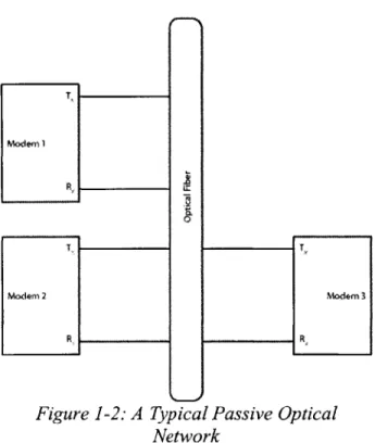
The primary difference between a classical optical network and a PON is that a PON is an
are many transmitters and receivers, as is shown in Figure 1-2. Modem 1 Modem 2 R 0 Modem 3 R
Figure 1-2: A Typical Passive Optical Network
In this network, there are 3 optical modems with full transmit and receive capability attached to
one optical fiber. This new configuration presents new challenges to the limit amplifier, and
addressing these new challenges will be the subject of this thesis.
1.2 Limit Amplifier Design Considerations
The major issue the limit amplifier must address is the varying input amplitudes and
offsets it must be able to accept while still performing correctly. These differing amplitudes and
-offsets arise from the varying power levels of received optical signals. If no photons are being
received by the photodiode in Figure 1-1, no current flows through it, and the transimpedance
amplifier outputs a baseline "dark level." If photons are being received, current flows through
the photodiode, and the transimpedance amplifier outputs a voltage that diverges, in one
direction or the other, from the dark level. How far the output diverges depends on the number
of photons received, and this in turn depends on the power of the transmitting light emitting
diode, the distance the photons have traveled, and impurities in the optical fiber. This leads to a
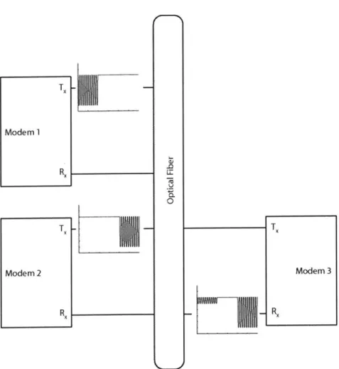
situation like that in Figure 1-3.
Modem 1 Modem 2 RX U. 0 Modem 3
Figure 1-3: Typical PON Functionality
In this case, modem 2 and 3 are close together, and modem I is far away. The power of
the signal sent from modem 1 is attenuated as it travels down the fiber, arriving at modem 3 with
much less power than the signal sent from modem 2. The resulting waveform is reproduced in
Figure 1-4.
d
t
F
w
Figure 1-4: Received Power Levels
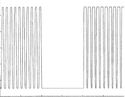
The question then becomes around which point to amplify the signal. If the signal is amplified
about the finely dashed line, in order to correctly amplify the low power signal, the resulting
waveform is shown in Figure 1-5.
-Figure 1-5: Correct Amplification for Low Power Signal
As can be seen here, the low power signal is correctly amplified. The high power signal, however, is distorted and more sensitive to noise. This will lead to significant jitter issues, which
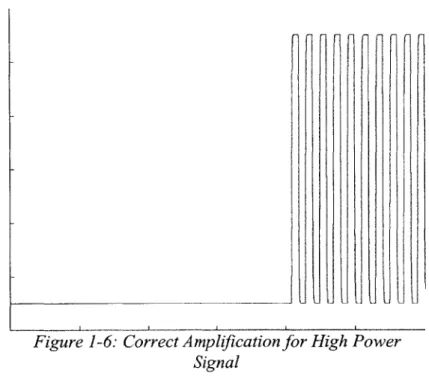
will cause the overall system to fail. The other option is to amplify the signal about the coarsely
Figure 1-6: Correct Amplification for High Power Signal
In this case, the high power signal is not distorted. The low power signal, however, is
completely annihilated, which is not acceptable either.
Given this, a good limit amplifier must be able to correctly determine about which level
to amplify the signal. It must perform this accurately, otherwise the signal will become distorted
and the jitter of the system will be too high. It must also perform this quickly, as in an Ethernet
the speed at which the system can switch between receivers is limited by the time it takes for the
receiver to adjust to a difference in offset level. Chapter 2 looks into previous approaches to
solving this problem.
-19-Chapter 2: Previous Work
As was discussed in the previous chapter, a limit amplifier in a passive optical network
must quickly adjust to changes in offset voltage. As classical optical systems have been
deployed for over a decade, limit amplifiers with automatic offset correction are not new. The
difficulty in going from a classical optical network to a more advanced passive optical network is
that, in a PON, the receiver must switch between many different sources. Classical systems
require as much as 1ms [2] of offset correction time, which is acceptable if the offset correction
is only run once at startup. If, however, the offset correction must be run every time another
modem wishes to transmit, this could lead to unacceptable latencies in the network. Of course, accuracy is also required, as the jitter requirements on many of these systems are stringent. In
this chapter, three previously employed topologies are considered, all of which will point the
way to a much faster system.
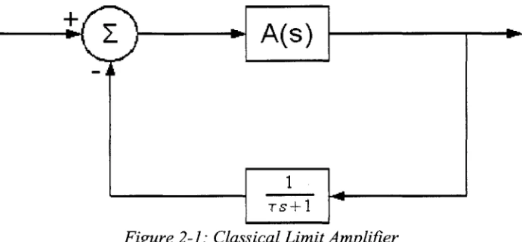
2.1 Classical Offset Correction
The most basic of offset correction techniques, and one that is employed frequently in
backbone one to one optical links, is to drive the mean of a signal to zero. This is accomplished
A(s)
TS+1
Figure 2-1: Classical Limit Amplifier
In this configuration, rather than choosing an appropriate level, a moving average is subtracted
from the input, and the result is then amplified about zero. This will guarantee that for any input
voltage amplitude and offset, the output is correct.
The main disadvantage with this scheme is that there is an inherent trade off between
jitter and offset correction time. For example, if a process were attempting to find the average of
a sequence of numbers that could either be a one or a zero, and averaging was done over the past
100 numbers, each successive bit received could only change the output by a maximum of 1%.
However, the system would have to wait for the first 100 numbers to come in to form a correct
average. To reduce the time required, the system could do an average on only 4 numbers;
however, this would mean each successive bit could change the output by up to 25%.
This phenomenon can also be seen in Figures 2-2 and 2-3.
-0 0.2 014 0.6 0.8 1 1.2 1.4 1.6 1.8 2
Time (s) X 10-8
Figure 2-2: Slow Moving Average
2 -16 1.4 1.2 0.8 0.6 0,4 0.2 0 0.2 0.4 0.6 0.8 1 1.2 1.4 1.6 1.8 2 Time (s) X 10
Figure 2-3: Fast Moving Average
In these figures, the trade off between average accuracy and average speed becomes clear. In
Figure 2-2, the average attains its final value more slowly but does not waver as much as the
average in Figure 2-3. Because this average will directly affect jitter, as is explained in [3], aggressive jitter requirements dictate a very slow average, making offset correction, or
compensation, times up to ims [2]. Another means of correcting for offset is therefore required.
2.2 Peak Detector Offset Correction
If, as is the case with many transimpedance amplifiers, fully differential signals are
available, a new method of detecting and correcting for offset becomes available. In this case, the maximum value the non-inverting output attains is
v in.mx = + vanp (2.1),
where v., is the offset voltage and vampi is the amplitude of the waveform. The maximum value
2 1.8 1.6 1.4 1.2 > 0.8 0.6 0.4 0.2 0
the inverting input attains is then
vin =-v +vampI (2.2),
implying that their difference is
V -V 2vos (2.3).
This is represented in Figure 2-4.
LJ J L. Ui
6 1 10
Time f a Bsx ltio > 10i0 Calculation Based on Peak Detection
Much of the jitter in the system from section 2.1 was caused by inter-symbol-interference
(ISI), in which the value of the output during one symbol period is directly affected by the
symbols the preceded it. Peak detection avoids this issue, as the speed at which the peak detector
acquires the maximum of the signal is largely decoupled with how much a non-peak value
affects the output. This is demonstrated in Figure 2-5.
-23 -06 (14 0 0 0,6 T
~1
I
L'
UI U 4 5 Figure 2-4: Offset2 - - - - - -- - -- -- ------ --- --- --- ---- -- - -1.8 - -1.6 -1.4 -1.2 -;M 1 > 0.8 0.6 -0.4 -0.2 -0 - - -- - - - - -0 0.2 0.4 0.6 0.8 1 1.2 1.4 1.6 1.8 2 Time (s) x 108
Figure 2-5: Input / Output Relationship of a Peak Detector
With this, the offset can be quickly corrected with a system, such as that from [4]. A
representation of such a system is shown in Figure 2-6.
V in+Pea k
Vs.l+ Detector
Peak Detector
Figure 2-6: Peak Detection Based Offset Correction
Figure 2-7.
Figure 2-7: A Bipolar Peak Detector
Because bipolar processes are considerably expensive, the question then becomes whether a
similar concept can be used in pure CMOS technology.
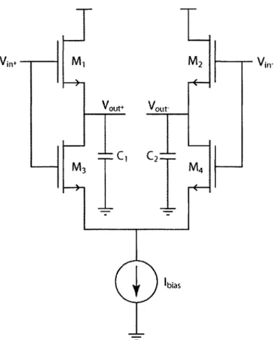
2.3 CMOS Peak Detector Offset Correction
As presented in [5], it is possible to use peak detector offset correction in a pure CMOS
process. This is primarily due to an improved CMOS peak detector topology developed in that
work, which is reproduced in Figure 2-8.
-Vin+ M, M2
Vin-vout+ vout.
C1 C2
M3 M4
I bias
Figure 2-8: An Improved CMOS Peak Detector
The exact functionality of this circuit becomes a major focus of this thesis, and is discussed in
section 3.2.3. The basic principle is that the circuit contains two source followers formed by M,
C1 and M2 C2. These source followers can be switched on and off depending on whether M3 or
M4 is carrying Ibias. For example, if vi,+ is greater than vin-, then vin+ is at its peak and therefore
should be sampled onto C1. Therefore, M3 will steal all of Ibias, causing M4 to switch off and C2
to hold its value. If vin- is greater than vin+, the situation is reversed.
In order to ensure that this happens, there must be a significant difference in voltage
topology, such as the one in Figure 2-9, is required.
Integrator Analog Mux
select & Vpeak+
Select
Logic 4 Vpa
Integrator Analog Mux 4k
Vpeak 1+ Vpeak2+ Vek3+
Peak I- Peak Peak
Detector Vpeaki Detector Vpeai2 Detector Vpeak3
In
Av
A
A
Out
Vos
Figure 2-9: System from [5] (Figure from [5])
In this case, a multistage amplifier with multiple peak detectors is employed. A large enough voltage differential is required in order to make the circuit from Figure 2-8 function. If, however, the output voltage from the amplifier saturates, this will introduce nonlinear dynamics into the loop. Therefore, the largest non-saturated pair of outputs must be selected by the analog multiplexer (mux). Because the peak detector dynamics are nonlinear, a loop compensator must be employed, which in the case of this system is an integrator. However, if a constant gain integrator were used, the loop gain could depend on which peak detector was selected.
-27-Therefore, the integrator is a variable gain integrator, with its gain being set by the number of
amplifier stages in the loop.
This compensation scheme has been successful in reducing offset compensation times to
less than 1 [ts, while still retaining good jitter performance in CMOS. While this is a three orders
of magnitude improvement over the system in 2.1, it is still not enough. Many PONs call for the
ability to connect up to 256 optical modems to one optical fiber. If each transmission takes 1 ps
for offset correction, and latency is to be kept under lms, this means that 25% of the available
time for data transmission is taken up by offset correction times. A new goal of 20ns has
therefore been set by the industry. Of course, the limit amplifier is not the only element in the
receiver from section 1.1, and therefore cannot consume the entirety of this budget. The goal of
this thesis will thus be to reduce the compensation time to less than 20ns.
The question that comes to mind is whether any of the previously presented systems can
be modified to meet this goal. The system from section 2.1 clearly cannot, as the trade off
between jitter and speed is a mathematical certainty. The system from section 2.2 could, but
implementations would rely on expensive BiCMOS processes. To understand whether the
system from section 2.3 could be modified to meet this goal requires a greater understanding of
the circuits it employs. Therefore, the next chapter will develop accurate models of those
circuits, with the aim of redesigning the system to meet the more aggressive goal for offset
Chapter 3: Analog System Modeling
While the system described in section 2.3 was a vast improvement over previous efforts, newer PONs require offset correction times of less than 20ns to achieve acceptable latencies in
the overall network. Given the cost of fabricating test systems, accurate models are required to
aid in the design of aggressive analog systems. Component-level simulators, while accurate, require immense numbers of computations, and therefore behavioral-level simulation is required.
In this chapter, highly accurate behavioral-level models are developed for complex
analog systems and compared to component-level simulations to test their validity. These
models will then be used in chapter 4 to develop a system meeting the desired 20ns settling time.
3.1 Motivation for CPPSIM
While component-level simulators such as SPICE and SPECTRE have become
exceptionally accurate, they have done this by increasing the complexity of the algorithms they
use, causing them to be relatively time consuming. Due to the high level of complexity of the
system in question, transistor-level simulations of the entire circuit could take hours or even days
to complete. This, along with the fact that many of the transistors are coupled together into
highly-linear blocks, points towards a higher level of simulation being required.
Behavioral-level simulators, such as CPPSIM, fulfill that role. Simple blocks, such as the
integrator, can be modeled by a single multiply-accumulate function. More complex blocks, such as the saturating amplifiers and peak detectors, may require more complex computations.
-If, however, they can be accurately modeled by even one hundred intelligent computations, there
will be a significant improvement in simulation speed. The process then becomes to partition the
overall system into subsystems, develop a computational model for them, and check that the
response of the computational model is very close to the response of the transistor-level model
for relevant inputs.
These models can then be altered to observe the effects of changing system-level
parameters without having to redesign low-level components. For example, in a transistor-level
model, placing arbitrary poles and zeros in the loop compensator would require an altered
op-amp for each configuration desired. However, in a behavioral-level simulator it would only
require adding a "pole" or "zero" block to the overall loop. CPPSIM was chosen as the
behavioral-level simulator due to its large preexisting library, the ease of designing
computational models in C++, and the fact that the previous system from section 2.3 was
modeled using the same software. For more information see
http://www-mtl.mit.edu/researchgroups/perrottgroup/tools.html.
3.2 System Block Modeling
As was discussed in section 3.1, accurate computational models of the subsystems are
required to form an accurate behavioral-level model. In this section, accurate behavioral-level
models are developed for the major components of the system in 2.3: the amplifier, the loop
compensator, and the peak detector. While the models developed in [5] are accurate for the
simple low frequency pole. Special attention to the large signal and small signal performance
points towards a more complex and accurate model.
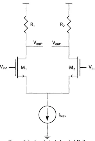
3.2.1 Amplifier Modeling
Much of the amplifier design for this work is borrowed from [5] and is detailed in section
4 of that work. At the core of the amplifier is the structure shown in Figure 3-1.
R, R
2
Vout. Vout
Vin+ - M M2
Vin-Ibias
Figure 3-1: A resistively Loaded Fully Differential Amplifier
-This is a standard resistively loaded fully differential amplifier, having a dominant pole at
1 1
and a high frequency zero at R An important feature of the limit amplifier is
RCL RCgs
that at least the final amplifier must saturate, and therefore the model must include some way of
representing this. Due to how the loop functions, however, this modeling does not need to be
exceptionally accurate. As is described in sections 2.3 and 3.2.2, the loop rejects any saturated
signals, and therefore accurate modeling would be wasted computation, as the results would not
be used. Of course, the noise produced by the transistors and resistors cannot be neglected.
Rather than insert noise into each stage of the amplifier, the total noise is input referred. This
allows one to quickly see the overall effect of improving the noise performance of individual
components. The final model is included in the tutorial available online at
http://www-mtl.mit.edu/researchgroups/perrottgroup/tools.html.
3.2.2 Loop Compensator Modeling
The loop compensation in this system is highly complex and nonlinear; however, its
function can be easily described by a behavioral-level model. The system as a whole is shown in
Integrator Analog Mux
slect & Vek
Select
Logic
Vpeak--- Integratr J4-- Analog Mux
Vpeak1+ Vpeak2+ Vpeak3+
Peak Peak Peak
Detector Vpeak1- Detector Vpeak2 Detector
Ypeak3-In
A
A
Av
Out
Vos
Figure 3-2: System from Section 2.3 (Figure from [5])
To review from section 2.3, the output of each peak detector is fed into an analog multiplexer.
The signal that is output from that multiplexer is the largest pair of input signals for which
neither one is saturated. The resulting differential signal is then fed into a number of integrators, the number of which is determined by which peak detector output was selected, and then it is
added to the input signal to cancel the offset. The purpose of using multiple integrators is to
maintain constant loop gain, regardless of which peak detector is selected.
Realizing this, instead of modeling every component of this highly complicated loop
filter individually, the same results can be achieved by breaking the filter down into three less
complicated blocks. Of course this is not how the final solution would be implemented, but
-rather a model that simplifies simulating and modifying the design. The first block that must be
implemented is the selector, a module already available in CPPSIM. The selected output, rather
than being fed into a variable gain integrator, forms the input to a variable gain block with no
dynamics. The resulting signal is then fed into a constant gain loop compensator, as is shown in
Figure 3-3. Vpeak1+ Vpeak1~ V V,,i++qk2 peak2 V + VpeaI(7
Figure 3-3: Simplified Model of System from Section 2.3
With this modification, the designer can arbitrarily choose the linear compensator from any of
the already available modules in CPPSIM or create his own with relative ease, without changing
the accuracy of the simulation. Select
3.2.3 Peak Detector Modeling
While [5] contained accurate models for the amplifier and loop compensator, it used a
low frequency pole to model the action of the peak detector. This section details the complexity
of its operation, and develops an accurate behavioral-level model based on the intuitive
functioning of the circuit.
At the core of the design is the improved CMOS peak detector, shown in Figure 3-4.
Vout+ Vor
C1 C2
M3 M4
--Fbias
Figure 3-4: Improved CMOS Peak Detector
-This peak detector functions by sampling whichever input, vin+ or Vin-, is higher and holding the
other at its previous value. For example, if vin+ is higher than Vin-, then M3 will steal all of lbias,
and M, and C1 will form a source follower. At the same time, M4 will be cut off, and therefore
C2 will hold its voltage. The situation becomes reversed when vin- is higher than Vin+ In this
case, M2 and C2 form a source follower, while, Ci holds its previously stored value.
The dynamics of the system are slightly more complicated. The source follower has
dynamics governed by the small signal model shown in Figure 3-5.
Vin
Vgs Cgs 9mVgs
C,
Figure 3-5: Small Signal Model
gmn The speed at which the source follower achieves its final value is governed by the C ratio
of the transistor and load capacitor. Due to the high data rate, this time constant can be smaller
than a symbol period and can therefore significantly affect the performance of the system.
Furthermore, the switching of sampling and holding is not instantaneous. For example, there will be a period of time when vi,+ is still higher than vi,- but is lower than its peak value.
During this period, the source follower will still try to track the input signal, and will (if the
transition is reasonably sharp) slew. This is demonstrated in Figure 3-6.
01 008 0.0B 004 0.02 0 -002 -0.04 -0.06 -0.08 ( (1 II 0.8 1.2 1m4 Time (s) 16 1,8
.10-Figure 3-6: Peak Detector Response
This implies two things. First, an accurate model must take into account the transition period,
and second, the jitter of the peak detector still depends on the 'bias ratio. The effects of
C
this will be discussed in further detail in section 4.1.
The final model for the peak detector is available in the tutorial online at
http://www-mtl.mit.edu/researchgroups/perrottgroup/tools.html, and is included as pseudo code
below:
-37
if(vin+ > vin-) {
vout+ = source follower(vin+);
vout- = capacitive coupling(vin-);
if(vin- > vin+) {
vout+ = capacitive coupling(vin+);
vout- = source follower(vin-);
In this case, the source follower model must account for finite slew rate and gain, as well
as the direct capacitive coupling provided by Cgs and C1. While this does not model the system
completely, simulations show that it provides a nearly perfect representation of the peak
detector's response, as is detailed in section 3.3.
Furthermore, many of the errors this simplification introduces cancel each other out. For
example, while M3 and M4 do not completely switch when vin+ is equal to Vin-, the amount by
which M3 should be "less on" during a transition from vin+ being high to both signals being equal
is about the same amount by which M3 should be "more on" while vi,- goes from being equal to
vi,+ to being high, as is shown in Figure 3-7.
Approximation
Actual
Figure 3-7: Straight Line Approximation
In this figure, the hatched areas above and below the straight line approximation have equal
areas, indicating that the integral of the error introduced by the straight line approximation is
zero. Because these transitions are so fast, the non-integral error is out of band and therefore
does not affect the overall functioning of the circuit.
Thus a highly accurate model for the improved CMOS peak detector has been developed.
A wide variety of component nonidealities, such as capacitive coupling and finite gain, have
been taken into account. While this is not an exact model, the next section will show that it is
acceptably accurate over the range of inputs it will experience while employed in the overall
system.
3.3 Device-Level Modeling
Accuracy of these models was confirmed via testing in SPECTRE, using design
parameters provided for IBM's 0.13pm process. Given the accuracy with which the limit
amplifier and loop compensator were modeled in [5], verification of these components was not
necessary. Given identical inputs, simulations in SPECTRE and CPPSIM show similar outputs, which can be made nearly identical by tweaking modeling parameters in CPPSIM.
Shown in Figure 3-8 is a comparison between the responses of the device-level model
and the behavioral model when given a 1.25GHz input square wave.
-0.09 0.0-0.07 0.06 0.9 095 1 1.05 1.1 Time (s) 10,
Figure 3-8: Response of Both Simulators to a 1.25GHz Square Wave
This figure shows similar behavior in both models given an input wave that changes as quickly
as a 2.5Gbps input signal could possibly change. Figure 3-9 shows the response of both models
to a slow input waveform, which gives a much clearer representation of exactly what happens
0.1 I I I I 0.08$-0.04 -002 - 0--002 --0.04 -0.06 -0.08 --0. 8 1.2 1.4 Time (s) 1.6 1.8
Figure 3-9: Response of Both Simulators to a 25MHz Square Wave
To achieve such close results, the slew rate and the location of the dominant pole were
extracted from the component-level simulation and used in the behavioral-level simulation.
Thankfully, the slew rate is exceptionally close to CL , and the location of the dominant pole
to . This allows designs to be easily modified without having to check the exact slew
nkTCL
rate or dominant pole location after each minute change in parameters.
-41-0.1
1
In this chapter, accurate models for the primary system components from section 2.3 have
been developed. A complete overhaul of the peak detector model has led to near perfect
agreement between device and behavioral-level simulations. While these models are
significantly more complex than the simple linear models proposed by [5], the improved
accuracy will allow for more aggressive systems to be designed, while the nature of behavioral
Chapter 4: Analog System Design
In this chapter, a design capable of 20ns offset correction time, with only 2.30ps RMS
jitter in response to a 1OmV input, will be presented. This will be accomplished by modifying
the system from [5] to use a more aggressive compensation scheme as well as a more highly
tuned peak detector. Linear models will be developed for the system to aid in design, while
behavioral models will be employed to simulate the system more accurately.
4.1 Peak Detector Design
The performance of the peak detector directly affects the performance of the system as a
whole, and therefore careful attention must be paid to its design. If the peak detector is too
slow, compensating the system for 20ns offset correction time will be impossible. However, if
the peak detector is too fast, the system may produce unreasonably high jitter. This section
focuses on attaining an acceptable balance.
As was discussed in section 3.2.3, the peak detector (shown in Figure 4-1) has highly
complex dynamics.
-4u 4u ViM1120n 120n M2 V1 n-vout+ vout C1 C2 -M3 400fF 400fF M4 2Lj 2 u 120n 120n S bias SpA
Figure 4-1: Improved CMOS Peak Detector
Because M3 and M4 do not switch instantaneously, and because the input signals do not transition
between their high and low voltages in a step-like fashion, output of the peak detector will slew
bias
downward with a slope of
C
during the transition. It might seem from this that theimproved CMOS peak detector struggles from the same problem faced by the CMOS source
follower, in that there is a trade off between fast performance and low droop. This trade off is
improved, however, in that the new design only droops at that high rate during transitions, whereas the traditional design droops throughout the entire period in which the input signal is
'M bias
This, however, does mean that we want to have the largest C to
C
ratiopossible, meaning that M, and M2 should be in weak inversion. Unless some slew rate limiter is
introduced, the best ratio that can be achieved is
1
gm2 -r C -rr I - gM m ~ I qq (4.1).
Ibias 2 Tr Ibias 2r nkT C
Measured results indicate this number is close to 5.5 in 0.13pm CMOS; however, it is a fixed
number regardless of changes to Ibia, or C. Because this number directly influences the
fundamental figure of merit of the limit amplifier, if it were improved, a better limit amplifier
could be designed. However, most slew rate limiters rely on components that are not available in
a CMOS process. Furthermore, the performance of the system was not limited by the peak
detector. For these reasons, the peak detector topology was left as-is.
What this trade off does mean is that the pole introduced by the peak detector should not
be used as the dominant pole, as then the jitter associated with slewing would be in-band. This
has two implications: first, a linear model of the peak detector must be ascertained, and second, the peak detector should be as fast as possible, such that it does not negatively affect the
performance of the loop. As the linear model will only be used as a rough basis for a design, it
does not need to be as accurate as the behavioral model.
Because the dominant pole of the peak detector will always be much slower than the data
rate, one could use a single pole to model the system. However, the incoming data will consist
of zeros and ones according to a random pattern, and the peak detector / sample hold will not
-45-always be in its sample phase. If the peak detector receives an average of half ones and half
zeros, the source follower will be in the signal path about half the time, which is analogous to a
sample and hold that is half as fast being in the signal path the whole time.
This, however, has some other issues. Over small periods of time, on the order of a few
tens of time constants, the peak detector could receive significantly more ones or significantly
more zeros, as there will only be 2.5 symbols per nanosecond at a data rate of 2.5Gbps. This
could mean one peak detector would be on for more or less than exactly half the time, leading to
a different average pole location. Therefore, the model must take into account the possibility of
a data-dependent moving pole. This is represented in Figure 4-2, in which possible pole
locations are traced out.
Bode Diagram
2C2
S40
10 0 10
10-Frequency (rad/sec)
Of course, the representation above is not entirely accurate. An important aspect of the
peak detector is that there are two signal paths, one of which samples while the other holds its
previous value. If one path is sampling less than expected, it will adjust to offset slower than
expected, bringing its pole in closer to the
j-o
axis. The other path, however, will be samplingmore than expected and thus pushing its pole away from the
j-o
axis. Therefore, the modelshown in Figure 4-3 is more accurate.
1
T., s+
Figure 4-3: More Accurate Linear Model
In this model, the "fast" path (the one containing rf) acts to correct the "slow" path. Therefore, the bode plots more closely resemble those in Figure 4-4.
-Bode Diagram 10 0 -10 -S-20 -30 0 --90 H 10 10 10 10 10 10 Frequency (radfsec)
Figure 4-4: Bode Plot of Improved Linear Model
As this implies, the more one path is favored over another, the stronger a doublet will exist in the
transfer function. This is to be expected, since if one path of the peak detector were holding, the
loop would be able to "mostly" settle. However, the loop would need to wait for the slow path to
reach its final value before it could completely eliminate any offset.
Thankfully, complete settling may not be required. Because the limit amplifier will
saturate, correcting the offset exactly is not necessary. Furthermore, as more symbols are
received, the probability of receiving many more ones than zeros becomes vanishingly small.
issues moot. Therefore, loop designs must only reflect the case in which rf and T, are equal, as other loops will remain stable but have an unavoidable long tail settling produced by the very visible doublet in Figure 4-4.
Given these constraints, the peak detector pole should be placed at as low a frequency as
will be allowed by the overall loop compensation. It cannot, however, be the dominant
compensation in the system. This indicates an optimal speed - fast enough so as not to degrade
loop performance, but no faster. The pole introduced by the peak detector in this design is at 120MHz, which does not degrade jitter performance, but allows for 20ns settling times. As was discussed earlier, this indicates that loop compensation schemes must adjust for a dominant pole
location of 60MHz, and such compensation schemes will be discussed in the next section.
4.2 Loop Design
In this section, three linear compensation schemes are presented: the single pole
overdamped compensation scheme used in [5], a single pole aggressive configuration, and a
lag-lead advanced compensation scheme. The advantages of each configuration are discussed, with attention paid to the variability of pole and zero locations due to process variation. In all designs, a constant loop gain of 80dB with a non-dominant pole location of 60MHz is assumed. This results in an optimal configuration of a dominant pole at 4KHz, with a compensating zero at
50MHz.
-4.2.1 Overdamped Loop Compensation
A good starting point is the compensation scheme used in [5]. The loop compensation
used in this work is an integrator; however, as no physical component has infinite DC gain, a
more accurate model is a 1st order low-pass filter with high DC gain. The design uses a 40dB
amplifier with a pole at 100Hz, producing the bode and step responses shown in Figure 4-5.
Bode Noeru
--- - -- ..-- ..- ---. - ,
-I*5
.' 10' 130 ~ i i
Frequency (red/sec)
Figure 4-5: Bode and Step
Step Response
0O)-01 0.2 03 0.4 05 06 0.7 0 09
Time (sec)
Response of System from [5]
Because the compensation approach used here is highly conservative, the result is a very stable,
but very slow, step response. This is desirable if compensation time is not a primary concern, as
varying pole locations cannot drive the system into an unstable configuration. However, it
comes nowhere close to meeting the desired 20ns settling time, and therefore another
compensation scheme is required.
4.2.2 Aggressive Loop Compensation
The question is whether or not a less conservative compensation scheme can achieve
significantly faster responses, while still maintaining loop stability and low jitter. Linear control
theory states that to achieve the fastest possible step response, the loop should be critically
damped. Of course, a good design must be robust to process variation. While good layout
techniques can eliminate much of this variation, allowing for ±25% mobility in all pole and zero
locations is necessary to ensure the final product will function. Therefore, plots in this section
will reflect all possible process corners a design may encounter. Shown in Figure 4-6 are the
step responses of the aggressively compensated loop, in which a pole at 1KHz is used.
Step Response -- - -- - - // - --- /-- - - ---- 'UI S0A0 04
02-
l/
0 I I I I 0 0,5 1 1.5 2 2,5 3 3.5 4 4.5 5 Time (sec) x 10Figure 4-6: Step Response of the Aggressively Compensated Loop
-In this case, some of the possible pole locations lead to exceedingly fast offset correction;
however, others can take unacceptably long. This type of design could be useful if fabrication
processes become more controlled, or if post fabrication testing can eliminate those chips that are
unsuitable for 20ns offset correction times. To keep cost low in current processes, however, another method of loop compensation is required.
4.2.3 Advanced Loop Compensation
Advanced loop compensation in the form of lag-lead compensation produces the results
required. With a pole at 4KHz and a zero at 50MHz, step responses such as those in Figure 4-7
are produced. Step Response o A 0.2 0 0 5 1 1.5 2 2.5 3 35 4 4.5 Time (sec)
Figure 4-7: Lag-Lead Compensation Example
5
/ - -
While the doublet produced by these parameters is still highly visible, the overall settling
time achieved is much faster. Despite highly variable pole and zero locations, all process corners
settle to within 2% in 20ns. With this, a final design that can be verified in behavioral-level
simulations has been generated, and in the next section it will be verified that it produces the
desired results.
4.3 Behavioral-Level Modeling
In this section, the designs from section 4.2 will be tested using a behavioral-level
simulator. Given the peak detector's nonlinear nature, as was discussed in section 3.2.3, these
simulations are necessary to verify that the chosen compensation scheme will in fact work.
Results similar to those from section 4.2 are observed, verifying the use of linear models to
describe the system. These simulations indicate 20ns settling time is possible, with the dominant
source of jitter being the noise injected by the amplifier.
To fairly judge the performance of each topology, one must consider the jitter injected by
each component individually. Therefore, the results presented in this section reflect the
performance of a totally noiseless system, and therefore are not achievable results. The total
jitter in the final system will be discussed in section 4.4.
4.3.1 Overdamped Loop Compensation
In the overdamped case, the behavioral simulator produces results very similar to those of
-the linear model. This is to be expected, as in -the overdamped case -the non-dominant pole
barely asserts any influence on the overall transfer function. The results from the behavioral
simulator very closely resemble those from the system implemented in [5], which if nothing else, offers assurances that the model is functioning accurately. These results are represented in
Figure 4-8, which has 11 Ifs RMS jitter.
-o U) C-) a) U) Q U) a)) Ca 0 (C) 0 -1 -2 -3 -4 -5 -6 X 10'3 - -o
-K
-7 I I I I I I I I 0 0.1 0.2 0.3 0.4 0.5 0.6 0.7 0.8 0.9 1 Time (s) X 10-6Figure 4-8: Behavioral Response to Overdamped Loop
4.3.2 Aggressive Loop Compensation
In the aggressive case, the results from the behavioral simulator diverge slightly from the
weighing in more heavily on the loop dynamics. Shown in Figure 4-9 is the step response of the
behavioral model, which has 41 fs of RMS
jitter.
These simulations clearly show a simpledominant pole compensation technique is not sufficient for 20ns settling times.
a) 0 a) a) Q a) (1, 0 a) C,) 0 0 -1 -2 -3 -4 -5 -6 -7 0 0.1 0.2 0.3 0.4 0.5 0.6 0.7 0.8 0.9 1 Time (s) x 10 7
Figure 4-9: Behavioral Response to Aggressive Loop
4.3.3 Advanced Loop Compensation
The advanced loop compensation meets the desired settling time of 20ns. Typical
responses of process corners are shown in Figure 4-10, which have an average 626fs RMS jitter.
- 55 -X 103
x 0* 0 a)-3-a--3 0 -7 0 0.1 0.2 0.3 0.4 0.5 0.6 0.7 0.8 0.9 1 Time (s) x 107
Figure 4-10: Behavioral Response to Advanced Loop
While the response is certainly not linear, the loop does acquire the correct offset voltage within
the time allotted. There is considerable variability in the output voltage, which is due to the trade
off between peak detector speed and jitter discussed in section 4.1. Because the loop is so
aggressively compensated, the peak detector dynamics do affect the performance of the loop, and
the result is a varying output waveform. Thankfully these variations are small enough so as not
4.4 Results
Because jitter, like noise, can be modeled as a random white process, it adds as
jitter (total)
\I
jitter' +jitter'
(4.2).Therefore, the only efficient method to reduce jitter is to reduce the largest source, rather than
attempting to optimize every other element in the circuit. Despite being well-designed, the jitter
from the amplifier from [5] alone contributes 2.23ps of RMS jitter to the output, which accounts
for almost the entirety of jitter found in [6]. This implies that, despite the exceptionally
aggressive loop compensation employed in 4.3.3, the steady state performance of the limit
amplifier has not degraded appreciably. Running the behavioral simulation and including the
noise from the amplifier and peak detector, the RMS jitter only increases to 2.30ps, indicating
that equation (4.2) is indeed correct.
With this, a complete design for an analog system to correct offsets in less than 20ns has
been proposed and simulated. The accuracy of the simulations has been confirmed by
comparing results to those from component-level simulators, as well as from previous tests in
silicon. While not all component nonidealities have been included, care has been taken that
these do not affect the performance of the system in any significant way. Therefore, the system
described should function as planned when implemented.
-Chapter
5:
Digital System Overview
While the previous two chapters developed an analog system capable of 20ns
offset cancellation, the resulting system was heavily dependent on sensitive analog circuitry.
This can be seen in the varying step responses of the system based on 25% variation in pole and
zero location. Therefore, this chapter develops a digital system capable of instantaneous offset
correction, with the downside of degrading the functionality of the clock and data recovery unit.
Several possible topologies are discussed, and a more detailed design of one of these is presented
in chapter 6.
5.1 Basic CDR Structure
To understand how a discrete time digital limit amplifier can replace a continuous time
analog limit amplifier, a good understanding of the clock and data recovery (CDR) unit is
required. This is due to the fact that, in an optical receiver, the CDR is the only system block
that uses the output of the limit amplifier, and therefore it dictates the requirements placed on the
limit amplifier.
At the core of every CDR is a phase-locked loop (PLL), which has the basic structure
Phase
Detector
Oscillator
H
Figure 5-1: Basic Phase-Locked Loop Structure
The phase detector does as its name implies - detects the difference in phase between the input
and output waveform of the PLL. This difference is fed through some (possibly nonlinear) loop
compensator, which in turn controls the frequency of the output oscillator. If designed correctly, the loop will drive the difference in phase between the two waveforms towards zero, thus
"locking" the two waveforms to have identical frequency and phase. With this, the CDR can
recover the original clock and data, as is shown in figure 5-2.
- 59
-Loop
Sample on Falling Edge
Data
Recovered
Clock
Synchronize Rising Edge
Figure 5-2: Recovering Data
from
a Bit StreamDesigning loops to quickly acquire and accurately hold onto the clock frequency and
phase used to encode the data stream is an active area of research. Therefore, a limit amplifier
designed in a vacuum must accurately amplify the entire input waveform, as the exact nature of
what the CDR requires may vary from design to design. It may be of use, however, to
understand some of the more commonly used phase detectors, as that is the part of the CDR
which must interact with the limit amplifier.
5.2 Common Phase Detectors
When choosing an appropriate phase detector for such a system, there are several
computations should be avoided. Second, during any clock cycle a transition may or may not
occur, and that transition may be rising or falling, as is shown in Figure 5-3.
Rising Edge
No Edge
Falling Edge
Data
Recovered
Figure 5-3: Issues Faced by the PLL
These requirements are satisfied by two of the most commonly used phase detectors in
communication systems: the Hogge detector and the Alexander (bang-bang) detector. These
phase detectors are shown in Figure 5-4.
-61-Hogge Detector (Linear) Bang-Bang Detector (Nonlinear)
...e(t) Reg Reg retimed
-data(t)dtat
D Q D Q
clk(t) e(t)
Reg Latch retimed Reg Latch
data(t.) data(t)
DQ D Q D Q D Q
clk(t) clk(t)
Figure 5-4: Two Commonly Used Phase Detectors (Figure from [7])
Each phase detector has its own advantages, and a good limit amplifier should be able to support
either of them, or even another topology, if need be. Both designs do, however, share a common
trait: they both latch the input signal based on the recovered clock. Because of this, the value
output by the limit amplifier is only relevant at twice the clock frequency. Furthermore, the
exact value is not relevant, only whether value transmitted was "high" or "low." Both of these
facts point towards a discrete-time digital implementation of the limit amplifier.
5.3 Digital Limit Amplifier Topologies
Given the new constraints on the limit amplifier - a small input signal, a digital output
signal, and a clock indicating when the output must be computed - it becomes clear that a good
![Figure 2-9: System from [5] (Figure from [5])](https://thumb-eu.123doks.com/thumbv2/123doknet/13882877.446900/27.918.99.789.220.613/figure-system-from-figure-from.webp)
![Figure 3-2: System from Section 2.3 (Figure from [5])](https://thumb-eu.123doks.com/thumbv2/123doknet/13882877.446900/33.918.101.787.136.523/figure-section-figure.webp)
