HAL Id: hal-03067854
https://hal.archives-ouvertes.fr/hal-03067854
Submitted on 30 Dec 2020
HAL is a multi-disciplinary open access
archive for the deposit and dissemination of
sci-entific research documents, whether they are
pub-lished or not. The documents may come from
teaching and research institutions in France or
abroad, or from public or private research centers.
L’archive ouverte pluridisciplinaire HAL, est
destinée au dépôt et à la diffusion de documents
scientifiques de niveau recherche, publiés ou non,
émanant des établissements d’enseignement et de
recherche français ou étrangers, des laboratoires
publics ou privés.
Surface-Electrode Ion Trap With Ground Structures for
Minimizing the Dielectric Loss in the Si Substrate
Jing Tao, Hong Yu Li, Yu Dian Lim, Peng Zhao, Anak Agung Alit Apriyana,
Luca Guidoni, Chuan Seng Tan
To cite this version:
Jing Tao, Hong Yu Li, Yu Dian Lim, Peng Zhao, Anak Agung Alit Apriyana, et al.. Surface-Electrode
Ion Trap With Ground Structures for Minimizing the Dielectric Loss in the Si Substrate. IEEE
Transactions on Components, Packaging and Manufacturing Technology, Institute of Electrical and
Electronics Engineers, 2020, 10 (4), pp.679-685. �10.1109/TCPMT.2019.2958661�. �hal-03067854�
Surface Electrode Ion-Trap with Ground Structures for
Minimizing the Dielectric Loss in the Si Substrate
Jing Tao, Hong Yu Li, Yu Dian Lim, Peng Zhao, Anak Agung Alit Apriyana, Luca Guidoni and
Chuan Seng Tan, Senior Member, IEEE.
Abstract—Surface electrode ion trap is one of the key devices in modern ion trapping apparatus to host the ion qubits
to perform quantum computation. Surface traps fabricated on silicon substrate have the versatility for complex electrode fabrication with 3D integration capability. However, Si induced dielectric loss needs to considered for trap design and the additional ground structure is necessarily incorporated into the surface electrodes fabrication. In this work, surface electrode ion trap is fabricated using standard Cu back end process on a 300-mm Si wafer platform. Several process novelties are demonstrated: (1) the use of electroplated Cu/Au layers using microfabrication techniques to form the surface electrodes, (2) the use of dry etching to form the fine gap oxide trench between the electrodes for reducing the charge induced stray electric field, (3) the use of Cu mesh ground structure to enhance the resonance performance of the trap, and (4) process optimization to minimize the undercut in Cu/Au electrodes. Promising electrical properties is obtained from the fabricated ion trap, with leakage current failure rate of < 10% on a 300-mm wafer. Two trap types designed with RF line widths of 80 and 40 μm are evaluated for their resonance performances without and with ground plane. By incorporating ground plane into the ion trap, the resonance performances are significantly improved with output power increment of 11 and 13 dBm and Q factor increment of 2 and 6, for the corresponding trap types.
I. INTRODUCTION
Ion trapping device [1]–[4] has been extensively reported to possess promising features in
realizing scalable quantum computers. By utilizing combinations of static (DC) and radio-
frequency (RF) fields, ion qubits can be physically confined in vacuum space and quantum
computing operations can be performed by transiting the internal atomic energy levels of the
qubits using lasers with some specific wavelengths. Due to its capability in precise
manipulation of multiple ion qubits with high fidelity and long coherent time, ion trap devices
have drawn many attentions among the quantum computing and engineering communities.
In a typical ion trap quantum computing device, the ion qubits are physically trapped by a set
of DC and RF electrodes, which generate a trapping electric fields to confine the ion in X, Y,
and Z directions. The ion qubit will be trapped at a position at the minimal pseudopotential,
as visualized in Fig. 1. The trapping ion position is mainly determined by surface electrode
geometry, where ion height depends mainly on RF line width and the space between the two
RF lines.
One of the pioneering ion traps is linear Paul trap [5], which is composed of a set of
macroscopic electrode rods in a linear quadrupole arrangement for the exertion of confining
electric fields. However, the bulkiness of conventional Paul trap limits its flexibility in building
complex, highly integrated quantum computing systems. As the advancement to traditional
Paul trap, surface electrode ion traps with arbitrary electrode configurations in the same plane
of substrate surface with single or multi-zone ion traps have been introduced. Surface
electrode ion trap fabricated on an insulator substrate was first proposed and demonstrated
by the NIST group in 2005 [6]. The advantage of such chip trap over the traditional linear Paul
trap is the use of microfabrication capability to enable complex trap design with multiples
electrodes. However, the fabrication of such chip trap involves heavy substrate etching
processes and MEMS fabrication techniques which may not be viable for seamless electronics
and photonics integration on the same chip. Surface electrode ion traps fabricated on silicon
substrate with dedicated electrode configurations have later been demonstrated by Sandia
high-optical access (HOA) and Y- junction traps [7], [8] and Georgia Tech/Honeywell ball-grid
array (BGA) trap [9]. These traps are designed with multiple and irregular DC electrodes and
fabricated with multilayer metal structures to facilitate precise ion control and shuttling with
enhanced trapping performance. Apart from these, new types of ion traps such as
microwave-controlled electrode trap [10] and surface trap with tunable ion distance [11] have been
demonstrated by other research groups. Due to the increasing complexity and diversity
requirement imposed on the surface trap design, the consideration to incorporate the trap
fabrication into a more foundry compatible, large-volume and fast turn- over time production
to prove the design concept becomes imperative.
In this work, we fabricate the surface trap using a main- stream 300-mm Si wafer in standard
foundry conditions. The Cu backend process is employed to fabricate a thick and flat trap
electrodes. The SiO2 insulation layer between the electrodes is dry etched to reduce the
electrostatic charges induced stray fields. To address the parasitic coupling induced by Si
substrate, a ground plane is designed and fabricated in the ion trap. The fabricated traps are
then tested to examine their compliance with the required resonance performance for proper
operation of the ion-trap.
II. SURFACE ELECTRODE FABRICATION
Surface electrode ion trap fabrication is accomplished on standard 300-mm Si wafer platform.
Four trap types are included in one layout design. The traps are designed with similar
geometries but different RF line widths and spaces, which result in different trapping ion
heights. Table 1 lists the trap geometrical specifications with simulated ion heights for each
trap types. For trap fabrication, two important process steps are: (1) SiO2 insulation layer
patterning and dry etch, and (2) Cu/Au metal layer patterning and electroplating. Fig. 2 (a)
shows the Scanning Electron Microscopy (SEM) images of the patterned SiO2 pads with
overall, magnified and titled view. The insulation layer is formed by 3 μm thick low-stress
Plasma- enhanced chemical vapor deposition (PECVD)-deposited SiO2. SiO2 in the electrode
gap area is patterned and dry-etched to reduce the effective exposed dielectric surface to the
ion and the stray electric field around ion-trapping region [12]. Cu/Au electrode is
subsequently aligned, patterned and electroplated on top of SiO2 pad. Fig. 2 (b) shows the
microscopic top overview, SEM top magnified and titled images after the Cu/Au electrodes
fabrication. The metal electrodes are recessed by 1 μm to the SiO2 pads. Au is directly
deposited on Cu layer as surface passivation layer to control the amount of Cu oxidation. The
inter-diffusion of Au and Cu is studied by X-ray photoelectron spectroscopy (XPS) analysis
which will be discussed in section B.
A. Cross-sectional Analysis
The cross-sectional SEM views of ion trap electrodes with four layers and the inter-electrode
gap area are shown in Fig. 3 (a) and (b), respectively. The designed and measured dimensions
of the electrode layer and gap are summarized in Table II. The SiO2 layer thickness is optimized
to be ~3 μm, juggling between acceptable stress-level for full-wafer fabrication, and sufficient
thickness to address the parasitic capacitance issue in Si substrate. Ti/Cu is deposited as the
barrier layer and seed layer for Cu electroplating. A thick Cu layer of > 3 μm is electroplated
to further hinder the ion sight to the exposed dielectric and also serves as an effective thermal
dissipation layer to reduce the trap heating. To approximate the “gapless plane” trap
geometry [13], the minimum inter-electrode gap in the trap center is kept at 5 μm. From Fig.
3(b), a slight undercut in Cu layer is observed due to the etching of Cu sidewalls during Cu seed
wet etching process. Considering gap1 and gap2 in Fig. 3(b), a prominent Cu undercut to Au
of 1.4 μm can be approximated. This generates the Au overhang structure which is
mechanically unstable and may cause electrical bridging issue between the electrodes.
Therefore, further process improvement is carried out to minimize the undercut width which
will be discussed in the section III, B.
B. XPS Analysis of Au-Cu Electrode
A thin layer of Au is electroplated on top of base Cu as the surface finish layer to prevent Cu
oxidation in atmospheric environment. Metal oxidation must be avoided on the electrode
surface as it can induce unwanted charges and stray electric field, which will affect the ion
trapping performance. To investigate the chemical states of the top surface metal and the
interface composition of Cu-Au electrode, XPS technique is employed to study the layer
information of Au/Au-Cu interface/Cu by using 5 keV monoatomic Ar+ etching cycles to etch
a pad area of 1.5 mm × 1.5 mm for 54 cycles with an etching rate of 300 s/cycle.
Fig. 4 shows the XPS core-level spectra of Au 4f, Cu 2p on the corresponding metal layer before
and after the Ar+ etching cycles. Au 4f and Cu 2p major peaks are chosen to fit the XPS models.
Peak-fitting is done by considering the doublets as a pair constrained by the full-width half
maximum and the intensity ratio, in order to extract information such as binding
energy and the area under the curve. From the spectra, Au 4f and Cu 2p are the main
composition on the surface before and after etching. However, a small amount Cu species (<
3 at%, Cu2+:Cu+ = 1.28:1.00) are detected on the initial surface, which is not found on the
surface after the first etching cycle. The presence of these Cu species can be attributed to
environmentally-induced contaminations where Cu ions in the electroplating bath can be the
sources of Cu traces on the Au surface. On the other hand, the Au and Cu evolution in terms
of etching time is plotted in Fig. 5 (a) and (b), respectively. In the first ~6000s of etching time,
Au doublets of 4f5/2 and 4f7/2 are the main spectra peaks. As the etching continues, Cu
doublets of 2p1/2 and 2p2/3 gradually emerge to overtake the Au doublets as the main
spectra peaks. An initial energy drift of Au doublets to the higher binding energy is also
observed in the first few cycles, which become relatively “stable” in the subsequent cycles.
The energy drift is not detected on the Cu doublets. In Fig. 5 (c), the concentration of Au and
Cu elements is calculated by relying on relative sensitivity factor (RSF) values and the area
under the curves for the peaks. The Au-Cu overlapping in the etching period of ~6000 s to
~10000 s is marked as Cu-Au interface. The inter-diffusion of Cu and Au is noticeable in the
interface area with a 5-order of magnitude change in the ratio between Au and Cu. From the
plot, it can be estimated that the distance between the Cu-Au interface area and the top Au
surface is about 1.5 times of the distance of the whole interface area, which is considered as
a sufficiently thick layer to prevent Cu diffusion onto Au surface.
III. TRAP WITH GROUND PLANE
The design of ground plane underneath the ion trap electrodes is shown in Fig. 6. The ground
plane is inserted between the Si substrate and the SiO2 layer to shield the Si- induced RF loss.
We designed the mesh ground structure on non-RF area to facilitate large area metal
fabrication and used the ground plate (no mesh) in the central RF line area as shown in Fig. 6
(b). A bond pad is designed on top left corner of ground layer for wire connection purpose. It
should be noted that the ground layer can further reduce the exposed dielectric surface in
inter-electrode gap area and therefore minimizing the stray field effect.
A. Cu Ground Fabrication
Cu single damascene process is used to fabricate the ground plane. First, SiO2 layer of 2 μm
thick is deposited by PECVD on a 300-mm, p-doped, high-resistivity Si wafer (resistivity > 750
Ω·cm). The mesh structure of 15 μm wide strips with 15 μm separation in both X and Y
direction is patterned and etched for Cu filling. The mesh structure is designed to meet the
metal density constrains for effective chemical-mechanical polishing (CMP) steps. The
fabricated Cu ground after CMP is shown in Fig. 7 (a). The insulating SiO2 layer of trap
electrodes are then deposited and patterned on top of the ground layer as shown in Fig. 7 (b).
Finally, the electroplated Cu/Au electrodes are formed on SiO2 pads as shown in Fig. 7 (c). The
overall view of a trap geometry with underneath ground plane is shown in Fig. 7 (d).
B. Reduced Cu Undercut
As mentioned earlier, Cu undercut and overhanging Au may cause electrical bridging between
the electrodes, which exert devastating effects on the functionality of the ion trap. Process
optimization is conducted by adjusting the Cu seed etching time. By fully opening the seed
layer while minimizing the wet etching time, the undercut of Cu to Au layer is significantly
reduced to ~ 0.2 μm, as shown in Fig. 8. Fig. 8 (a) shows the top view SEM images of trap
electrode on the ground plane. Fig. 8 (b) shows the cross-sectional image comprising the
different layers of electrode, insulation and ground. It can be seen from the image that some
voiding area of Cu ground layer under the edge of SiO2 pad exists due to seed layer etching
process. However, the continuity of the ground layer is not compromised due to the
minimized etching time and the sufficiently thick Cu layer. The designed and measured
dimensions of layer thickness and inter-electrode distances are given in Table III. To
incorporate ground electrode in the ion trap, three more layers are added in this fabrication
as SiO2 layer under Cu ground, Cu ground layer and Si3N4 layer using well-established foundry
processes. By optimizing the Cu undercut, the leakage current performance of the trap die
across the wafer is clearly improved. The full-wafer leakage current mapping is given in Fig. 9
and the good die percentage of the leakage current < 10-7 A is significantly increased to >
90%, compared to previously reported ~70% [14] for the same trap type.
IV. RF RESONATOR TEST
RF resonator test is conducted to evaluate the required resonance performance of the
fabricated traps to realizing ion trapping. The trap is connected as a capacitor to an external
inductor to form a series connected LCR resonator circuit to step up the input voltage to the
required RF trapping voltage (~200 V). To form the resonator circuit, the trap is packaged in
the ceramic pin gird array (CPGA) package and connected to a toroidal inductor which is
contained in a metal shielding box. An input RF power of -10 dBm is supplied by a signal
generator. A set of capacitor dividers C1 and C2 (with C1:C2 = 1:20) is connected to the
inductor and a signal analyzer for suppressed power readout. To generate the resonance
curve, a linear frequency sweep is conducted from 10 to 100 MHz with a step size of 1 MHz.
The resonance curve is compared to a reference curve generated by a standard capacitor of
3.3 pF to address the required resonance performance. Fig. 10 shows the basic experiment
setup of RF resonator test with ion trap.
A. Resonance Performance
Two types of traps, with RF line widths of 40 and 80 μm (denoted as trap-40 and trap-80, in
Table I), respectively, without and with ground plane, are tested. The resonance curves are
shown in Fig. 11. The resonance frequency, f0, and the quality, Q factor (i.e. the sharpness of
the curve), can be obtained from the curves by the peak power frequency and 3 dB bandwidth.
The reference curve generated by 3.3 pF standard capacitor is also included in the plot for
comparison. The resonance results are given in Table IV. By comparing the same type of traps
without and with the ground plane, we see significant Q factor increase of 2 and 6 for trap-40
and trap-80, respectively. The Q factor values are close to the reference Q- factor of 18.5
generated by the capacitor. Q factor is one of the key parameters in the resonator circuit,
because it is proportional to voltage gain on the trap electrodes and reversely proportional to
the power dissipation in the substrate [15]. With the higher Q factor, the peak power of the
traps with the ground plane also increase 13 and 11 dBm for the trap-40 and trap-80,
respectively. However, the power peak of trap-80 is still low compared to that of reference
capacitor. This can be caused due to: 1) large electrode surface area of trap-80 compared to
trap- 40 and 2) the limitation of ground shield effect for large electrode area to obtain required
RF loss improvement, which will be discussed in next section.
B. Discussion and Further Improvement
Si is a known high-loss material due to its finite resistivity, which induces additional parasitic
capacitance through metal- insulator-silicon structure and Si substrate itself [16]. The parasitic
components reduce the Q factor of the trap, which limits the required voltage step-up in the
resonator circuit. To effectively eliminate the two parasitic components induced by Si, the
ground plane is inserted between the Si and SiO2 insulation layer. Then, the parasitic
capacitance is only induced by metal-insulator-metal (ground) structure which is dependent
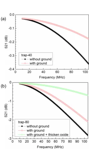
on SiO2 layer thickness. Fig. 12 (a) and (b) shows the simulated insertion losses (S21) for
trap-40 and trap-80 type without and with ground plane. For both trap types, the insertion losses
are reduced by adding the ground plane. The lower insertion loss correlates to lower
capacitance, higher Q factor and better resonance performance of the trap.
The ground plane can be an effective shielding layer to prevent power dissipation to Si
substrate. However, the improvement may still be limited for the trap with large electrode
area to have an insufficiently low RF loss, as reflected in the simulated S21 data. At a typical
resonance frequency of 40 MHz, the simulated S21 of trap-40 and trap-80 with the ground
plane are 0.05 MHz and 0.40 MHz, respectively. The larger loss of trap-80 is attributed to the
large electrode area of trap-80 compared to that of trap-40 (Table I). The large electrode area
results in a larger parasitic capacitance induced between the electrode and the ground layer.
A very thick SiO2 insulation layer is reported to effectively reduce such parasitic capacitance
[17]. By simulation, we found that by increasing the SiO2 thickness from 3 μm to 6 μm, S21
can be further improved to -0.13 dB at 40 MHz for trap-80. However, to fabricate a very thick
SiO2 layer poses challenge for large-scale wafer fabrication due to the large structural stress
induced by the thick SiO2 layer. Through-silicon-via (TSV) interconnect is proposed to
eliminate the wire-bonding pad of surface trap so to significantly reduce the electrode area
and bring the benefit of S21 improvement [18], which can be another method to improve RF
loss for large trap types such trap-80. By combining the methods of utilizing ground plane,
thickening the insulation layer and/or reducing electrode area by using TSV interconnect, the
surface trap based on Si substrate is expected to achieve the desired resonance performance,
which is perquisite for ion trapping experiment.
V. CONCLUSION
Large-scale fabrication of surface electrode ion trap on 300- mm Si wafer with novel Cu/Au
electroplated-electrodes is demonstrated using a Cu back end process. Cu/Au electrodes are
electroplated to replace the commonly used Au electrodes. Thin Au layer forms an effective
passivation layer to prevent Cu oxidation. SiO2 trenches are created in the electrode gap to
reduce the stray electric field. Process optimization is done to minimize the undercut in Cu/Au
electrodes which improves the leakage current between the fine-gap electrodes. Meshed
ground structure is fabricated using Cu single damascene process to improve the resonance
performance. The fabricated surface electrode ion trap shows promising electrical properties
with a comparably high Q factor and peak power to that of the reference capacitor, which is
requisite for ion trapping functionalities.
ACKNOWLEDGMENTS
We would like to acknowledge the Facility for Analysis, Characterization, Testing and
Simulation, Nanyang Technological University, Singapore, for use of their XPS facilities and Dr.
T. Salim for his XPS analysis. We greatly thank W.W. Seit, in Institute of Microelectronics,
Singapore for his technical supports on wire-bonding and packaging. We are grateful to
colleagues in VIRTUS, Nanyang Technological University, Singapore for their supports on RF
resonator test. The work was financially supported by A*STAR Quantum Technology for
Engineering (A1685b0005).
REFERENCES
[1] B. Lekitsch et al., “Blueprint for a microwave trapped ion quantum computer,” Sci. Adv.,
vol. 3, no. 2, 2017.
[2] C. Monroe and J. Kim, “Scaling the Ion Trap Quantum Processor,” Science (80-. )., vol.
339, no. 6124, pp. 1164–1169, 2013.
[3] E. Mount et al., “Single qubit manipulation in a microfabricated
surface electrode ion trap,” New J. Phys., vol. 15, no. 9, p. 93018,
Sep. 2013.
[4] T. P. Harty et al., “High-Fidelity Preparation, Gates, Memory, and
Readout of a Trapped-Ion Quantum Bit,” Phys. Rev. Lett., vol. 113,
no. 22, p. 220501, Nov. 2014.
[5] C. D. Bruzewicz, J. Chiaverini, R. McConnell, and J. M. Sage,
“Trapped-ion quantum computing: Progress and challenges,” Appl.
Phys. Rev., vol. 6, no. 2, 2019.
[6] J. Chiaverini et al., “Surface-Electrode Architecture for Ion-Trap
Quantum Information Processing,” vol. 5, no. 6, pp. 419–439, 2005.
[7] E. Mount et al., “Single qubit manipulation in a microfabricated
surface electrode ion trap,” New J. Phys., vol. 15, 2013.
[8] D. L. Moehring et al., “Design, fabrication and experimental demonstration of junction
surface ion traps,” New J. Phys., vol. 13,
2011.
[9] N. D. Guise et al., “Ball-grid array architecture for microfabricated
ion traps,” J. Appl. Phys., vol. 117, no. 17, 2015.
scalable, parallel, single-qubit operations in a surface-electrode ion
trap,” Appl. Phys. B Lasers Opt., vol. 114, no. 1–2, pp. 3–10, 2014.
[11] D. An et al., “Surface trap with dc-tunable ion-electrode distance,”
Rev. Sci. Instrum., vol. 89, no. 9, 2018.
[12] M. Harlander, M. Brownnutt, W. Hänsel, and R. Blatt, “Trapped-ion
probing of light-induced charging effects on dielectrics,” New J.
Phys., vol. 12, 2010.
[13] J. H. Wesenberg, “Electrostatics of surface-electrode ion traps,”
Phys. Rev. A, vol. 78, no. 6, pp. 1–12, 2008.
[14] J. Tao et al., “3D Integration of CMOS-Compatible Surface Electrode
Ion Trap and Silicon Photonics for Scalable Quantum Computing,” in 2019 IEEE 69th
Electronic Components and Technology Conference (ECTC), 2019, pp. 1735–1743.
[15] M. D. Hughes, B. Lekitsch, J. A. Broersma, and W. K. Hensinger, “Microfabricated Ion
Traps,” Contemp. Phys., vol. 52, no. 6, pp. 505– 529, 2011.
[16] K. Yoon et al., “Modeling and analysis of coupling between TSVs, metal, and RDL
interconnects in TSV-based 3D IC with silicon interposer,” Proc. Electron. Packag. Technol.
Conf. EPTC, vol. 3, pp. 702–706, 2009.
[17] S. C. Doret et al., “Controlling trapping potentials and stray electric fields in a
microfabricated ion trap through design and compensation,” New J. Phys., vol. 14, 2012.
[18] J. Tao et al., “Design Considerations and Fabrication Challenges of Surface Electrode Ion
Trap with TSV Integration,” presented at the The IEEE International 3D Systems Integration
Conference (3DIC), Sendai, Japan, Oct 8-10, 2019.
FIGURE CAPTIONS
Fig. 1. Finite element modeling of electric pseudopotential in a surface trap with RF line
width of 40 μm (a) Surface trap model in COMSOL, and (b) pseudopotential contour in
XZ-plane at Y=0. Trapping ion height is ~ 40 μm above trap surface. (Trapped 88Sr+ ion with 200
V applied RF amplitude and 2π × 56 MHz drive frequency)
Fig. 2 Trap electrodes fabrication: (a) Top overall, top magnified and tilted SEM images of
SiO2 pad pattern, and (b) Top overall microscopic, top magnified and tilted SEM images of
Cu/Au electrode pattern.
Fig. 3 Cross-sectional SEM images of trap electrodes: (a) a trap electrode with 4 layers and
(b) the inter-electrode gap area: gap 1, gap between Au electrodes; gap 2, gap between Cu
electrodes; gap 3, gap between SiO2 pads.
Fig. 4 Monoatomic Ar+ XPS core-level (Au 4f, Cu 2p) spectra of Cu, Au chemical states in pad
surface before and after total etching cycles.
Fig. 5. XPS depth profiling of Au/Cu-Au/Cu layers (a) involution of Au 4f doublets in terms of
etching time, (b) involution of Cu 2p doublets in terms of etching time and (c) the
concentration profiling of Cu 2p and Au 4f in terms of etching time and the Au-Cu interface
with Cu 2p and Au 4f overlapping area is marked accordingly.
Fig. 6. Design of ion trap with ground plane: (a) schematic cross-sectional view of trap
electrodes with Cu ground. (b) Layout of trap electrodes (green) and the ground plane
(orange).
Fig. 7 Optical images of Cu Ground plane, (a) Cu ground with mesh structure fabricated with
single damascene process, (b) SiO2 patterning on top of ground layer, (c) trap electrode
fabrication and (d) the overall view of trap-20 geometry with the underneath ground plane.
Fig. 8 SEM images of trap electrode with ground plane, (a) top view and (b) cross-sectional
view.
Fig. 9 Full-wafer leakage current mapping for ion trap with ground layer.
Fig. 10 Basic test setup of RF resonator test with ion trap.
Fig. 11 Resonance curve of ion traps with/without ground layer compared to a reference
capacitor.
Fig. 12 Simulated insertion loss of ion trap without and with ground plane for (a) trap-40 and
(b) trap-80. The further improvement of S21 for tap-80 by thicken insulation layer is also
displayed in (b).
FIGURES
Fig. 1a
Fig. 1b
Fig. 2
Fig. 3
> REPLACE THIS LINE WITH YOUR PAPER IDENTIFICATION NUMBER (DOUBLE-CLICK HERE TO EDIT) < 2
complexity and diversity requirement imposed on the surface trap design, the consideration to incorporate the trap fabrication into a more foundry compatible, large-volume and fast turn-over time production to prove the design concept becomes imperative.
In this work, we fabricate the surface trap using a main-stream 300-mm Si wafer in standard foundry conditions. The Cu backend process is employed to fabricate a thick and flat
trap electrodes. The SiO2 insulation layer between the
electrodes is dry etched to reduce the electrostatic charges induced stray fields. To address the parasitic coupling induced by Si substrate, a ground plane is designed and fabricated in the ion trap. The fabricated traps are then tested to examine their compliance with the required resonance performance for proper operation of the ion-trap.
II. SURFACE ELECTRODE FABRICATION
Surface electrode ion trap fabrication is accomplished on standard 300-mm Si wafer platform. Four trap types are included in one layout design. The traps are designed with similar geometries but different RF line widths and spaces, which result in different trapping ion heights. Table 1 lists the trap geometrical specifications with simulated ion heights for each trap types. For trap fabrication, two important process
steps are: (1) SiO2 insulation layer patterning and dry etch, and
(2) Cu/Au metal layer patterning and electroplating. Fig. 2 (a) shows the Scanning Electron Microscopy (SEM) images of the
patterned SiO2 pads with overall, magnified and titled view.
The insulation layer is formed by 3 µm thick low-stress
Plasma-enhanced chemical vapor deposition (PECVD)-deposited SiO2.
SiO2 in the electrode gap area is patterned and dry-etched to
reduce the effective exposed dielectric surface to the ion and the stray electric field around ion-trapping region [12]. Cu/Au electrode is subsequently aligned, patterned and electroplated
on top of SiO2 pad. Fig. 2 (b) shows the microscopic top
overview, SEM top magnified and titled images after the Cu/Au electrodes fabrication. The metal electrodes are recessed by 1
µm to the SiO2 pads. Au is directly deposited on Cu layer as
surface passivation layer to control the amount of Cu oxidation. The inter-diffusion of Au and Cu is studied by X-ray photoelectron spectroscopy (XPS) analysis which will be discussed in section B.
A. Cross-sectional Analysis
The cross-sectional SEM views of ion trap electrodes with four layers and the inter-electrode gap area are shown in Fig. 3 (a) and (b), respectively. The designed and measured dimensions of the electrode layer and gap are summarized in
Table II. The SiO2 layer thickness is optimized to be ~3 µm,
juggling between acceptable stress-level for full-wafer fabrication, and sufficient thickness to address the parasitic capacitance issue in Si substrate. Ti/Cu is deposited as the barrier layer and seed layer for Cu electroplating. A thick Cu layer of > 3 µm is electroplated to further hinder the ion sight to the exposed dielectric and also serves as an effective thermal dissipation layer to reduce the trap heating. To approximate the “gapless plane” trap geometry [13], the minimum
inter-Fig. 1. Finite element modeling of electric pseudopotential in a surface trap with RF line width of 40 µm (a) Surface trap model in COMSOL, and (b) pseudopotential contour in XZ-plane at Y=0. Trapping ion height is ~ 40 µm above trap surface. (Trapped 88Sr+ ion with 200 V applied RF amplitude and 2π × 56 MHz drive frequency) (b) X yz (a) Ion-trapping Point
Fig. 2 Trap electrodes fabrication: (a) Top overall, top magnified and tilted SEM images of SiO2 pad pattern, and (b) Top overall microscopic, top magnified and tilted SEM images of Cu/Au electrode pattern.
TABLEI
TRAP GEOMETRIES AND SIMULATED ION HEIGHTS
Trap Type RF line width (µm) RF line space (µm) Insulation Gap (µm) RF line length (µm) Electrode area (mm2) Simulated ion heights (µm) Trap-120 120 130/140 5/10 4380 54.47 110 Trap-80 80 90/100 5/10 2920 53.56 75 Trap-40 40 50/60 5/10 1460 12.40 40 Trap-20 20 30/40 5/10 730 2.61 20
> REPLACE THIS LINE WITH YOUR PAPER IDENTIFICATION NUMBER (DOUBLE-CLICK HERE TO EDIT) < 3
electrode gap in the trap center is kept at 5 µm. From Fig. 3(b), a slight undercut in Cu layer is observed due to the etching of Cu sidewalls during Cu seed wet etching process. Considering gap1 and gap2 in Fig. 3(b), a prominent Cu undercut to Au of 1.4 µm can be approximated. This generates the Au overhang structure which is mechanically unstable and may cause electrical bridging issue between the electrodes. Therefore, further process improvement is carried out to minimize the undercut width which will be discussed in the section III, B.
B. XPS Analysis of Au-Cu Electrode
A thin layer of Au is electroplated on top of base Cu as the surface finish layer to prevent Cu oxidation in atmospheric environment. Metal oxidation must be avoided on the electrode surface as it can induce unwanted charges and stray electric field, which will affect the ion trapping performance. To investigate the chemical states of the top surface metal and the interface composition of Cu-Au electrode, XPS technique is employed to study the layer information of Au/Au-Cu
interface/Cu by using 5 keV monoatomic Ar+ etching cycles to
etch a pad area of 1.5 mm × 1.5 mm for 54 cycles with an etching rate of 300 s/cycle.
Fig. 4 shows the XPS core-level spectra of Au 4f, Cu 2p on
the corresponding metal layer before and after the Ar+ etching
cycles. Au 4f and Cu 2p major peaks are chosen to fit the XPS models. Peak-fitting is done by considering the doublets as a pair constrained by the full-width half maximum and the intensity ratio, in order to extract information such as binding
energy and the area under the curve. From the spectra, Au 4f and Cu 2p are the main composition on the surface before and after etching. However, a small amount Cu species (< 3 at%,
Cu2+:Cu+ = 1.28:1.00) are detected on the initial surface, which
is not found on the surface after the first etching cycle. The presence of these Cu species can be attributed to environmentally-induced contaminations where Cu ions in the electroplating bath can be the sources of Cu traces on the Au surface.
On the other hand, the Au and Cu evolution in terms of etching time is plotted in Fig. 5 (a) and (b), respectively. In the
first ~6000s of etching time, Au doublets of 4f5/2 and 4f7/2 are
the main spectra peaks. As the etching continues, Cu doublets
of 2p1/2 and 2p2/3 gradually emerge to overtake the Au doublets
as the main spectra peaks. An initial energy drift of Au doublets to the higher binding energy is also observed in the first few cycles, which become relatively “stable” in the subsequent
Fig. 5. XPS depth profiling of Au/Cu-Au/Cu layers (a) involution of Au 4f doublets in terms of etching time, (b) involution of Cu 2p doublets in terms of etching time and (c) the concentration profiling of Cu 2p and Au 4f in terms of etching time and the Au-Cu interface with Cu 2p and Au 4f overlapping area is marked accordingly. Au 4f7/2 Au 4f5/2 Au 4f7/2 Au 4f5/2 Energy drift Cu 2p3/2 Cu 2p1/2 Cu 2p3/2 Cu 2p1/2 (a) (b) (c) Au-Cu interface
Fig. 4 Monoatomic Ar+ XPS core-level (Au 4f, Cu 2p) spectra of Cu, Au chemical states in pad surface before and after total etching cycles.
TABLEII
LAYER AND GAP DIMENSIONS OF TRAP ELECTRODES
Designed (µm) Measured (µm) SiO2 Thickness 3 3.1 SiO2 Gap 3 3.1 Ti Thickness 0.1 0.1 Cu Thickness 3 3.7 Cu Gap 5 6.6 Au Thickness 0.2 0.2 Au Gap 5 3.8 Cu undercut to Au NA 1.4
Fig. 3 Cross-sectional SEM images of trap electrodes: (a) a trap electrode with 4 layers and (b) the inter-electrode gap area: gap 1, gap between Au electrodes; gap 2, gap between Cu electrodes; gap 3, gap between SiO2 pads.
Fig. 4
Fig. 5
Fig. 6
> REPLACE THIS LINE WITH YOUR PAPER IDENTIFICATION NUMBER (DOUBLE-CLICK HERE TO EDIT) < 3
electrode gap in the trap center is kept at 5 µm. From Fig. 3(b), a slight undercut in Cu layer is observed due to the etching of Cu sidewalls during Cu seed wet etching process. Considering gap1 and gap2 in Fig. 3(b), a prominent Cu undercut to Au of 1.4 µm can be approximated. This generates the Au overhang structure which is mechanically unstable and may cause electrical bridging issue between the electrodes. Therefore, further process improvement is carried out to minimize the undercut width which will be discussed in the section III, B.
B. XPS Analysis of Au-Cu Electrode
A thin layer of Au is electroplated on top of base Cu as the surface finish layer to prevent Cu oxidation in atmospheric environment. Metal oxidation must be avoided on the electrode surface as it can induce unwanted charges and stray electric field, which will affect the ion trapping performance. To investigate the chemical states of the top surface metal and the interface composition of Cu-Au electrode, XPS technique is employed to study the layer information of Au/Au-Cu
interface/Cu by using 5 keV monoatomic Ar+ etching cycles to
etch a pad area of 1.5 mm × 1.5 mm for 54 cycles with an etching rate of 300 s/cycle.
Fig. 4 shows the XPS core-level spectra of Au 4f, Cu 2p on
the corresponding metal layer before and after the Ar+ etching
cycles. Au 4f and Cu 2p major peaks are chosen to fit the XPS models. Peak-fitting is done by considering the doublets as a pair constrained by the full-width half maximum and the intensity ratio, in order to extract information such as binding
energy and the area under the curve. From the spectra, Au 4f and Cu 2p are the main composition on the surface before and after etching. However, a small amount Cu species (< 3 at%,
Cu2+:Cu+ = 1.28:1.00) are detected on the initial surface, which
is not found on the surface after the first etching cycle. The presence of these Cu species can be attributed to environmentally-induced contaminations where Cu ions in the electroplating bath can be the sources of Cu traces on the Au surface.
On the other hand, the Au and Cu evolution in terms of etching time is plotted in Fig. 5 (a) and (b), respectively. In the
first ~6000s of etching time, Au doublets of 4f5/2 and 4f7/2 are
the main spectra peaks. As the etching continues, Cu doublets
of 2p1/2 and 2p2/3 gradually emerge to overtake the Au doublets
as the main spectra peaks. An initial energy drift of Au doublets to the higher binding energy is also observed in the first few cycles, which become relatively “stable” in the subsequent
Fig. 5. XPS depth profiling of Au/Cu-Au/Cu layers (a) involution of Au 4f doublets in terms of etching time, (b) involution of Cu 2p doublets in terms of etching time and (c) the concentration profiling of Cu 2p and Au 4f in terms of etching time and the Au-Cu interface with Cu 2p and Au 4f overlapping area is marked accordingly. Au 4f7/2 Au 4f5/2 Au 4f7/2 Au 4f5/2 Energy drift Cu 2p3/2 Cu 2p1/2 Cu 2p3/2 Cu 2p1/2 (a) (b) (c) Au-Cu interface
Fig. 4 Monoatomic Ar+ XPS core-level (Au 4f, Cu 2p) spectra of Cu, Au chemical states in pad surface before and after total etching cycles.
TABLEII
LAYER AND GAP DIMENSIONS OF TRAP ELECTRODES
Designed (µm) Measured (µm) SiO2 Thickness 3 3.1 SiO2 Gap 3 3.1 Ti Thickness 0.1 0.1 Cu Thickness 3 3.7 Cu Gap 5 6.6 Au Thickness 0.2 0.2 Au Gap 5 3.8 Cu undercut to Au NA 1.4
Fig. 3 Cross-sectional SEM images of trap electrodes: (a) a trap electrode with 4 layers and (b) the inter-electrode gap area: gap 1, gap between Au electrodes; gap 2, gap between Cu electrodes; gap 3, gap between SiO2 pads.
> REPLACE THIS LINE WITH YOUR PAPER IDENTIFICATION NUMBER (DOUBLE-CLICK HERE TO EDIT) < 4
cycles. The energy drift is not detected on the Cu doublets. In Fig. 5 (c), the concentration of Au and Cu elements is calculated by relying on relative sensitivity factor (RSF) values and the area under the curves for the peaks. The Au-Cu overlapping in the etching period of ~6000 s to ~10000 s is marked as Cu-Au interface. The inter-diffusion of Cu and Au is noticeable in the interface area with a 5-order of magnitude change in the ratio between Au and Cu. From the plot, it can be estimated that the distance between the Cu-Au interface area and the top Au surface is about 1.5 times of the distance of the whole interface area, which is considered as a sufficiently thick layer to prevent Cu diffusion onto Au surface.
III. TRAP WITH GROUND PLANE
The design of ground plane underneath the ion trap electrodes is shown in Fig. 6. The ground plane is inserted between the Si substrate and the SiO2 layer to shield the
Si-induced RF loss. We designed the mesh ground structure on non-RF area to facilitate large area metal fabrication and used the ground plate (no mesh) in the central RF line area as shown in Fig. 6 (b). A bond pad is designed on top left corner of ground layer for wire connection purpose. It should be noted that the ground layer can further reduce the exposed dielectric surface in inter-electrode gap area and therefore minimizing the stray field effect.
A. Cu Ground Fabrication
Cu single damascene process is used to fabricate the ground
plane. First, SiO2 layer of 2 µm thick is deposited by PECVD
on a 300-mm, p-doped, high-resistivity Si wafer (resistivity > 750 Ω·cm). The mesh structure of 15 µm wide strips with 15 µm separation in both X and Y direction is patterned and etched for Cu filling. The mesh structure is designed to meet the metal density constrains for effective chemical-mechanical polishing (CMP) steps. The fabricated Cu ground after CMP is shown in
Fig. 7 (a). The insulating SiO2 layer of trap electrodes are then
deposited and patterned on top of the ground layer as shown in
Fig. 7 (b). Finally, the electroplated Cu/Au electrodes are
formed on SiO2 pads as shown in Fig. 7 (c). The overall view
of a trap geometry with underneath ground plane is shown in Fig. 7 (d).
B. Reduced Cu Undercut
As mentioned earlier, Cu undercut and overhanging Au may cause electrical bridging between the electrodes, which exert devastating effects on the functionality of the ion trap. Process optimization is conducted by adjusting the Cu seed etching time. By fully opening the seed layer while minimizing the wet etching time, the undercut of Cu to Au layer is significantly reduced to ~ 0.2 µm, as shown in Fig. 8. Fig. 8 (a) shows the top view SEM images of trap electrode on the ground plane. Fig. 8 (b) shows the cross-sectional image comprising the different layers of electrode, insulation and ground. It can be seen from the image that some voiding area of Cu ground layer under the edge of SiO2 pad exists due to seed layer etching
process. However, the continuity of the ground layer is not compromised due to the minimized etching time and the sufficiently thick Cu layer. The designed and measured dimensions of layer thickness and inter-electrode distances are given in Table III. To incorporate ground electrode in the ion
trap, three more layers are added in this fabrication as SiO2 layer
under Cu ground, Cu ground layer and Si3N4 layer using
well-established foundry processes. By optimizing the Cu undercut,
Fig. 6. Design of ion trap with ground plane: (a) schematic cross-sectional view of trap electrodes with Cu ground. (b) Layout of trap electrodes (green) and the ground plane (orange).
Si
SiO2 Cu ground Meshed ground
Si3N4 SiO2 Cu Au DC RF DC RF DC Ti (a) Meshed ground Central ground plate Bonding pad
(b)
Fig. 7 Optical images of Cu Ground plane, (a) Cu ground with mesh structure fabricated with single damascene process, (b) SiO2 patterning on top of ground layer, (c) trap electrode fabrication and (d) the overall view of trap-20 geometry with the underneath ground plane.
(a) (b) (c) (d) Cu bond pad Cu mesh SiO2 Au 100 µm 100 µm 500 µm 100 µm
Fig. 8 SEM images of trap electrode with ground plane, (a) top view and (b) cross-sectional view. Cu (ground) SiO2 Cu (electrode) Ti SiO2 Si3N4 Au 5 µm 80 µm (a) (b) 7.743 µm 3.525 µm 3.282 µm 3. 081 µm 3. 059 µm 0. 879 µm 0.867 µm
Fig. 7
Fig. 8
Fig. 9
Fig. 10
> REPLACE THIS LINE WITH YOUR PAPER IDENTIFICATION NUMBER (DOUBLE-CLICK HERE TO EDIT) < 4
cycles. The energy drift is not detected on the Cu doublets. In Fig. 5 (c), the concentration of Au and Cu elements is calculated by relying on relative sensitivity factor (RSF) values and the area under the curves for the peaks. The Au-Cu overlapping in the etching period of ~6000 s to ~10000 s is marked as Cu-Au interface. The inter-diffusion of Cu and Au is noticeable in the interface area with a 5-order of magnitude change in the ratio between Au and Cu. From the plot, it can be estimated that the distance between the Cu-Au interface area and the top Au surface is about 1.5 times of the distance of the whole interface area, which is considered as a sufficiently thick layer to prevent Cu diffusion onto Au surface.
III. TRAP WITH GROUND PLANE
The design of ground plane underneath the ion trap electrodes is shown in Fig. 6. The ground plane is inserted between the Si substrate and the SiO2 layer to shield the
Si-induced RF loss. We designed the mesh ground structure on non-RF area to facilitate large area metal fabrication and used the ground plate (no mesh) in the central RF line area as shown in Fig. 6 (b). A bond pad is designed on top left corner of ground layer for wire connection purpose. It should be noted that the ground layer can further reduce the exposed dielectric surface in inter-electrode gap area and therefore minimizing the stray field effect.
A. Cu Ground Fabrication
Cu single damascene process is used to fabricate the ground
plane. First, SiO2 layer of 2 µm thick is deposited by PECVD
on a 300-mm, p-doped, high-resistivity Si wafer (resistivity > 750 Ω·cm). The mesh structure of 15 µm wide strips with 15 µm separation in both X and Y direction is patterned and etched for Cu filling. The mesh structure is designed to meet the metal density constrains for effective chemical-mechanical polishing (CMP) steps. The fabricated Cu ground after CMP is shown in
Fig. 7 (a). The insulating SiO2 layer of trap electrodes are then
deposited and patterned on top of the ground layer as shown in
Fig. 7 (b). Finally, the electroplated Cu/Au electrodes are
formed on SiO2 pads as shown in Fig. 7 (c). The overall view
of a trap geometry with underneath ground plane is shown in Fig. 7 (d).
B. Reduced Cu Undercut
As mentioned earlier, Cu undercut and overhanging Au may cause electrical bridging between the electrodes, which exert devastating effects on the functionality of the ion trap. Process optimization is conducted by adjusting the Cu seed etching time. By fully opening the seed layer while minimizing the wet etching time, the undercut of Cu to Au layer is significantly reduced to ~ 0.2 µm, as shown in Fig. 8. Fig. 8 (a) shows the top view SEM images of trap electrode on the ground plane. Fig. 8 (b) shows the cross-sectional image comprising the different layers of electrode, insulation and ground. It can be seen from the image that some voiding area of Cu ground layer under the edge of SiO2 pad exists due to seed layer etching
process. However, the continuity of the ground layer is not compromised due to the minimized etching time and the sufficiently thick Cu layer. The designed and measured dimensions of layer thickness and inter-electrode distances are given in Table III. To incorporate ground electrode in the ion
trap, three more layers are added in this fabrication as SiO2 layer
under Cu ground, Cu ground layer and Si3N4 layer using
well-established foundry processes. By optimizing the Cu undercut,
Fig. 6. Design of ion trap with ground plane: (a) schematic cross-sectional view of trap electrodes with Cu ground. (b) Layout of trap electrodes (green) and the ground plane (orange).
Si
SiO2 Cu ground Meshed ground
Si3N4 SiO2 Cu Au DC RF DC RF DC Ti (a) Meshed ground Central ground plate Bonding pad
(b)
Fig. 7 Optical images of Cu Ground plane, (a) Cu ground with mesh structure fabricated with single damascene process, (b) SiO2 patterning on top of ground layer, (c) trap electrode fabrication and (d) the overall view of trap-20 geometry with the underneath ground plane.
(a) (b) (c) (d) Cu bond pad Cu mesh SiO2 Au 100 µm 100 µm 500 µm 100 µm
Fig. 8 SEM images of trap electrode with ground plane, (a) top view and (b) cross-sectional view. Cu (ground) SiO2 Cu (electrode) Ti SiO2 Si3N4 Au 5 µm 80 µm (a) (b) 7.743 µm 3.525 µm 3.282 µm 3. 081 µm 3. 059 µm 0. 879 µm 0.867 µm
> REPLACE THIS LINE WITH YOUR PAPER IDENTIFICATION NUMBER (DOUBLE-CLICK HERE TO EDIT) < 5
the leakage current performance of the trap die across the wafer is clearly improved. The full-wafer leakage current mapping is given in Fig. 9 and the good die percentage of the leakage
current < 10-7 A is significantly increased to > 90%, compared
to previously reported ~70% [14] for the same trap type.
IV. RFRESONATOR TEST
RF resonator test is conducted to evaluate the required resonance performance of the fabricated traps to realizing ion trapping. The trap is connected as a capacitor to an external inductor to form a series connected LCR resonator circuit to step up the input voltage to the required RF trapping voltage (~200 V). To form the resonator circuit, the trap is packaged in the ceramic pin gird array (CPGA) package and connected to a toroidal inductor which is contained in a metal shielding box. An input RF power of -10 dBm is supplied by a signal generator. A set of capacitor dividers C1 and C2 (with C1:C2 = 1:20) is connected to the inductor and a signal analyzer for suppressed power readout. To generate the resonance curve, a linear frequency sweep is conducted from 10 to 100 MHz with a step size of 1 MHz. The resonance curve is compared to a reference curve generated by a standard capacitor of 3.3 pF to address the required resonance performance. Fig. 10 shows the basic experiment setup of RF resonator test with ion trap.
A. Resonance Performance
Two types of traps, with RF line widths of 40 and 80 µm (denoted as trap-40 and trap-80, in Table I), respectively, without and with ground plane, are tested. The resonance curves
are shown in Fig. 11. The resonance frequency, f0, and the
quality, Q factor (i.e. the sharpness of the curve), can be obtained from the curves by the peak power frequency and 3 dB bandwidth. The reference curve generated by 3.3 pF standard capacitor is also included in the plot for comparison. The resonance results are given in Table IV. By comparing the same type of traps without and with the ground plane, we see significant Q factor increase of 2 and 6 for trap-40 and trap-80, respectively. The Q factor values are close to the reference Q-factor of 18.5 generated by the capacitor. Q Q-factor is one of the key parameters in the resonator circuit, because it is proportional to voltage gain on the trap electrodes and reversely proportional to the power dissipation in the substrate [15]. With the higher Q factor, the peak power of the traps with the ground plane also increase 13 and 11 dBm for the trap-40 and trap-80, respectively. However, the power peak of trap-80 is still low compared to that of reference capacitor. This can be caused due to: 1) large electrode surface area of 80 compared to trap-40 and 2) the limitation of ground shield effect for large electrode area to obtain required RF loss improvement, which will be discussed in next section.
Fig. 11 Resonance curve of ion traps with/without ground layer compared to a reference capacitor.
Fig. 9 Full-wafer leakage current mapping for ion trap with ground layer.
Slot ID: 9
9.77E-10 7.73E-10 7.11E-10 6.43E-10 6.75E-10
1.10E-09 8.03E-10 8.45E-10 9.14E-10 7.65E-10 6.91E-10 7.43E-10 6.95E-10 6.26E-10 8.97E-10 8.61E-10 8.78E-10 8.87E-10 8.92E-10 9.24E-10 8.52E-10 7.50E-10 8.54E-10 5.88E-10 5.88E-10 5.03E-07 1.01E-09 8.60E-10 9.20E-10 1.11E-09 1.20E-09 1.06E-09 1.06E-08 8.43E-10 1.04E-09 9.29E-10 5.65E-10 6.52E-10 1.47E-06 9.66E-10 7.83E-10 9.78E-10 1.04E-09 7.97E-10 1.04E-09 6.31E-10 8.60E-10 6.92E-10 7.11E-10 5.21E-10 5.90E-10 6.56E-10 8.16E-10 8.11E-10 8.16E-10 6.83E-10 1.03E-09 2.77E-08 1.64E-07 8.53E-10 9.84E-10 8.53E-10 8.49E-10 6.18E-10 5.65E-08 1.03E-09 9.27E-10 1.05E-09 1.07E-09 1.35E-09 1.22E-09 1.05E-09 1.23E-09 1.09E-09 8.91E-10 1.87E-07 1.01E-07
4.78E-06 1.08E-09 9.36E-08 1.12E-09 1.10E-07 9.56E-10 7.39E-10 9.23E-10 7.28E-10 6.58E-10 3.06E-09 4.09E-06 1.67E-09 9.89E-10 1.19E-09 1.18E-09 6.54E-10 9.99E-10 9.52E-10 1.34E-09
3.05E-09 5.06E-08 1.24E-09 1.12E-05 6.95E-10 <1E-7
<1E-6 >1E-7 >1E-6
TABLEIII
LAYER AND GAP DIMENSIONS OF TRAP ELECTRODES WITH GROUND LAYER
Designed (µm) Measured (µm)
SiO2 thickness underneath
Cu ground 1 0.9 Cu ground thickness 1 0.9 Si3N4 thickness 0.1 0.1 SiO2 Thickness 3 3.1 SiO2 Gap 3 3.3 Ti Thickness 0.1 0.1 Cu electrode Thickness 3 3.1 Cu Gap 5 7.7 Au Thickness 0.2 0.2 Au Gap 5 7.3 Cu undercut to Au NA 0.2
Fig. 10 Basic test setup of RF resonator test with ion trap.
Signal Generator Signal Analyzer
Toroidal inductor
C1 C2
Trap in Package
> REPLACE THIS LINE WITH YOUR PAPER IDENTIFICATION NUMBER (DOUBLE-CLICK HERE TO EDIT) < 5
the leakage current performance of the trap die across the wafer is clearly improved. The full-wafer leakage current mapping is given in Fig. 9 and the good die percentage of the leakage
current < 10-7 A is significantly increased to > 90%, compared
to previously reported ~70% [14] for the same trap type.
IV. RFRESONATOR TEST
RF resonator test is conducted to evaluate the required resonance performance of the fabricated traps to realizing ion trapping. The trap is connected as a capacitor to an external inductor to form a series connected LCR resonator circuit to step up the input voltage to the required RF trapping voltage (~200 V). To form the resonator circuit, the trap is packaged in the ceramic pin gird array (CPGA) package and connected to a toroidal inductor which is contained in a metal shielding box. An input RF power of -10 dBm is supplied by a signal generator. A set of capacitor dividers C1 and C2 (with C1:C2 = 1:20) is connected to the inductor and a signal analyzer for suppressed power readout. To generate the resonance curve, a linear frequency sweep is conducted from 10 to 100 MHz with a step size of 1 MHz. The resonance curve is compared to a reference curve generated by a standard capacitor of 3.3 pF to address the required resonance performance. Fig. 10 shows the basic experiment setup of RF resonator test with ion trap.
A. Resonance Performance
Two types of traps, with RF line widths of 40 and 80 µm (denoted as trap-40 and trap-80, in Table I), respectively, without and with ground plane, are tested. The resonance curves
are shown in Fig. 11. The resonance frequency, f0, and the
quality, Q factor (i.e. the sharpness of the curve), can be obtained from the curves by the peak power frequency and 3 dB bandwidth. The reference curve generated by 3.3 pF standard capacitor is also included in the plot for comparison. The resonance results are given in Table IV. By comparing the same type of traps without and with the ground plane, we see significant Q factor increase of 2 and 6 for trap-40 and trap-80, respectively. The Q factor values are close to the reference Q-factor of 18.5 generated by the capacitor. Q Q-factor is one of the key parameters in the resonator circuit, because it is proportional to voltage gain on the trap electrodes and reversely proportional to the power dissipation in the substrate [15]. With the higher Q factor, the peak power of the traps with the ground plane also increase 13 and 11 dBm for the trap-40 and trap-80, respectively. However, the power peak of trap-80 is still low compared to that of reference capacitor. This can be caused due to: 1) large electrode surface area of 80 compared to trap-40 and 2) the limitation of ground shield effect for large electrode area to obtain required RF loss improvement, which will be discussed in next section.
Fig. 11 Resonance curve of ion traps with/without ground layer compared to a reference capacitor.
Fig. 9 Full-wafer leakage current mapping for ion trap with ground layer.
Slot ID: 9
9.77E-10 7.73E-10 7.11E-10 6.43E-10 6.75E-10
1.10E-09 8.03E-10 8.45E-10 9.14E-10 7.65E-10 6.91E-10 7.43E-10 6.95E-10 6.26E-10 8.97E-10 8.61E-10 8.78E-10 8.87E-10 8.92E-10 9.24E-10 8.52E-10 7.50E-10 8.54E-10 5.88E-10 5.88E-10 5.03E-07 1.01E-09 8.60E-10 9.20E-10 1.11E-09 1.20E-09 1.06E-09 1.06E-08 8.43E-10 1.04E-09 9.29E-10 5.65E-10 6.52E-10 1.47E-06 9.66E-10 7.83E-10 9.78E-10 1.04E-09 7.97E-10 1.04E-09 6.31E-10 8.60E-10 6.92E-10 7.11E-10 5.21E-10 5.90E-10 6.56E-10 8.16E-10 8.11E-10 8.16E-10 6.83E-10 1.03E-09 2.77E-08 1.64E-07 8.53E-10 9.84E-10 8.53E-10 8.49E-10 6.18E-10 5.65E-08 1.03E-09 9.27E-10 1.05E-09 1.07E-09 1.35E-09 1.22E-09 1.05E-09 1.23E-09 1.09E-09 8.91E-10 1.87E-07 1.01E-07
4.78E-06 1.08E-09 9.36E-08 1.12E-09 1.10E-07 9.56E-10 7.39E-10 9.23E-10 7.28E-10 6.58E-10 3.06E-09 4.09E-06 1.67E-09 9.89E-10 1.19E-09 1.18E-09 6.54E-10 9.99E-10 9.52E-10 1.34E-09
3.05E-09 5.06E-08 1.24E-09 1.12E-05 6.95E-10 <1E-7
<1E-6 >1E-7 >1E-6
TABLEIII
LAYER AND GAP DIMENSIONS OF TRAP ELECTRODES WITH GROUND LAYER
Designed (µm) Measured (µm)
SiO2 thickness underneath
Cu ground 1 0.9 Cu ground thickness 1 0.9 Si3N4 thickness 0.1 0.1 SiO2 Thickness 3 3.1 SiO2 Gap 3 3.3 Ti Thickness 0.1 0.1 Cu electrode Thickness 3 3.1 Cu Gap 5 7.7 Au Thickness 0.2 0.2 Au Gap 5 7.3 Cu undercut to Au NA 0.2
Fig. 10 Basic test setup of RF resonator test with ion trap.
Signal Generator Signal Analyzer
Toroidal inductor
C1 C2