HAL Id: hal-00019208
https://hal.archives-ouvertes.fr/hal-00019208
Submitted on 17 Feb 2006
HAL is a multi-disciplinary open access
archive for the deposit and dissemination of
sci-entific research documents, whether they are
pub-lished or not. The documents may come from
teaching and research institutions in France or
abroad, or from public or private research centers.
L’archive ouverte pluridisciplinaire HAL, est
destinée au dépôt et à la diffusion de documents
scientifiques de niveau recherche, publiés ou non,
émanant des établissements d’enseignement et de
recherche français ou étrangers, des laboratoires
publics ou privés.
Cascade Lasers at Lambda=9 µm
Clément Faugeras, Sébastien Forget, Elizabeth Boer-Duchemin, Hideaki Page,
Jean-Yves Bengloan, Olivier Parillaud, Michel Calligaro, Carlo Sirtori,
Marcella Giovannini, Jérôme Faist
To cite this version:
Clément Faugeras, Sébastien Forget, Elizabeth Boer-Duchemin, Hideaki Page, Jean-Yves Bengloan,
et al.. High Power Room Temperature Emission Quantum Cascade Lasers at Lambda=9 µm. IEEE
Journal of Quantum Electronics, Institute of Electrical and Electronics Engineers, 2006, 41, pp.1430.
�10.1109/JQE.2005.858797�. �hal-00019208�
ccsd-00019208, version 1 - 17 Feb 2006
1 1 2 3 4High Power Room Temperature Emission Quantum
Cascade Lasers at
λ = 9µm
Cl´ement Faugeras, S´ebastien Forget, Elizabeth Boer-Duchemin, Hideaki Page, Jean-Yves Bengloan,
Olivier Parillaud, Michel Calligaro, Carlo Sirtori, Member IEEE, Marcella Giovannini and
J´erˆome Faist, Member IEEE
Abstract— We present two different techniques for processing
InP-based λ = 9µm quantum cascade lasers which improve the thermal dissipation in the device. The first process is based on hydrogen implantation creating an insulating layer to inject current selectively in one part of the active region. The second process uses a thick electroplated gold layer on the laser ridge to efficiently remove the heat produced in the active region. Each process is designed to improve heat evacuation leading to higher performances of the lasers and will be compared to a standard ridge structure from the same wafer. We give evidence that the process of proton implantation, efficient in GaAs based structures, is not directly applicable to InP based devices and we present a detailed analysis of the thermal properties of devices with an electroplated gold thick layer. With these lasers, an average power of 174 mW at a duty cycle of 40% has been measured at 10◦C.
Index Terms— quantum cascade laser, high power emission,
InP based device
I. INTRODUCTION
T
HE performance of quantum cascade lasers (QCL) [1] is continually improving [2], [3]. These unipolar devices emitting in the mid-infrared have great potential for applica-tions such as chemical sensing and free-space communicaapplica-tions [4], [5]. These applications will benefit greatly from room temperature, high power, continuous wave (CW) sources, and so, much of current QCL research is working towards this goal.The main difficulty on the route to high power and CW operation at room temperature is the large amount of heat that must be dissipated in the device. Typical operating voltages for InP-based QCLs are 7-10 V and threshold currents may be of the order of 1 A at room temperature. If we now consider that the best wall-plug efficiencies reported are of the order of a few percents, almost all the injected electrical power is converted into heat in the device. This means that about 10 W of power must be dissipated to prevent the active region from heating, which would lower the quantum efficiency and could block CW operation. In standard processed lasers, the Manuscript received February 17, 2006; revised February 17, 2006. this work is partially supported by EU FP6 Grant No. STRP 505642 ”ANSWER”. C. Faugeras, S. Forget and C. Sirtori are with P ˆole Mat´eriaux et Ph´enom`enes Quantiques, Universit´e Paris VII, 2 place Jussieu 75251 Paris, France.
E. Boer-Duchemin, H. Page, J.-Y. Bengloan, O. Parillaud and M. Calligaro are with Thales Research and Technology, Domaine de Corbeville, 91404 Orsay, France
M. Giovannini and J. Faist are with Institute of Physics, University of Neuchˆatel, Rue A. L. Breguet 1 2000 Neuchˆatel, Switzerland.
ridge is surrounded by a thin insulating layer (typically SiO2
or Si3N4), and then by a thin metallic contact layer, leading to
poor evacuation of the heat generated inside the active region. The most common answer to this challenge has been the realization of buried heterostructures (BH) [3], [6]. In these lasers, the active region is surrounded by semiconductor material with high thermal conductivity (unlike the case of standard ridge waveguide) so that heat may be easily dissipated in all directions. A drawback of BH lasers, however, is the extra regrowth step that is necessary. Recently, two alternatives have been proposed. They combine the simplicity of the standard ridge waveguide with the superior heat dissipation characteristics of the buried heterostructure. These techniques are the selective current injection technique [2], [7] and the use of a thick electroplated gold layer [8], [9]. We have applied both concepts to the same initial wafer to compare the performance obtained with the same active region but with different processing designs. In terms of emitted power, the best result reported so far atλ = 9µm [10] is an emission of
150 mW measured at room temperature at 6% of duty cycle. In this paper, we will see how the two techniques we have applied lead to equivalent and even higher performance with better thermal properties.
The paper is structured as follows. Section II gives a description of the structure of the laser. In Section III, we compare results obtained on standard processed lasers to results obtained on implanted lasers to illustrate the selective current injection technique in InP-based lasers. Section IV presents the results obtained on a third set of lasers, which have been covered with a thick electroplated gold layer to optimize heat evacuation. We discuss in Section V the thermal behavior of the lasers with the thick gold layer and we describe how to determine the thermal resistance of the device. We then present our conclusions.
II. LASER STRUCTURE
The active region of the devices is based on a four quantum well double phonon resonance design [6], [11]. The band diagram of this structure is shown in Fig. 1 with an applied electric field of 40 kV/cm. A period of the active region is
composed of four quantum wells, one narrow quantum well/ narrow injection barrier ensuring efficient injection into the upper state level (level 1 in Fig. 1) and three larger quantum wells creating three electronic levels with an energy separation equal to the optical phonon energy (36 meV). The laser
3 Minigap Miniband 1 2 3 4 Electron injection Electron extraction Miniband Minigap
Fig. 1. Schematic of the conduction band diagram of one period of the
4 quantum well active region together with the moduli-squared relevant wave functions. The laser transition involves levels 1 and 2 while the energy separation between levels 2 and 3 and between levels 3 and 4 is equal to a optical phonon energy. From the injection barrier, the layer sequence in nm is (bold layers are InAlAs and InGaAs layers are in roman)
4.0/1.9/0.7/5.8/0.9/5.7/0.9/5.0/2.2/3.4/1.4/3.3/1.3/3.2/1.5/
3.1/1.9/3.0/2.3/2.9/2.5/2.9.
transition involves levels 1 and 2 in Fig. 1. Together with the bound to continuum [12] active region, this structure has proved to be one of today’s best mid-infrared active region designs, allowing rapid electron escape from the lower level of the optical transition to achieve the population inversion necessary for laser emission. The 35 period lattice matched InGaAs/InAlAs well and barrier layers were grown on a doped InP substrate (100 µm) by molecular beam epitaxy (MBE)
while metalorganic vapor-phase epitaxy (MOVPE) was used to grow the top 3.3 µm InP cladding.
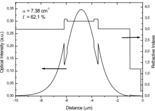
The calculated one dimensional refractive index and the optical intensity of this laser structure are presented in Fig. 2. On both sides of the 35 period active region, the waveguide is composed of 300 nm and 240 nm thick GaInAs layers that enhance the average refractive index difference between the core and the cladding regions of the waveguide. This results in a calculated overlap factor as high as 62.1 % and optical losses of 7.38 cm−1.
Initially, QCLs were developed in the GaInAs/AlInAs ma-terial system, grown on an InP substrate [13]. The choice of InP as a substrate for high power emission is appealing. Its advantages are numerous and include: 1) a low refractive index ensuring high optical overlap factors, 2) a high electrical conductivity making heavily doped (and thus lossy) layers unnecessary, and 3) a high thermal conductivity ensuring en-hanced heat evacuation with respect to other material systems [1].
III. SELECTIVE CURRENT INJECTION
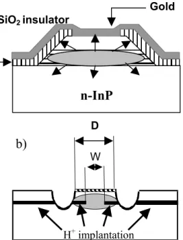
In this section, we will present and compare results obtained on two different types of samples. For the first set of lasers, called standard processed samples, wet chemical etching was used to define the ridge. A SiO2 dielectric layer was used
to electrically insulate the sides of the device from the top contact, as is shown in Fig. 3 a). The ridge width was 24µm
and the laser cavity lengths were 1 or 2 mm. For the 2 mm
-10 -8 -6 -4 -2 0 0,00 0,05 0,10 0,15 0,20 0,25 0,30 0,35 O p tic a l I n te n si ty ( a .u .) Distance (µm) 0,0 0,5 1,0 1,5 2,0 2,5 3,0 3,5 4,0 R e fr a ct iv e I n d e xe α = 7.38 cm-1 Γ = 62.1 %
Fig. 2. Calculated refractive index and mode profile of the laser waveguide
atλ=10µm. The overlap between the electric field and the laser active region
is Γ = 62.1 % and the calculated losses areα = 7.38 cm−1.
lasers, both front and back facets were cleaved thus resulting in a reflectivity of ∼ 23% [14], [15], while the back facet of the 1 mm samples was coated with a high reflectivity (HR) mirror (100 nm Al2O3/2 nm Ti/100 nm Au/100 nm Al2O3)
resulting in a reflectivity of ∼ 95 % at λ = 9 µm [14]. The samples were mounted epi-layer up in order to avoid any short circuits due to overflowing of the In solder on the facets of the laser. Throughout this paper, this process design will be used as a reference to evaluate the performance of the two other process designs that will be presented.
Fig. 3 b) shows the structure of the second set of lasers, named implanted lasers. Deep etched trenches define a stan-dard ridge structure, which, due to the refractive index change, confine the optical mode of the laser (shown as a shaded ellipse). Proton (H+) implantation was used to produce a
semi-insulating layer which defines a narrow injection channel in the ridge. Using this method, the width W of the electrically pumped area of the device is reduced with respect to the ridge width D. Current is then selectively injected into the center of the ridge.
Typical implantation energies and doses were600 keV and 2 × 10¹⁴ ions/cm2 respectively. With these parameters, the
implanted layer is 6 µm under the surface with a width of
1.14µm. The implanted ions then lie mostly in and below the
active region. After the implantation process, deep trenches were formed by wet chemical etching, ensuring smooth walls and thus avoiding optical scattering. As it is demonstrated in Ref. [2] for the GaAs/AlGaAs material system, threshold current optimization occurs when the ratio W/D of the
electrically pumped width W to the ridge total width D ranges from 0.5 to 0.7. We then chose the following parameters for
the device, a ridge of D = 14µm, an injection width of W = 10µm with a laser length of 1 mm. Samples were
mounted epi-layer down on high quality copper bases that had been pre-evaporated with 3-5 µm of indium solder.
For all experiments, the emission was collected with a germanium lens (f/0.8) and focused onto the detector using a ZnSe lens (f/1). The collection efficiency of this system is estimated to be 60%. At room temperature a calibrated MCT
detector was used for pulse measurements and a thermopile for the average power measurements. All measurements are re-ported without any corrections due to the collection efficiency
a)
W
D
H
+implantation
b)
SiO
2insulator
n-InP
Gold
Fig. 3. Schematic of the device. a) Standard processing using aSiO2layer
(vertical hatched layer) for electrical isolation, the horizontal hatched region represents the active region. The metallic contact layer is represented by the dark grey layer. b) The laser ridge of width D is defined by two trenches etched through the active layer. The injection window of width W is defined
by semi-insulating layers created via H+ implantation. The shaded region
represents the laser mode.
or to the transmission of the lenses.
The results for the first set of samples, processed with a SiO2 insulating layer, with cavity of 1 mm and with a HR
mirror, are shown in Fig. 4. These reference samples were not optimized in terms of heat dissipation, and therefore, at high temperature, only pulsed measurements at a low duty cycle were possible. The pulse width used was 50 ns with
a 1 kHz repetition rate, yielding a duty cycle of 0.005%.
This low duty cycle value insures that the thermal properties (material and mounting) of the device do not influence the measured characteristics. In particular, it is possible in this regime to compare devices with different ridge width because optical losses are not increased as the width is bigger than the wavelength. The interaction between the optical mode and the walls of the ridge, covered with an insulator (SiO2
or Si3N4) which is very lossy at these frequencies, is then
minimized [16]. The active volume increases with the width of the ridge as does the injected power. This parameter will then influence the characteristic of the laser when thermal effects are considered. Fig. 4 shows peak optical power and voltage as a function of current for T= 240 − 320 K. At 300
K, the threshold current (IT h) is 0.68 A, corresponding to
a threshold current density (JT h) of 2.8 kA/cm2, the slope
efficiency dP/dI is 655 mW/A and the maximum peak power is ∼ 550 mW. The characteristic temperature T0is defined by
the empirical relation between the current threshold density and temperature as JT h = J0eT /T0. T0 was determined by
fitting an exponential to the evolution of the threshold current
0,0 0,2 0,4 0,6 0,8 1,0 1,2 1,4 1,6 1,8 2,0 2,2 0 2 4 6 8 10 320K 300K 280K 260K 240K V o lta g e ( V ) Current (A) 0,0 0,1 0,2 0,3 0,4 0,5 0,6 0,7 0,8 O p tic a l P o w e r ( W )
Fig. 4. Pulsed measurements of optical power and voltage as a function of
current for a sample realized using standard processing. At 300 K,IT h is
0.68 A,JT his 2.8 kA/cm2, dP/dI is 655 mW/A and maximum peak power
is ∼ 550 mW. The ridge width is 24µm, with a cavity length of 1mm, and the rear facet is HR coated.
0,0 0,1 0,2 0,3 0,4 0,5 0,6 0,7 0,8 0,9 1,0 0 2 4 6 8 10 V o lta g e ( V ) Current (A) 0,00 0,05 0,10 0,15 0,20 0,25 0,30 0,35 0,40 280 K 240 K 300 K 260 K 320 K O p tic a l P o w e r ( W )
Fig. 5. Pulsed measurements of optical power and voltage as a function of
current for a proton implanted sample. At 300 K,IT his 0.34 A, JT his 3.4
kA/cm2
, dP/dI is 620 mW/A and maximum peak power is ∼ 235 mW. The
ridge width is 14µm, W = 10µm with a cavity length of 1mm, and the
rear facet is HR coated.
density with temperature, yielding a value of 180 K. Wall-plug efficiency, defined as the ratio of the peak optical power to instantaneous electrical power, is of 3% at 300 K.
The advantages of the reduction of electrically pumped region (W/D < 1) are threefold. Compared to a ridge device,
the pumped region is decreased and this causes a slight decrease in the optical mode overlap with the electrically pumped region (< 20%) and a comparable increase in the
threshold current density JT h. However, because of the area
reduction, the threshold currentIT h decreases by an amount
proportional to the ratio W/D. The first advantage is thus
clear: by strongly decreasing the threshold current, the heat dissipated in the devices is similarly reduced. The second advantage is that there is now semiconductor material with a high heat transfer coefficient surrounding the pumped section of the active region, thus improving heat evacuation. The third advantage is that, by decoupling the electrical and the optical confinement, the fundamental optical mode is preferentially pumped, insuring single mode emission [16].
Pulsed measurements of optical power vs current and of voltage vs current of these devices at the same duty cycle as for the reference lasers, are shown in Fig. 5. At 300 K,
5 0,0 0,2 0,4 0,6 0,8 1,0 0,00 0,01 0,02 0,03 0,04 0,05 0,06 0,07 8,80 8,85 8,90 8,95 9,00 T = 293K In te n s it y ( A .U .) Wavelength (µm)
O
p
tic
a
l P
o
w
e
r
(W
)
Current (A)
T = 0°C T = 10°C T = 20°CFig. 6. Continuous wave optical power as a function of current for an
implanted laser (D = 14, W = 10, with a cavity length of 2mm and the
rear facet HR coated) on a Peltier cooler : T= 0, 10 and 20◦C. Maximum
power is 20 mW, current threshold densityJT h = 3.3kA/cm2 and slope
efficiency dP/dI = 110mW/A at 20◦C. Insert: Emission spectrum near
threshold at room temperature.
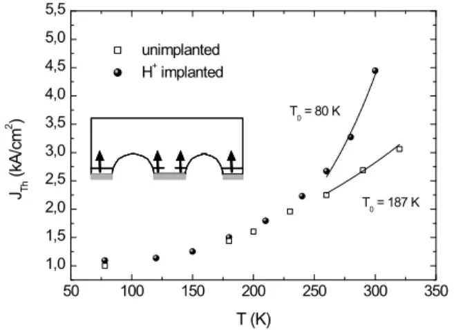
50 100 150 200 250 300 350 1,0 1,5 2,0 2,5 3,0 3,5 4,0 4,5 5,0 5,5 T0 = 187 K T0 = 80 K JTh ( kA /c m 2 ) T (K) unimplanted H+ implanted
Fig. 7. Threshold current in pulsed operation as a function of temperature
for a standard processed laser of 1 mm HR coated (open squares) and a proton implanted laser of 1 mm HR coated (black dots). The characteristic
T0 parameters are indicated. Inset: Schematic of the laser facet illustrating
the parasitic current channel (black arrows) at high temperatures owing to the breakdown of the implanted layer.
IT h= 0.34 A, JT h= 3.4 kA/cm2,dP/dI = 620 mW/A and
maximum peak power is ∼ 235 mW.
Samples processed using implantation operated continuous wave from liquid nitrogen to room temperature. Fig. 6 shows the optical power as a function of current for a typical implanted sample in CW operation on a Peltier cooler for T = 0, 10 and 20◦C. Maximum power at 20◦C was 20
mW, with values of 3.3 kA/cm2 and 110 mW/A for J T h
and dP/dI respectively. The inset of Fig. 6 shows the room temperature emission spectrum of this device measured with a high resolution (0.125 cm−1) FTIR Nicolet spectrometer.
The emission spectrum is centered at 8.91 µm. At 77 K, a
similar device but with cleaved facets in CW operation showed a threshold current density of 0.8 kA/cm2, a slope efficiency
of 475 mW/A with a maximum CW output power of 350 mW. The results presented in Fig. 6 for the implanted samples are comparable to those obtained from a buried heterostructure
device realized in the same material [6]. This is significant as it means that the simplified process of selective current injection produces devices with performances similar to BH devices. There is, however, a considerable discrepancy in the measured values of characteristic temperature T0(80 K for the
proton implanted sample and 187 K for the standard processed sample) as can be seen from the temperature dependance in pulsed mode of the threshold current for both processing presented in Fig. 7. As one can see, threshold current densities in the case of the implanted laser and for all temperatures below 240 K, are similar to those measured on standard processed lasers. At room temperature, the threshold current densities suddenly increase for the implanted sample, leading to a small value of the characteristic T0 parameter. This is
contrary to expectation, as the two devices should show the same temperature dependance as they are processed from the same material. This difference was not found in GaAs-based devices [2], and may be explained as follows.
While the process of proton implantation is very efficient for GaAs-based lasers [2], it breaks down at high temperatures for InP-based devices. Proton implantation in GaAs creates deep level centers which trap carriers, rendering the layer semi-insulating [17]. Since the defect states are near the middle of the band gap, the charge carriers remain trapped, even at elevated device operating temperatures, and the layers remain non-conducting. On the other hand, in n-InP, the created defects lead to the pinning of the Fermi level in the upper half of the band gap, thus allowing thermal activation of trapped carriers in the conduction band [18]. We explain the difference between the threshold values for implanted and non-implanted samples at room temperature by the thermally activated breakdown of the implantation layer. This causes a leakage current and a strong temperature dependance.
The breakdown of the insulating properties of the proton implanted layers at high temperatures in the ridge of the laser and also outside of the trenches (as shown in the inset in Fig. 7), can be clearly seen by comparing the I-V character-istics of the non-implanted and implanted samples shown in Fig. 4 and Fig. 5. For the implanted lasers, three effects are apparent while the temperature is varied: a flattening of the voltage knee, a general drop of the voltage and a shift toward higher currents of the negative differential resistance point. In this specific case, the electrical leaks are due to current flowing from the top contact to the substrate outside of the ridge of the laser.
To clarify this breakdown of the insulating properties of the implanted layer, we show in Fig. III the evolution of ln(Resistance) as a function of the inverse temperature measured in the region between two different lasers that is entirely implanted (see inset in Fig. III). Up to 200K, the resistance of the implanted layer decreases slightly while for higher temperatures, we observe an important decrease of the resistance with an activation energy of 75 meV. This means that it is not possible with proton implantation to insulate InP based structures properly, and thus, for temperatures above T=200K, leakage currents appear.
This section proves that room temperature CW operation of
0,000 0,004 0,008 0,012 3,0 3,5 4,0 4,5 5,0 Eact= 75 meV II ln (R e si st a n ce ) 1/T (K-1)
Semi-logarithm plot of the resistance of the structure measured between 2 different non separated devices as a function of the inverse temperature. The deduced activation
energy is 75 meV. Inset: Schematic of the sample. The implanted layer is shown in black and the active region in
gray. The surface is 2mm×320µm.
regrow an InP planarisation layer necessary for the realization of BH [6]. CW operation was observed up to 20◦C with an
output power of 20 mW. At even higher temperatures, the electrical isolation induced by the implanted ions breaks down, leading to a poor electrical characteristic of the device. This is due to the type of defects created by proton implantation in n-InP. Thus, this technique is not directly applicable to InP-based devices and cannot be exploited, in this material system, as an alternative to buried heterostructures. A solution to overcome this problem could be the use Fe doped InP for which this isolation breakdown should not occur as the defect induced by Fe in this material is known to be in the middle of the semiconductor band gap. However, as Fe ions cannot be deeply implanted in InP-based devices, it should be incorporated as a dopant during a growth procedure.
IV. ELECTROPLATED GOLD
In this section, we will present results obtained on lasers processed from the same initial wafer. As for the reference lasers, the laser ridge of width 24 µm is defined by wet
chemical etching. Instead of proton implantation, electrical isolation is ensured by a 500 nm thick SiO2 layer on the top
surface represented as a black solid line in Fig. 8. A window is open in this insulating layer above the ridge for electrical contact. An initial Ge/Au contact is then deposited. A 20µm
layer of electroplated gold is then deposited on top of the first metallic contact to efficiently remove the heat generated by the power dissipation in the active layer [3], [8], [19].
As can be seen in Fig. 8, the thick electroplated gold layer also fills the trenches. Heat generated inside the active region can thus be evacuated in all directions and because of the high thermal conductivity of gold, spreads efficiently in the whole metal layer. After growth and processing, the lasers were cleaved into 1 and 2 mm long cavities and the rear facets of the lasers were gold coated to realize a high reflectivity mirror. The lasers were then soldered epi-layer down or up on
24 µm 20 µm Gold SiO2 24 µm 20 µm Gold SiO2
Fig. 8. Microscope image of the facet of a laser with a thick electroplated
gold heat spreader. Electrical isolation is provided by a SiO2layer (black solid
line). Note that the gold layer also fills the semicircular double trenches.
0 1 2 3 4 5 0 2 4 6 8 10 12 V o lta g e ( V ) Current (A) 0,00 0,25 0,50 0,75 1,00 1,25 1,50 300 K 240 K 280 K 260 K 300 K O p tic a l P e a k P o w e r ( W )
Fig. 9. Optical power as a function of the current for temperatures between
240 and 300 K for 2 mm (solid lines) and 1 mm (dashed lines) long lasers. Voltage as a function of the current measured at 300 K for a 2 mm long laser. Both lasers have the rear facet HR coated
a gold coated copper mount, pre-evaporated with 3-5 µm of
indium solder.
Fig. 9 shows the optical power as a function of the current for different temperatures and for 1 (dashed lines) and 2 mm (solid lines) long lasers, as well as a typical V-I curve measured at 300 K for a 2 mm device. The pulse width used was 100 ns with 5 kHz repetition rate, yielding a duty cycle of 0.05%. The maximum output power measured for the 2 mm (1 mm) lasers was 1.40 (0.96) W at77 K, with still more than
900 mW (580 mW) at 300 K. The wall-plug efficiency for the 2 mm devices was 3.7% at 200 K and 2.4% at 300 K. The threshold current density in pulsed mode at 300 K was 2.5 kA/cm2(3.65 kA/cm2) for the 2 mm (1 mm) long lasers. The
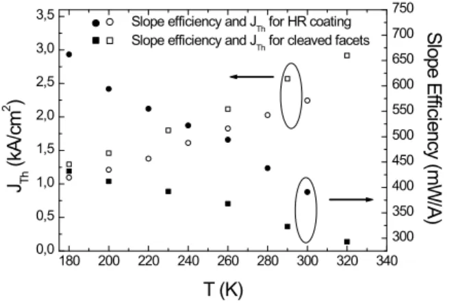
corresponding slope efficiency is 440 mW/A (530 mW/A). Figure 10 shows the evolution of the threshold current density and of the slope efficiency measured for two 2 mm long lasers, with HR coating (open and black circles) and with untreated cleaved facets (open and black squares). Similar experiments (not shown here) have also been performed on 1 mm lasers. The characteristic temperatures T0 are 160 K
and 180 K for the 2 and 1 mm long lasers. These values are in agreement with previous measurements on the standard processed lasers of section III. The threshold value for the HR coated device, in this range of temperature, is reduced of a factor 20%, while the T0 parameter remains unchanged. At
300 K, the slope efficiency is increased by a factor of 24% for a HR coated device. We have also deduced from these experiments the parameter T1describing the temperature
evo-7 180 200 220 240 260 280 300 320 340 0,0 0,5 1,0 1,5 2,0 2,5 3,0 3,5 J Th ( kA /c m 2 ) T (K)
Slope efficiency and JTh for HR coating
Slope efficiency and JTh for cleaved facets
300 350 400 450 500 550 600 650 700 750 S lo p e E ffic ie n cy (m W /A )
Fig. 10. Threshold current densityJT hand slope efficiency as a function of
temperature for a 2 mm long laser with rear facet HR coated (open and black dots), and for a 2 mm long laser with cleaved facets (open and black squares).
In both cases, theT0 parameter is 165 K.T1is 247 K for the cleaved facet
laser and 376 K for HR coated laser.
TABLE I
CHARACTERISTICS OF THE DIFFERENT LASERS
L1 L2 L3 L4 L5
Length (mm) 2 2 2 1 2
Mounting up up down down down
HR coating no no no yes yes
Gold layer no yes yes yes yes
Maximum Average power (mW) 49 78 102 100 174
Optimal Duty Cycle (%) 12 25 37 35 40
lution of the slope efficiency η defined as η(T ) = η0e−T /T1.
For 2 mm long lasers, T1is247 K for the cleaved facet laser
and376 K for the HR coated laser. The use of a HR coating
increases the value of this parameter by 50%.
In order to estimate the improvement obtained with the thick electroplated gold layer, we have tested the behavior of our lasers at room temperature and high duty cycles. We have measured the evolution of the average power for different duty cycles. The lasers were mounted on a thermoelectric cooler to maintain a constant background temperature. The pulse duration used for this experiment was 188 ns and the
repetition rate was varied from100 kHz to 3.2 MHz. Fig. 11
shows the average output power as a function of the duty cycle at a temperature of 293 K for a series of lasers of different
cavity configurations. This experiment shows the behavior of
5 different processings summarized in Table I.
First we compare lasers L1 and L2. These device have a 2mm cavity length, are mounted epi-layer up and have no HR coatings. However L1 does not have a thick gold heat spreading layer whereas L2 does have a gold layer. The maximum average power of L2 (78mW) is higher than that of L1 (48mW). Furthermore, the maximum average power of L2 occurs at a duty cycle of 25% twice as high as L1.
Next we compare lasers L2 and L3. The only difference between these devices is that L3 is mounted epi-layer down. In all other aspects the devices are nominally identical (with gold heat spreaders and cleaved facets). The maximum average power of L3 is 100mW at a duty cycle of 40%. Mounting
0 10 20 30 40 50 60 0 20 40 60 80 100 120 140 160 180 200 L1 L2 L3 L4 L5
A
ve
ra
g
e
P
o
w
e
r
(m
W
)
Duty Cycle (%)
Fig. 11. Maximum average optical power as a function of the duty cycle for
5 different lasers at T = 283 K. L1 (open dots) 2 mm long laser mounted
layer up with cleaved facets; L2 (open stars) 2 mm long laser mounted epi-layer up with electroplated gold epi-layer and cleaved facets; L3 (open triangles) 2 mm long laser mounted epi-layer down with electroplated gold layer and cleaved facets; L4 (black stars) 1 mm long laser mounted epi-layer down with electroplated gold layer and rear facet HR coated; L5 (black dots) 2 mm long laser mounted epi-layer down with electroplated gold layer and rear facet HR coated
devices epi-layer down is thus crucial and has a big effect on the thermal characteristics as it increases the optimal duty cycle up to 40%. Dissipation is more efficient in the case of epi-layer down mounted devices and the maximal optical intensity is also increased of 30%.
We now compare lasers L3 and L5. The difference between these devices is that L3 has cleaved facets and L5 has a facet HR coated. The effect of the HR mirror is an increase of the output power of 75% while no effect is observed on the optimal duty cycle. The maximum average power is 175mW at a duty cycle of 40%. Finally, L4 and L5 illustrate the effect of
the size of the laser cavity. These two lasers are mounted epi-layer down, have the rear facet HR coated and have a thick electroplated gold layer on the ridge. Both device present a maximum average power for a duty cycle of ∼40% with 175 mW for the 2 mm long device and100 mW for the 1 mm long
device. To our knowledge, these values are the best values reported so far for aλ = 9µm QCL.
This experiment shows in an unambiguous way, the effect of different fabrication processings on the lasing performance of the devices. Similar experiments have been performed with 3 different 3 mm long lasers, showing no improvement of the performance in terms of both emitted power and threshold val-ues, with respect to 2 mm long devices. The best performance is thus obtained for a 2 mm long laser, with the rear facet HR coated, with an electroplated gold layer and mounted epi-layer down.
With such a large ridge (24 µm), these lasers are not
optimized for room temperature CW operation. Nevertheless, the excellent performance obtained at high values of duty cycle are encouraging for room temperature applications. Fig. 12 shows the CW optical power as a function of the injected current for various temperatures for a laser with the same
0,0 0,5 1,0 1,5 2,0 2,5 0,0 0,1 0,2 0,3 0,4 270 K 260 K 240 K 220 K 200 K 77 K
P
o
w
e
r
(W
)
Current (A)
Fig. 12. Optical power as a function of current for a 2 mm long laser
with rear facet HR coated and a thick electroplated gold heat spreader in CW operation at various temperatures.
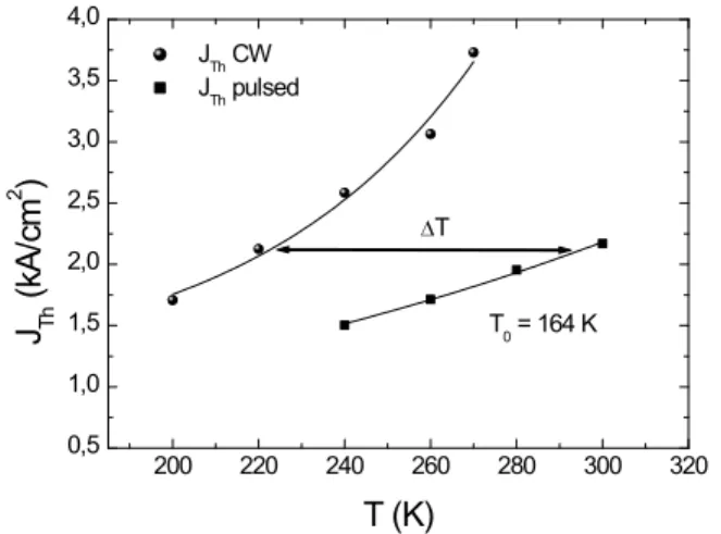
200 220 240 260 280 300 320 0,5 1,0 1,5 2,0 2,5 3,0 3,5 4,0 ∆T T0 = 164 K J Th ( kA /c m 2 ) T (K) JTh CW JTh pulsed
Fig. 13. Threshold current density as a function of temperature for a 2 mm
long laser, HR coated with electroplated gold layer, epi-layer down mounted, in pulsed (black squares) and CW (black dots) operation.
characteristics as L5 in Table I. At77 K, the optical power is 417 mW. CW operation is observed up to 278 K with 38 mW
of optical power at260 K.
V. THERMAL RESISTANCE OF THE LASERS WITH
ELECTROPLATED GOLD LAYER
As mentioned above, the limiting factor for CW operation is the ability of a device to evacuate the heat produced by the current injected in the active region. This ability depends on the thermal properties of the materials constituting the active region itself, the surrounding material and also on the design process.
We have determined, for every process design used in this paper, the thermal resistance by comparing the threshold current densities measured at different temperatures in pulsed and CW operation. The low values of duty cycle used in pulsed measurements ensure that no self-heating occurs in the active region. The large amount of heat dissipated in CW operation increases the active region temperature and thus the current threshold density. As shown in Fig. 13, we can deduce from these measurements an equivalent active region temperature increase ∆T=TAR-THS whereTAR is the
temperature of the active region in CW operation and THS is
the heat sink temperature. We can then determine, knowing the power dissipated at threshold in the device, a value of thermal resistance RT H defined as:
TAR= RT HUT hIT h+ THS (1)
where UT h and IT h are the DC voltage and intensity at
threshold.
Because of the anisotropy of thermal diffusion in semi-conductor superlattices, the width of a laser ridge has an effect on the measured thermal resistance which will not be studied in this work. We will normalize the measured thermal resistance by the area of the lasers. On our reference sample, a 2 mm long laser with a ridge width of 24 µm mounted up,
this measure yields a thermal resistance value of 30.0 K/W (1.44 × 10⁻²K.cm2/W ).
The same measurements performed on a laser similar to the reference laser, epi-layer up, and with a thick electroplated gold layer on the laser ridge brings a thermal resistance value of 14.5 K/W (6.96 × 10⁻³K.cm2
/W ), a factor 2 lower that
the one measured on the reference laser.
The thermal resistance measured on a 2 mm long laser with a thick electroplated gold layer on the laser ridge and mounted epi layer down is 9.0 K/W (4.32 × 10⁻³K.cm2/W ),
which represents a reduction of 40% with respect to a similar sample mounted up. The 3 mm long lasers with the same process design show a thermal resistance of 6.8 K/W (4.9 × 10⁻³K.cm2/W ). Finally, a 1 mm long laser with electroplated
gold layer mounted epi layer down shows a thermal resistance twice as high, RT h=17 K/W (4.08 × 10⁻³K.cm2/W ), which
scales correctly with a 2 or 3 mm long laser.
We will now compare our devices with the buried het-erostructure design. The 0.75 mm long and 12 µm wide
buried heterostructure laser described in Ref. [6] had a thermal resistance RT h = 19.4K/W = 1.75 × 10⁻³K.cm2/W . For
our epi-layer up mounted reference, the normalized thermal resistivity is 8 times higher while lasers with an electroplated gold layer have a much lower thermal resistivity but still about 2.3 times higher than the buried heterostructure one.
This precise determination of the thermal resistivity values confirms the trend already observed in Fig. 11 with the duty cycle values at which the maximum average power for these different process designs was measured. This section shows how low thermal resistivities (but still higher than those measured on the buried heterostructure of Ref. [6]) can be achieved with the addition of a heat spreader (thick electroplated gold layer) on top of the laser ridge.
VI. CONCLUSION
Different ways of producing high power InP based QCL by improving the heat dissipation have been studied: ion implantation and the use of an electroplated gold layer on top of the ridge. Proton implanted samples showed CW operation up to 293 K with 20 mW of output power. However, the insulating properties of the implanted layer breaks down at high temperature a gives rise to poor electrical characteristics. This technique, efficient in GaAs based structures, fails at
9
high temperatures in InP based devices. Lasers with a thick electroplated gold layer showed CW operation up to 278 K and 1 W of optical power at 280 K in pulsed operation. With such a process, the thermal characteristics of the lasers are improved with an output average power of 174 mW at a duty cycle of 40% measured at 10◦C for a 2 mm long laser.
REFERENCES
[1] J. Faist, C. Sirtori, InP and GaAs-based Quantum Cascade Lasers, in Long Wavelength Infrared Semiconductor Lasers, edited by H.K. Choi (J. Wiley and Sons, Hoboken, N.J., 2004.
[2] H. Page, S. Dhillon, M. Calligaro, C. Becker, V. Ortiz, C. Sirtori,
Improved CW Operation of GaAs-Based QC Lasers:Tmax = 150K,
IEEE Journal of Quant. Elec., 40, p 665-672, 2004.
[3] A. Evans, J.S. Yu, J. Davis, L. Doris, K. Mi, S. Slivken, M. Razeghi,
High-Temperature, High Power, Continous-Wave Operation of Buried Hetrostructure Quantum Cascade Lasers, Appl. Phys. Lett., 84, p
314-316, 2004.
[4] A.A. Kosterev, R.F. Curl, F.K. Tittel, C. Gmachl, F. Capasso, D.L. Sivco, J.N. Baillargeon, A.L. Hutchinson, A.L. Cho, Methane Concentration
and Isotopic Composition Measurements With a Mid-Infrared Quantum Cascade Laser, Optics Lett., 24, p1762-1764, 1999.
[5] D. Weidmann, F.K. Tittel, T. Aellen, M. Beck, D. Hofstetter, J. Faist, S. Blaser, Mid-Infrared Trace-Gas Sensing With a
Quasi-Continuous-Wave Peltier-Cooled Distributed Feedback Quantum Cascade Laser,
Applied Phys. B, 79, p 907-913, 2004.
[6] M. Beck, D. Hofstetter, T. Aellen, J. Faist, U. Oesterle, M. Ilegems, E. Gini, H. Melchior, Continuous Wave Operation of a Mid-Infrared
Semiconductor Laser at Room Temperature, Science, 295, p 301-305,
2002.
[7] H. Page, S. Dhillon, M. Calligaro, V. Ortiz, C. Sirtori, Optimized Device
Processing for CW Operation in GaAs Based QCL, Elect. Lett., 39, p
1053-1055, 2003.
[8] J.S. Yu, S. Slivken, A. Evans, L. Doris, M. Razeghi, High Power CW
Operation of a 6µm Quantum Cascade Laser at Room Temperature,
Appl. Phys. Lett., 83, p 2503-2505, 2003.
[9] J.S. Yu, A. Evans, J. Davids, L. Doris, S. Slivken, M. Razeghi,
Cav-ity Length Effects of High Temperature High Power Continuous Wave Characteristics in Quantum Cascade Lasers, Appl. Phys. Lett., 83, p
5136-5138, (2003).
[10] S. Slivken, Z. Huang, A. Evans, M. Razeghi, High Power (λ = 9µm)
Quantum Cascade Lasers, Appl. Phys. Lett., 80, p 4091-4093, 2002.
[11] D. Hofstetter, M. Beck,T. Aellen, J. Faist, U. Oesterle, M. Ilegems,
E. Gini, H. Melchior, Continuous Wave Operation of a 9.3µm Quantum
Cascade Laser on a Peltier Cooler, Appl. Phys. Lett., 78, p 1964-1966,
2001.
[12] J. Faist, M. Beck, T. Aellen, E. Gini, Quantum-Cascade Lasers based
on a bound-to-continuum transition, Appl. Phys. Lett., 78, p 147-149,
2001.
[13] J. Faist, F. Capasso, D.L. Sivco, C. Sirtori, A.L. Hutchinson, A.Y. Cho,
Quantum Cascade Laser, Science, 264, p 553-556, 1994.
[14] H. Page, P. Collot, A. de Rossi, V. Ortiz, C. Sirtori, High Reflectivity
Metallic Mirror Coatings for Mid-Infrared (λ ≈ 9µm) Unipolar
Semi-conductor Lasers, Semicond. Sci. Technol., 17, p 1312-1316, 2002.
[15] T. Ikegami, Reflectivity of Mode at Facet and Oscillation Mode in
Double-Heterostructure Injection Lasers, IEEE J. Quantum Electron., 8,
p 470-476, 1972.
[16] C. Sirtori, H. Page, C. Becker, V. Ortiz, IEEE J. Quantum Electron., 38, p 547-558, 2002.
[17] S.J Pearton, Mater. Sci. Rep., 4, p 313, 1990.
[18] J.P. Donnelly and C.E. Hurwitz, Proton Bombardment in InP, Solid State Electron., 20, p 727-730, 1977.
[19] J.S. Yu, S. Slivken, A. Evans, J. Davids, L. Doris, M. Razeghi, Very High
Average Power at Room Temperature From a 5.9µm Quantum Cascade
Lasers, Appl. Phys. Lett., 82, p 3397-3399, 2003.
Cl´ement Faugeras received the engineer degree from ’Institut Nationnal des Sciences Appliqu´ees’ de Lyon, France, and the Ph.D. degree in physics from the University Joseph Fourier, Grenoble, France, in 2003. His studies focused on the infrared response of low dimensional electronic systems in high magnetic fields. In 2004, he joined the group of Quantum Phenomena and Devices at University Paris VII where he is currently working on high power InP based quantum cascade lasers.
S´ebastien Forget was born in Nancy, France, in 1976. He received the Engineer degree from the Ecole Nationale Sup´erieure de Physique de Mar-seille, France, in 1998 and the PhD degree in Physics from the University of Paris XI (France) in 2003. His studies focused on diode-pumped solid-state laser and amplification systems, and more specifi-cally on pulsed UV lasers and their application to time-resolved fluorescence microscopy. In 2004, he joined in a post-doctoral position the Mat´eriaux et Ph´enom`enes Quantiques team at the University of Paris VII, where he worked on high power InP-based Quantum Cascade Lasers and second harmonic generation in GaAs-based QCL. He is now Maˆitre de Conf´erences at the University of Paris XIII, France, where his research activity focuses on VUV lasers and Organic Light-Emitting Diodes. Dr. Forget is the author or co-author of about 30 journal and conference papers and holds a patent on novel laser amplification scheme.
Elizabeth Boer-Duchemin received the Ph.D. de-gree in applied physics from the California In-stitute of Technology in Pasadena, CA, in 2001. Her dissertation research involved the optical and electrical properties of silicon nanocrystals. From 2001-2003 she was a research engineer at Alcatel Opto+, Marcoussis, France, working on high power semiconductor pump lasers for optical amplifiers, before spending a year at Thales Research and Tech-nology, (in collaboration with Ecole Polytechnique and the Institut d’Optique) in Orsay, France. Her current research focuses on the manipulation of molecules and nanoparticles using scanning field microscopies as a junior professor at the University of Paris 11, Orsay, France.
Hideaki Page was born in Kyoto, Japan, in 1971 and raised in the U.K. He received the Ph.D de-gree from the university os Surrey, Surry, U.K., in 1998, studying bandgap dependent loss mechanisms in GaAs-based diode lasers with externally applied hydrostatic pressure. For the last five years, he has been with Thales Research and Technology, Orsay, France. His current research interests focus on all as-pects of the design and characterization of quantum cascade lasers and their applications.
Jean-Yves Bengloan was born in France in 1977. He received the M.S. degree in physics in 2001 from Orsay University, France. He is currently working towards a Ph.D. degree at Thales Research and Technology, France. His research focuses on the de-sign and characterisation of GaAs Quantum Cascade structures.
Olivier Parillaud was born in 1964 in Palaiseau, France. He obtained his Ph. D. Degree in Physics in 1996 from the University Blaise Pascal of Clermont-Ferrand (France). After post-doctoral stays in the France Telecom Research Center (CNET) in Bagneux and in the CRHEA - CNRS (Centre de Recherche sur l’H´et´ero´epitaxie et ses Applications) in Valbonne, he joined the Institute of Micro- and Optoelectronics of the Swiss Federal Institute of Technology of Lausanne (Switzerland), where he worked on Gallium Nitride growth and applications. He is in Thales Research and Technology - France since February 2000 and is responsible for the realization of optoelectronic epitaxial structures by MOVPE such as high power and high brightness laser diodes at 808nm
and 980nm on GaAs, edge emitting PF and DFB lasers from 1.3µm to 1.7 µm
on InP, photodiodes, etc He is author and co-author of 30 papers published in referred journal and conference proceedings.
Michel Calligaro was born in Bordeaux, France, on May 11, 1948. He graduated from the ”Institut Nationnal des Sciences Appliqu´ees”, Toulouse, France, in 1971, and received the 3rd Cycle Doctor’s degree in 1975. He joined Thales Research and Technology, Orsay, France, in 1973, where he has been working on microwaves diodes and semiconductors lasers. He has been involved in the design and technology of silicon PIN diodes, GaAs IMPATT diodes, Si IMPATT diodes, and InP GUNN diodes for applications between 10 and 94 GHz. Since 1995, he has been involved in the technology of various semiconductor lasers and light-emitting diodes and he has been involved in several European projects: RAINBOW, GHIZO, OFCORSE 2 and ULTRABRIGHT.
Carlo Sirtori received the PhD in physics, from the University of Milan, Italy, in 1990. The same year joined Bell Laboratories, where he was one of the prime member of the team that in 1994 invented the Quantum Cascade (QC) laser. In 1997, he joined THALES R&T and in 2000 became the head of the ”Semiconductor Laser Group”, leading the research and development of semiconductor lasers from the visible to the mid-infrared. Since 2002 he is full professor at the University Denis Diderot in Paris, while carrying on his research activities still with THALES R&T. His main research interests are today on quantum phenomena in nanostructures and QC lasers. He has co-authored over 110 papers, has given more than 50 invited talks at international conferences and hold 20 patents.
Marcella Giovannini was born in the United States in 1970. She received her Ph.D degree in physics from the Swiss Federal Institute of Technology in Lausanne, Switzerland. Her studies focused on low-dimensional properties of metallic structures. After a first postdoctoral position on photoemission studies of mono-atomic metallic chains, she joined the group of J´erˆome Faist in Neuchˆatel, Switzerland, where she participated in the development of InP-based and GaAs-InP-based QC lasers.
J´erˆome Faist was born in Switzerland on January 23, 1962. He received the Ph.D. degree in physics from the Swiss Institute of Technology, Lausanne, in 1989. His study focused on vertical-cavity surface emitting lasers and optical modulators.
After a two-year post-doctoral position in IBM, he joined Bell Laboratories, Lucent Technologies, Murray Hill, NJ, in September 1991, where his worked focused on the physics of intersubband transitions and the development of the quantum cascade laser. In 1997, he became Full Professor at the university of Neuchatel, Neuchatel, Switzerland, where his work currently focuses on the development of mid- and far-infrared intersubband lasers.
Dr Faist is a member of the American Association for the Advancement of Science.