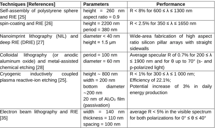
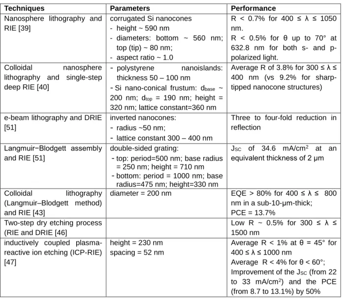
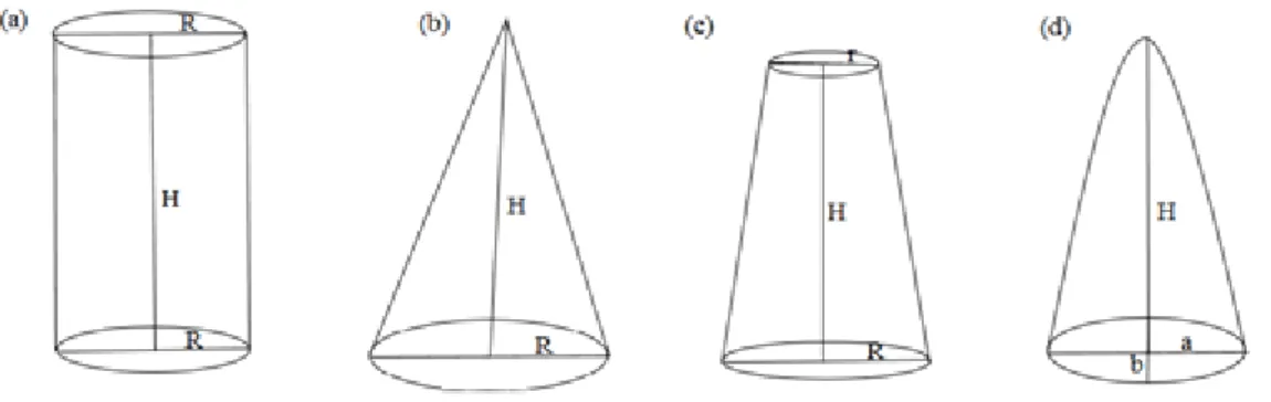
Design and optimization of silicon nanostructures
Texte intégral
Figure


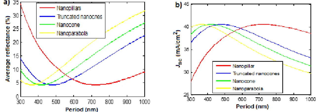

![Table 4: Summary of the performance of the antireflective structures AR structures Rw [%] Jsc [mA/cm²] Pillars 3.0792 41.1799 Cones 2.7507 41.3114 Truncated cones 2.0067 41.6274 Parabolas 1.2222 41.9607](https://thumb-eu.123doks.com/thumbv2/123doknet/12949646.375789/11.892.285.584.141.338/summary-performance-antireflective-structures-structures-pillars-truncated-parabolas.webp)
Documents relatifs
- Single and multicrystalline silicon wafers for terrestrial solar cell application can be prepared either by semi- and unconventional bulk growth methods including post
Warta, “Modeling majority carrier mobility in compensated crystalline silicon for solar cells,” Solar Energy Materials and Solar Cells, no3. Que, “Influence of the compensation
Un autre prolongement intéressant et s’inscrivant dans un cadre plus scolaire, serait de mesurer les effets de ce programme de développement de l’empathie
Then a new concept of the drift type photovoltaic effect in terms of the field dependent photo- carrier generation process and carrier collection efficiency is introduced, As the
Although no clear evidence of coherent reduction of the thermal conductivity could be shown in the fishbone PnCs, the effect of surface scattering is, in that
The surface passivation properties provided by the poly-Si(B)/SiO x structure fabricated on KOH-polished c-Si wafers were further improved by depositing a
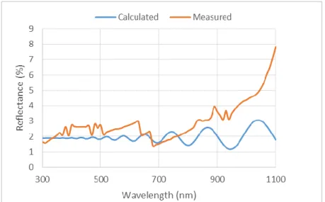
Supporting Information provides refractive indices (n and k) used for FDTD calculations, additional data from measurements and numerical calculations, detailed numerical analysis of
Dans cette section nous allons étudier l’effet de variation de la distance entre les éléments rayonnants sur le diagramme de rayonnement d’un réseau de 6 antennes uniformes,
