HAL Id: in2p3-01265779
http://hal.in2p3.fr/in2p3-01265779
Submitted on 13 Jan 2020HAL is a multi-disciplinary open access archive for the deposit and dissemination of sci-entific research documents, whether they are pub-lished or not. The documents may come from teaching and research institutions in France or abroad, or from public or private research centers.
L’archive ouverte pluridisciplinaire HAL, est destinée au dépôt et à la diffusion de documents scientifiques de niveau recherche, publiés ou non, émanant des établissements d’enseignement et de recherche français ou étrangers, des laboratoires publics ou privés.
Front-end electronics for the FAZIA experiment
F. Salomon, P. Edelbruck, G. Brulin, B. Borderie, A. Richard, M.F. Rivet, G.
Verde, E. Wanlin, A. Boiano, G. Tortone, et al.
To cite this version:
F. Salomon, P. Edelbruck, G. Brulin, B. Borderie, A. Richard, et al.. Front-end electronics for the FAZIA experiment. Topical Workshop on Electronics for Particle Physics (TWEPP2015), Sep 2015, Lisbon, Portugal. pp.C01064, �10.1088/1748-0221/11/01/C01064�. �in2p3-01265779�
Journal of Instrumentation
Front-end electronics for the FAZIA experiment
To cite this article: F. Salomon et al 2016 JINST 11 C01064
View the article online for updates and enhancements.
Related content
Validation of a paediatric thyroid phantom using different multidetector computed tomography models
M Alsabbagh, L Y Ng, A A Tajuddin et al.
-A new approach to front-end electronics interfacing in the ATLAS experiment
J. Anderson, A. Borga, H. Boterenbrood et al.
-FELIX: a PCIe based high-throughput approach for interfacing front-end and trigger electronics in the ATLAS Upgrade framework
J. Anderson, K. Bauer, A. Borga et al.
-Recent citations
Energy response and identification efficiency of CsI(Tl) crystals irradiated with energetic protons
C. Frosin et al
-The FAZIA setup: A review on the electronics and the mechanical mounting
S. Valdré et al
-OSCAR: A new modular device for the identification and correlation of low energy particles
D. Dell’Aquila et al
2016 JINST 11 C01064
Published by IOP Publishing for Sissa Medialab
Received: October 30, 2015 Revised: December 8, 2015 Accepted: December 14, 2015 Published: January 26, 2016
Topical Workshop on Electronics for Particle Physics 2015, September 28th– October 2nd, 2015
Lisbon, Portugal
Front-end electronics for the FAZIA experiment
The FAZIA collaboration
F. Salomon,1,∗P. Edelbruck,1G. Brulin,1B. Borderie,1A. Richard,1M.F. Rivet,1,†G. Verde,1,6 E. Wanlin,1A. Boiano,2G. Tortone,2G. Poggi,3M. Bini,3G. Casini,3S. Barlini,3G. Pasquali,3 S. Valdré,3M. Petcu,4R. Bougault,5N. Le Neindre,5R. Alba,14E. Bonnet,7M. Bruno,8 A. Chbihi,7M. Cinausero,10D. Dell’Aquila,2H. De Préaumont,5J.A. Duenas,13Q. Fable,2 D. Fabris,10L. Francalanza,2J.D. Frankland,7E. Galichet,1,9F. Gramegna,10D. Gruyer,3 M. Guerzoni,9A. Kordyasz,12T. Kozik,11R. La Torre,2I. Lombardo,2O. Lopez,5J. Mabiala,10 C. Maiolino,14T. Marchi,10P. Maurenzig,3A. Meoli,2Y. Merrer,5L. Morelli,8A. Nannini,6 A. Olmi,3A. Ordine,2M. Pârlog,4,5G. Pastore,6S. Piantelli,3E. Rosato,2,†D. Santonocito,14 E. Scarlini,3G. Spadacini,2A. Stefaninni,3E. Vient5and M. Vigilante2
1Institut de Physique Nucléaire, CNRS/IN2P3, Univ. Paris-Sud, Université Paris-Saclay, 91406 Orsay Cedex, France
2INFN – Sezione di Napoli, Complesso Universitario di Monte S. Angelo, 80126 Napoli, Italy 3Dipartimento di Fisica, Università di Firenze and INFN Sezione di Firenze,
50019 Sesto Fiorentino (FI), Italy,
4National Institute for Physics and Nuclear Engineering, Bucharest-Mãgurele, Romania 5LPC, CNRS/IN2P3, ENSICAEN et Université de Caen, F-14050 Caen-Cedex, France 6INFN – Sezione di Catania, 95123 Catania, Italy
7GANIL, CEA et CNRS/IN2P3, B.P. 5027, 14076 Caen-Cedex 05, France
8Dipartimento di Fisica e Astronomia, Università di Bologna and INFN, Sezione di Bologna, 40126 Bologna, Italy
9Conservatoire National des Arts et Métiers, 75141 Paris cedex 03, France 10INFN LNL Legnaro, viale dell’Università 2, 35020 Legnaro (Padova) Italy
11Jagiellonian University, Institute of Nuclear Physics IFJ-PAN, 31342 Kraków, Poland 12Silesian University, University of Silesia, Katowice, Poland
13Departemento de Fisica Aplicada, FCCEE Universidad de Huelva, 21071 Huelva, Spain 14INFN – Laboratori Nazionali del Sud, 95123 Catania, Italy
E-mail: [email protected]
∗Corresponding author. †Deceased.
2016 JINST 11 C01064
Abstract: FAZIA is a multidetector specifically designed to optimize A and Z reaction productidentification in heavy-ion collision experiments. This multidetector is modular and based on three-layer telescopes made of two silicon detectors followed by a thick (10 cm) CsI(Tl) scintillator read-out by a photodiode. Its electronics is fully digital. The goal to push at maximum identification capability while preserving excellent energy resolution, can be achieved by using pulse-shape analysis techniques and by making an intensive use of high-speed flash ADCs. This paper presents the front-end part of the electronics.
Keywords: Front-end electronics for detector readout; Digital electronic circuits; Analogue elec-tronic circuits; Data acquisition circuits
2016 JINST 11 C01064
Contents 1 Introduction 1 2 System architecture 1 2.1 General 1 2.2 Regional level 2 2.3 Block level 23 The front-end card 3
3.1 Synopsis of the card 3
3.2 High voltage devices 4
3.3 Pulse generator for analog chains 4
3.4 PIC micro-controller 4
3.5 Preamplifiers 5
3.6 Analog chains and data processing 5
3.7 Digital processing 6
3.8 Overview 6
4 Experimental results 7
5 Conclusion 7
1 Introduction
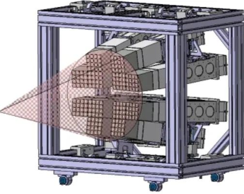
The multidetector FAZIA is aimed at detecting and identifying particles and fragments produced in heavy-ion reactions at low and intermediate energies. The final detection array will cover a sizeable portion of the solid angle with three-layer telescopes (Si + Si + CsI(Tl)). The goal consists in obtaining unit identification for charges up to Z = 70 and masses up to A = 50 [1]. This goal will be achieved using dedicated developed detectors and using electronics with novel pulse-shape analysis techniques [2] based on high speed analog-to-digital converters with rates up to 250 Ms/s and 14 bits resolution. The whole electronics will be embedded in the proximity of the telescopes inside the vacuum chamber. Figure1shows a configuration of the FAZIA demonstrator for which the front end electronics is dedicated.
2 System architecture 2.1 General
The multidetector is organised into three hierarchical levels: i) the regional level consisting of the DAQ system controlling the whole detector, ii) the block level consisting of the block which is a system embedding the front-end electronics and 16 telescopes, iii) the front-end level which is the Front-end electronic card managing two telescopes.
2016 JINST 11 C01064
Figure 1. A configuration of the FAZIA demonstrator composed of 12 blocks.
2.2 Regional level
At the top of the tree and located outside of the vacuum chamber, the “regional level” is tightly connected to the DAQ. It has a complete view of the whole multidetector in real time and has two important roles: 1) gather requests from telescopes, make and dispatch global trigger decisions; 2) collect acquisition data, build events and upload the data to the DAQ system.
2.3 Block level
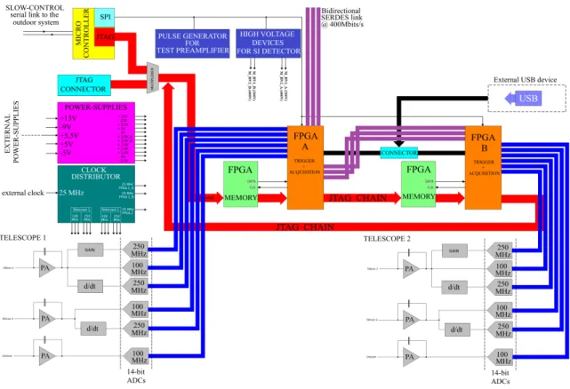
The second level of the system corresponds to the basic building block of FAZIA from a geometrical point of view. The block is presented on figure2. It consists of a total of 16 telescopes. The blocks located in the vacuum chamber communicate with the regional level through a high speed optical fiber. Each block is supported by a copper plate which also allows for cooling. Each block features three internal cards for the I/O operations and for the control of the eight FEE cards. These three latter cards and the block mechanics have been built by the italian side of the FAZIA collaboration [3]. The EMC (electromagnetic compatibility) guidelines have been applied by IPN Orsay to review and modify the shield structure.
Figure 2. One block.
2016 JINST 11 C01064
One block includes:• The back side: a block card for digital control and two cards for power-supply. As these power-supply cards are very noisy, they are sealed under a metallic enclosure. These three cards have been designed by INFN in Naples.
• The middle of the block: 8 front-end cards, each one managing two triple telescopes. These cards are going to be described further in this paper and have been designed by IPN Orsay. • The front side which is a set of 16 telescopes. Each telescope is composed of three layers:
300–500 µm Si (Si1 and Si2 with an active area of 20×20 mm2) — 10 cm CsI(Tl) scintillator
read-out by a photodiode. Each detector is directly connected to the input connectors of the front-end card presented below. As the card manages two telescopes, six input connectors are embedded on this card.
3 The front-end card 3.1 Synopsis of the card
Figure 3. Synopsis of the FEE card.
Each front-end card manages two telescopes with a total of 6 channels: 4 silicon detectors and 2 photodiodes. When staring at this synopsys (figure3), we observe two VIRTEX-5 XILINX FPGA chips and their respective memories. We also observe two similar groups of three charge
2016 JINST 11 C01064
preamplifiers, analog chains and analog-to-digital converters (ADC). As the card manages twotelescopes, each FPGA, each group of three preamplifiers, each group of analog chains and each group of analog-to-digital converters are dedicated to one telescope.
Another feature concerns a unique clock distributor block whose purpose is to generate 100 MHz and 250 MHz frequencies from an external clock at 25 MHz. The 100 MHz frequency is useful to clock high speed ADC for charge signal waveforms and both FPGA devices. The 250 MHz frequency is used to clock high speed ADC for current signal waveforms and the ADC for 250 MeV charge waveforms.
The low-voltage power-supply block includes 4 switching regulators and more than 20 linear regulators.
Other features are available on these cards. Four high voltage devices for silicon detector biasing, one pulse generator and a multi-function controller are also embedded. These features will be deeply described further in this section.
3.2 High voltage devices
Four high voltage devices are embedded on the board; high voltages are generated from a common 48 V input. Their architecture is based on a switching regulator and a transformer. Their purpose is to bias the silicon detectors of the two telescopes. The HV device for Si1 of the telescope can ramp up to 300 V with a precision of 0.1 V. The HV device for Si2 can ramp up to 500 V with the same precision. The HV functions and values are remotely controlled. Inside each HV device, an additional circuitry built on a micro-controller and a 16-bit ADC has been added in order to measure the reverse current of a silicon detector flowing through a 10 MΩ charge resistor. When this reverse current increases, the HV device automatically increases its voltage output to compensate the potential difference and to maintain the biasing voltage of the silicon detector at constant value. The precision of the current measurement is about 30 nA. For the next generation of cards, this precision will be increased thanks to a more robust dielectric to integrate inside the PCB. Moreover, this additional circuitry can indirectly measure the output voltage for each HV device.
The developed HV device represents a new and original solution, within the nuclear physics community, as it is integrated into one single electronic card operating under vacuum.
3.3 Pulse generator for analog chains
A pulse generator has been built on the front-end card in order to obtain the preamplifier response. This response allows testing the preamplifiers themselves and their analog channels; it is also useful to verify possible amplification changes during data taking in experiments. Furthermore, this response allows controlling the linearity of the amplification chain and calculating the conversion between MeV and volt. Different settings are available. The operator can change the amplitude, the frequency, and the duty cycle of the pulse generator.
3.4 PIC micro-controller
8-bit micro-controller on the card executes a number of functions. It is capable to receive and execute commands coming from outside through a serial slow-control link. For the high voltage devices, it sets the output high voltage value and reads, by means of a specific ADC, current
2016 JINST 11 C01064
measurements flowing through the detector. It is capable to take automatically some decisions inorder to regulate the output voltage, depending on the current value. This controller regulates the characteristics of the pulse generator signal such as the amplitude, the frequency and the duty cycle. It can write and read by SPI link the FPGA registers designed in VHDL. The PIC micro-controller also gets temperature values coming from embedded sensors located in several critical positions on the cards. Finally, it can also drive the JTAG chain to remotely program the FPGA memory. However this function has not been implemented yet.
3.5 Preamplifiers
On the card, six charge preamplifiers are embedded. Their architecture is based on a folded cascode amplifier. A circuitry added at their output stage is aimed at tuning the output offset voltage. This function allows one to set the analog chain base line at the bottom level of the ADC input range. 3.6 Analog chains and data processing
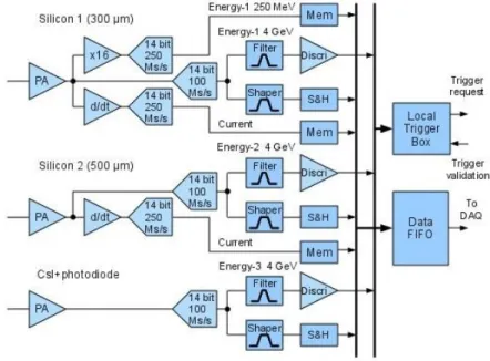
Each telescope includes a total of 3 preamplifiers (one per detector) connected to a total of 6 data channels as shown on figure4. The preamplifier output dynamic range is 8 V for a total energy of 4 GeV, providing a sensitivity of 2 mV/MeV for both Si1 and Si2.
Figure 4. Data processing for the telescope.
Three channels come from Si1. In the first channel, the output of Si1 is amplified by 16 and this signal is processed by a 250 Mbit/s ADC 14 bit for the high gain/speed line. This channel properly manages the lightest products of nuclear reactions depositing a rather small amount of energy. Moreover, thanks to the fast and precise ADC, it allows for good timing and energy measurements. The second channel corresponds to the high energy range of Si1. This energy range is 4 GeV full scale at 100 Mbit/s 14 bits, which is sufficient to accommodate the energy released by the heaviest and more energetic fragments of reactions. This channel also issues the trigger request signal.
2016 JINST 11 C01064
The third channel processes the current generated by Si1 when hit by a charged particle. Thecurrent signal is obtained from an analog charge preamplifier output derivation based on a differential operational amplifier and it is sampled at 250 Ms/s and 14 bits. This channel offers the most important feature of the FAZIA detector. Indeed, the current signal represents an accurate image of the charge collection process within the detector and allows for obtaining the best identification performances via pulse-shape analysis for ions stopping in the first stage of the telescope [4,5].
The Si2 output is split in two channels. The first one is the high-range energy line, equal to the corresponding one for Si1. The second is the current channel designed similarly to the Si1 case.
The last channel processes the scintillation pulses produced in the CsI(Tl) and read by a photodiode. The energy range is 500 MeV full scale (Si-equivalent) at 100 Mbit/s 14 bits. A special online data processing for particle identification is performed, based on the analysis of the slow / fast components of the light emission of the CsI(Tl) crystal.
3.7 Digital processing
Each front-end card embeds two FPGA devices, one for each telescope. Each FPGA can read out the six high speed analog-to-digital converters. It can compute the high resolution energy through digital filtering. It can also generate local triggers, data packing and transmission to the acquisition system at a speed of 400 Mbits/s.
3.8 Overview
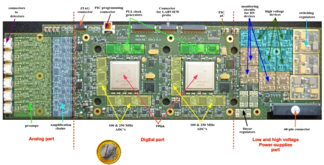
Figure 5. Picture of the FEE card. The 1AC coin is meant to give the scale.
The picture of a card is displayed on figure5. The area of this card (299×88 mm2) is subdivided
into three parts. The first one starting from the left side embeds all the low-noise analog electronics. At the opposite side (right part), the FEE hosts the switching power-supplies which are noisy and thus are designed far from the analog stages. In the middle part, FPGA components, converters
2016 JINST 11 C01064
and frequency synthesizers are mounted. The printed circuit board is a 16-layer one on which 1700components are only located on the top surface.
The power consumption of a card is about 29 W. The heat dissipation of this power is done by a copper plate pressed on the FPGA upper side. This copper plate is linked to the main shelf of the card. The main shelf is finally mounted on the main cooled copper plate of the block (see2.3). This copper plate made by INFN in Naples has internal pipes for cooled liquid flow.
4 Experimental results
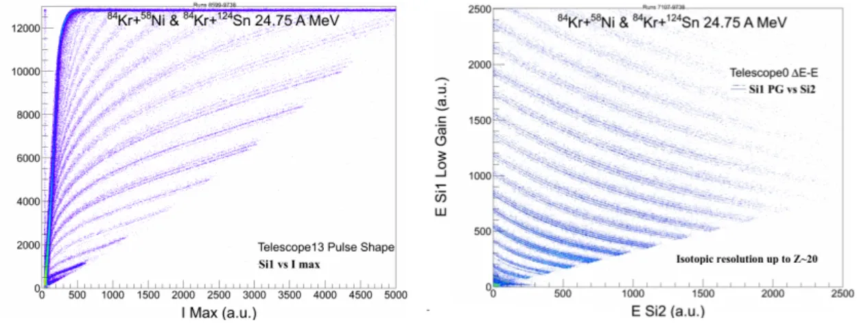
In December 2014, a test experiment was carried out at the LNS of Catania (Italy), using a complete FAZIA block. Thus 8 front-end cards have been fully tested in beam. We obtained small noise measurements for the different channels. For instance, the noise of the first silicon low range channel was about 1.8 mV. As a matter of fact, the overall behaviour was satisfactory and we could identify the different detected isotopes (see figure6).
Figure 6. A and Z identification; left — in the first Si detector with ESi1 vs. maximum current (Imax); right — standard ∆E/E plot from the two Si detectors.
5 Conclusion
The commissioning run of FAZIA has demonstrated the capability to integrate inside a vacuum chamber all the electronics required for silicon detectors and scintillators read-out by photodiodes. This very innovative and challenging electronics includes preamplifiers, analog chains, high speed converters, read-out logic, generated and regulated high voltage devices and pulse generator for analog chains. Good results have been obtained. The next FAZIA programme foresees the production of 64 updated FEE cards in order to build the complete 12-block demonstrator in 2016. Moreover, the commissioning run has proved the feasibility of some electronic features such as the HV device architecture. It has also proved that it is possible to integrate, on the same multi-layer card, some noisy power-supplies (such as switching regulators) with sensitive low-noise preamplifiers whose power-supply rejection ratio is not high. This integration has been made by applying strict EMC and PCB design guidelines.
2016 JINST 11 C01064
References[1] R. Bougault et al., The FAZIA project in Europe: R&D phase,Eur. Phys. J. A 50(2014) 47and
references therein.
[2] H. Hamrita et al., Charge and current-sensitive preamplifiers for pulse shape discrimination techniques
with silicon detectors,Nucl. Instrum. Meth. A 531(2004) 607[nucl-ex/0407009].
[3] Web site Fazia collaboration,http://fazia.in2p3.fr.
[4] S. Carboni et al., Particle identification using the ∆E-E technique and pulse-shape discrimination with
the silicon detectors of the FAZIA project,Nucl. Instrum. Meth. A 664(2012) 251.
[5] N. Le Neindre et al., Comparison of charged particle identification using pulse-shape discrimination
and ∆E-E methods between front and rear side injection in silicon detectors,Nucl. Instrum. Meth. A 701(2013) 145.