HAL Id: hal-02958095
https://hal.archives-ouvertes.fr/hal-02958095
Submitted on 7 Oct 2020HAL is a multi-disciplinary open access archive for the deposit and dissemination of sci-entific research documents, whether they are pub-lished or not. The documents may come from teaching and research institutions in France or
L’archive ouverte pluridisciplinaire HAL, est destinée au dépôt et à la diffusion de documents scientifiques de niveau recherche, publiés ou non, émanant des établissements d’enseignement et de recherche français ou étrangers, des laboratoires
Blue phosphorene reactivity on the Au(111) surface
Wei Zhang, Hanna Enriquez, Xuan Zhang, Andrew Mayne, Azzedine
Bendounan, Yannick Dappe, Abdelkader Kara, Gérald Dujardin, Hamid
Oughaddou
To cite this version:
Wei Zhang, Hanna Enriquez, Xuan Zhang, Andrew Mayne, Azzedine Bendounan, et al.. Blue phospho-rene reactivity on the Au(111) surface. Nanotechnology, Institute of Physics, 2020, 31 (49), pp.495602 - 495609. �10.1088/1361-6528/abb26c�. �hal-02958095�
Blue Phosphorene Reactivity on the Au(111) Surface
Wei Zhang1, Hanna Enriquez1, Xuan Zhang2, Andrew J. Mayne1, Azzedine Bendounan3,
Yannick J. Dappe4, Abdelkader Kara5, Gérald Dujardin1, and Hamid Oughaddou1,6*
1Université Paris-Saclay, CNRS, Institut des Sciences Moléculaires d’Orsay, 91405 Orsay,
France
2
School of Materials Science and Physics, China University of Mining and Technology, Xuzhou, 221116, PR China.
3
TEMPO Beamline, Synchrotron SOLEIL, L’Orme des Merisiers Saint-Aubin, B.P.48, 91192 Gif-sur-Yvette, France
4
Université Paris-Saclay, CNRS, CEA, Service de Physique de l'Etat Condensé 91191 Gif-sur-Yvette, France
5
Department of Physics, University of Central Florida, Orlando, FL 32816, USA
6
Département de physique, Université de Cergy-Pontoise, 95031 Cergy-Pontoise, France
Abstract: The synthesis of blue phosphorene by molecular beam epitaxy (MBE) has recently come under the spotlight due to its potential applications in electronic and optoelectronic devices. However, this synthesis remains a significant challenge. The surface reactivity between the P atoms and the Au atoms should be considered for the P/Au(111) system. In the MBE process, the temperature of the substrate is a key parameter for the growth of blue phosphorene. During the initial growth stage, irregularly shaped Phosphorus clusters grow on top of Au(111) surface at room temperature. When the substrate temperature is increased, these clusters transform into a phosphorene-like structure with a honeycomb lattice. An atom exchange reaction is observed between the P and first layer Au atoms under thermal activation at higher temperature, where the P atoms replace Au atoms to form a blue phosphorene structure within the top Au layer and at the step edges.
Keywords: phosphorene, two-dimensional materials, low temperature scanning tunneling microscopy, DFT calculation
1. Introduction
Black phosphorus, like graphite, is one of the few layered crystals in which single atomic layers stack together through van der Waals interactions instead of covalent bonds [1, 2]. As a semiconductor, black phosphorus has a natural direct band gap of ~0.3 eV [3-5]; this can be tuned by choosing the number of layers or by applying in-plane strain [6-9]. Black phosphorene, composed of a monolayer of black phosphorus, is predicted to have direct band gap of ~1.5 eV [10, 11], while retaining the characteristics that are to distinct to 2D materials, specifically a high carrier mobility. These properties makes it an ideal candidate for future electronic and optoelectronic devices with high on/off ratios [5, 12, 13].
Blue phosphorus is a stable allotrope of the layered phosphorus structure. A single layer of blue phosphorene is a semiconductor with an indirect band gap of approximately 2 eV [14]. However, bulk blue phosphorus does not exist in nature so that the controlled synthesis of blue phosphorene, based on the MBE method, is a necessary step for large-scale applications. So far, few studies have been reported on the epitaxial growth of phosphorene under ultrahigh-vacuum conditions [15-18]. In our recent study of the growth of blue phosphorene on Au(111) surface, we found that the phosphorene sheet formed a (5 × 5) structure with a measured band gap of at least 0.8 eV [17]. It is worth noting that in the process of preparing bulk black phosphorus from red phosphorus, the addition of small quantities of Au, Sn and SnI4 to the black phosphorus has led to the observation of additional structural phases, for
example, the compound Au3SnP7. This indicates that chemical reactions between gold and
phosphorus are possible [19, 20]. In recent experiments on few-layered black phosphorus and single-layer blue phosphorene, significant chemical reactivity was observed [21,22]. Therefore, the reactivity of phosphorus on the Au(111) surface should be considered during growth. Although the growth behavior of P clusters on Au(111) substrate has been reported in
the literature, the surface reactivity was not considered in the ab initio calculations used to model the P/Au(111) system [23]. Furthermore, the growth process and growth mechanism of phosphorene superstructure on Au(111) remains to be fully understood.
In this article, we shed light on the first steps of phosphorus growth on Au(111), using in situ low temperature scanning tunneling microscopy (LT-STM), Auger electron spectroscopy (AES) and low-energy electron diffraction (LEED) combining with density functional theory (DFT) calculations.
We observe that P atoms form irregularly shaped P-clusters on Au(111) at room temperature (RT), which then re-organize into phosphorene-like structure with a (5 × 5) superstructure at higher temperature. We demonstrate that the P atoms do not merely adsorb on the surface but exchange their positions with Au atoms at high temperature. The ejected Au atoms form dendritic structures at the terrace edges. There are several examples of the substitution of a surface metal atom by an adsorbing Group 14 atom; some form stable alloys [24-27], others disappear as more atoms are adsorbed [28, 29]. While alloy formation of the heavier Group 15 atoms Sb and Bi on Ag(111) and Cu(111) has been studied [30-32], this is a new observation of substitution behavior with phosphorus atoms.
2. Experimental Section
2.1 Materials and Characterization
We used a commercial Au(111) polished single crystal. The crystal substrate was cleaned by several cycles of Ar+ ion sputtering (650 eV at 6 × 10⁻⁶ mbar) and subsequent annealing at 770 K. Phosphorus atoms were deposited on the Au(111) substrate by evaporation from a Knudsen source loaded with black phosphorus. The Au(111) surface was kept at room temperature during the deposition. The sample was then analyzed as grown and after a
post-annealing at 530 K for 30 min. The experiments were performed using the standard tools for surface characterization: a Low-energy electron diffraction (LEED) for surface structure, an Auger electron spectrometer (AES) for chemical analysis of elements, and a low temperature Omicron scanning tunneling microscope (LT-STM at 77 K) for atomic scale surface characterization. The pressure in the preparation chamber is in the low 10-10 mbar range. The tip was made from tungsten wire (0.25 mm in diameter) by electrochemical etching. STS experiments were acquired using a lock-in amplifier with a modulation voltage of 10 mV and a frequency of 5127.7 Hz.
2.2 Computational Method
All first-principle DFT calculations were performed with VASP using version 5.4.1 [33-35], which implements the projector augmented wave (PAW) method [36, 37]. The present calculations were run using the GGA-PBE functional [38]. To model the Au(111) surface, a 4-layer slab was constructed, with each layer containing 12 atoms, to from a 3 × 4 lattice. The bulk Au lattice constant at 0 K was 4.17 Å [39]. To mimic the high temperature structures, the lattice constant was multiplied by 1.005 and 1.01. Using the 0 K lattice constant of a0 = 4.17
Å, and a linear coefficient of thermal expansion of 14 × 10-6/K, 1.005 × a0 corresponds to a
lattice constant at T = 357 K and 1.01 × a0 corresponds to a lattice constant at T = 714 K.
In the direction perpendicular to the surface, each slab is separated from the neighboring ones by a vacuum of about 22 Å between slabs. Structural relaxation was performed using the conjugate gradient (CG) method [40, 41], with the force criterion set to 0.02 eV/Å. The plane wave cutoff was set to 400 eV, and the Brillouin zone was sampled using a 6 × 4 × 1 Monkhorst-Pack grid.
3. Results and Discussion
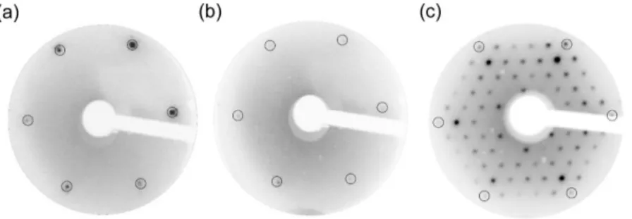
In figure 1, the LEED patterns are presented. Figure 1(a) shows the six principle spots corresponding to the (1 × 1) unit cell of the clean Au(111) substrate. These spots are surrounded by satellite spots from the well-known (22 × √3) reconstruction of Au [42]. These satellite spots are not as sharp as the more intense Au(1 × 1) spots. After deposition of 0.5 ML of P on the Au(111) surface at RT, the intensity of the diffraction spots of the pristine Au(111) substrate decreases and the satellites spots of the Au reconstruction completely disappear as shown in figure 1(b). This indicates that the surface is covered by a disordered layer structure of phosphorus (adlayer). After post-annealing at 530 K for 30 min, a (5 × 5) superstructure with respect to the Au(111) is obtained (see figure 1(c)).
Figure 1. LEED patterns recorded at 57 eV. (a) bare Au substrate, (b) after deposition of phosphorus on Au(111) at RT, (c) after post-annealing at 530 K for 30 min. The (1 × 1) spots of Au(111) substrate are highlighted by black circles in all the images.
It is known that the sublimation of black phosphorus produces P2, P3 and P4 molecules [43,
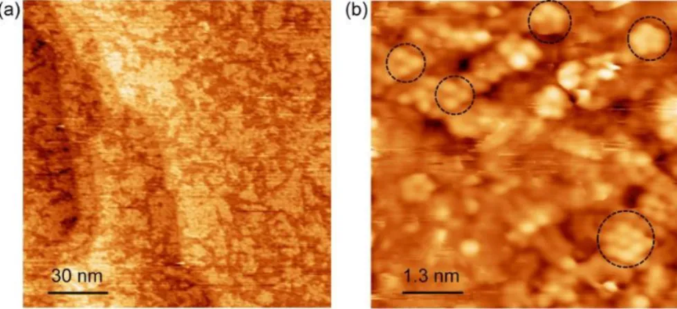
44], which adsorb on the Au(111) substrate held at room temperature. The STM images corresponding to the initial stage of phosphorus growth on Au(111) at RT are presented in figure 2. Figure 2(a) shows a large scale STM image of a phosphorus adlayer on Au(111), in which large flat Au(111) terraces covered by phosphorus clusters are observed. A magnified STM image shows a disordered phosphorus adlayer with undefined cluster geometries
occupying the terraces of the Au(111) substrate. Although the structures show no long-range order, we were able to resolve the P-clusters on the surface. The STM image shown in figure 2(b) presents the disordered phosphorus layer showing P-clusters with different geometries, including triangular, hexagonal and pentagonal shapes. Obviously, the non-periodic structure of P clusters characterized by STM is consistent with the (1 × 1) LEED pattern shown in figure 1(b).
Figure 2. STM images corresponding to phosphorus adlayer deposited on Au(111) at RT. (a) phosphorus adlayer on Au(111), revealing a rough surface morphology with high surface coverage (150 × 150 nm2, U = 1.0 V, I = 1.0 nA). (b) Atomic resolution STM image of phosphorus adlayer on Au(111) (6.5 × 6.5 nm2, U = 930 mV, I = 1.1 nA). The P-clusters of different geometrical shapes are highlighted by black dashed circles.
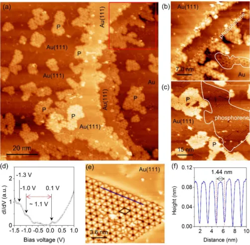
A typical STM topography, shown in figure 3(a), was recorded after post-annealing the phosphorus layer on Au(111) at 530 K. In comparison with the growth at RT (figure 2(a)), the evolution of the gold surface is completely different after post-annealing, especially at the edges of the terraces where dendritic structures have formed 2D flower-shaped nanostructures, corresponding to the triangle structure of blue phosphorene reported previously [17]. Figure 3(b) shows that the phosphorene structure not only emerges at the terrace edges but also grows within the terraces as highlighted by the white lines.
Based on the STM observation and DFT calculation, we propose that the growth process of the blue phosphorene-like structure on Au(111) starts with the substitution process. From the dendritic structures formed at the terrace edges and phosphorene structure within the terraces, we infer that the evaporated P atoms first start to replace Au atoms in the surface (substitution process) at the corners of the herringbone reconstruction where active sites are present that facilitate the ejection of the Au adatoms. It is known that the corners of the herringbone reconstruction of the Au(111) surface are preferential adsorption sites. One of the interpretations is based on exchanges at such sites [45-47]. This phenomenon has been described recently in the synthesis of borophene on the Au(111) substrate [48]. The atoms ejected from the surface subsequently diffuse either to the surface steps or form dendritic-shaped islands on the terraces as shown in figure 3(a). These Au atoms interact again with the new evaporated P atoms (substitution process) and give rise to other phosphorene islands. Note that this phenomenon was also observed during the growth of silicene on Ag(110) and Ag(111) surfaces [49-52]. Figure 3(c) reveals a second key result of the post-annealing. The islands on Au(111) surface are clearly observed with a characteristic periodic honeycomb lattice with a phosphorene-like structure. In particular, phosphorene islands can also be clearly seen within the Au terraces. A close-up STM image is shown in figure 3(e) where the phosphorene-like structure and the herringbone reconstruction of the bare Au(111) coexist on the same terrace. We characterized the electronic structure of phosphorene-like structure using STS. The dI/dV spectrum in figure 3(d), taken on the white polygon area in figure 3(c), reveals that the phosphorene-like structure within the Au(111) terrace is indeed a semiconductor. The most pronounced feature in the unoccupied state region is an asymmetric peak centered at 0.1 V. Notably, in the filled state region, the spectrum displays two clear shoulders located at −1.0 V and −1.3 V below the Fermi level. Thus, the STS investigations
give a band gap value of ~1.1 eV, in good agreement with both previous STS measurements and ARPES experiments [16-18]. Figure 3(e) reveals the finer details of the phosphorene-like structure within the Au(111) surface. A well-ordered array of bright phosphorus trimers grow within the herringbone reconstruction of Au(111). Figure 3(f) shows the line profile along the blue line of figure 3(e), indicating that the average distance between two dark centers is 1.44 nm which corresponds to five times the lattice constant of the Au(111) surface (5 × 0.288 nm = 1.44 nm), consistent with the (5 × 5) periodicity observed in LEED pattern in figure 1(c).
Figure 3. STM images of (5 × 5) phosphorene-like structure on Au(111). (a) Filled state STM image of phosphorene-like structure on Au(111) after post-annealing at 530 K for 30 min (100 × 100 nm2, U = −1.5 V, I = 0.9 nA), showing a dendritic structure at the edge of terraces. (b) Close-up STM image of the red square area in (a) (37 × 37 nm2, U = −2.0 V, I = 0.5 nA). (c) Unoccupied state STM image, showing the phosphorene-like structure islands on Au(111)
surface (74 × 74 nm2, U = 1.20 V, I = 0.80 nA). The phosphorene-like structure is highlighted by white polygon. (d) The average of STS dI/dV spectrum acquired on the phosphorene structure within the Au terrace, taken within the white polygon in (c). (e) High resolution STM image of phosphorene-like structure within the first layer of Au(111) (18 × 18 nm2, U = −480 mV, I = 1.60 nA). Unit cell of 5 × 5 blue phosphorene, highlighted by the black rhombus, includes two trimers of phosphorus atoms. (f) Profile taken along the blue line in image (e).
DFT calculations were performed first at 0 K. Following the recipe by Bernard et al [51], we calculated the difference in the formation energy between a system with a P atom adsorbed on an fcc site and that of a P atom substituting an Au surface atom, with the substituted Au atom occupying either an fcc site or along a step.
E = (EPN+1–EPN) – (EAuN+1 – EclN)
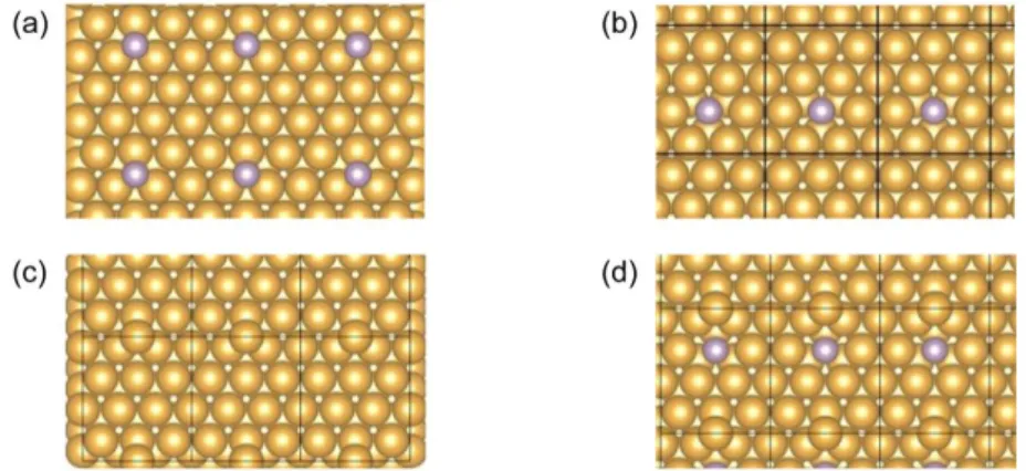
Where EPN+1, EPN, EAuN+1, EclN correspond to the total energy of: a Au(111) surface with a P
atom adsorbed on an fcc site (figure 4(a)), a P atom replacing a Au surface atom (figure 4(b)), a Au atom adsorbed on an fcc site with no P atom on the surface (figure 4(c)), and the clean Au(111) surface, respectively.
A positive energy difference would favor the substitution between a P atom and a surface Au atom, while a negative energy difference would favor a P atom adsorbed on an fcc site. The calculated energy difference for the present case is found to be −1.66 eV, strongly in favor of the adsorption of P on the Au(111) surface. However, in the case of substitution, if the adsorbed Au atom migrates to a nearby step and adsorbs along the step, this energy difference drops to −1.25 eV. In either case, it is the adsorption of a P atom that is favored, in excellent agreement with the experimental observations at the lower temperature of operation (RT).
Another way to estimate this preference is to calculate the energy difference between a system with a P atom adsorbed on an fcc site (EPN+1) and with a P atom substituting an Au atom,
where the substituted atom adsorbs on an fcc site (figure 4(d)). Again, a negative value would signal a preference for a P atom adsorbed on an fcc site (no substitution). This quantity is found to be almost the same as the one in the previous calculation, i.e. −1.64 eV vs −1.66 eV. For the calculations that follow, we adopt this definition, as only two calculations are required.
Figure 4. Configurations considered in the calculation of the total energy: (a) Au(111) surface with a P atom adsorbed on an fcc site, (b) a P atom replacing a Au surface atom, (c) a Au atom adsorbed on an fcc site with no P atom on the surface, and (d) a P atom replacing a Au surface atom with a Au atom adsorbed on a neighboring fcc site.
We have investigated in more detail the adsorption of a substituted Au atom following the surface site occupation by the P atom. We find that when the substitution takes place, the substituted Au atom stays close to the P atom on an hcp site (figure 5), with an energy difference of −0.61 eV (favoring the P atom on an fcc site, no substitution). Though this is much smaller than the −1.64 eV for the P atom on an fcc site with no substitution, it is still favored, in excellent agreement with the experimental observation. However, this new energy difference is small enough to raise the question as to what happens to the system at higher temperatures where thermal expansion induces a larger lattice constant. We have performed
the same calculations while applying a multiplication factor to the lattice constant to mimic the higher temperature. Using thermal expansion coefficient for gold of 14 × 10-6 K-1, increasing the lattice constant by a factor of 1.005 and 1.01 corresponds to 357 K and 714 K, respectively. We found that the energy difference decreased (in absolute value) to −0.54 eV, and −0.44 eV, for lattice constants of 4.19 Å, and 4.21 Å, respectively. These values show that, as the system temperature is increased, a substitution becomes more favorable, in agreement with the experiments performed at high temperatures. In these studies, we have simply adjusted the lattice constants without including any vibrational contributions to the free energy. Indeed, the vibrational energy for low coordinated atoms may become significant in determining the total free energy [53-55].
Figure 5. Au(111) surface with a Au atom adsorbed on an hcp site close to the P atom in a substitutional configuration.
To further assess the possible exchange mechanisms between an adsorbed P atom with a surface Au atom, we have considered two cases where the exchange takes place on a terrace and at a step edge. We have calculated the energetics of the Au-P exchange mechanisms for both cases. For the step edge, we used a 4 × 4 supercell with a two-row step where one of the rows is kept fixed. In figure 6, we show the initial and final configurations.
Figure 6. Au(111) surface with a P atom adsorbed on a step (grey and gold are the upper and lower Au atoms, respectively). The left panel shows the initial configuration with the P in an adatom position. The right panel shows the final substitutional configuration.
We calculated a sequence of 9 images where the first image corresponds to the P atom on the top of the step (adatom site on the surface) and the last image to the P atom incorporated in the step (surface). We used a drag method where a gold atom is pulled at a constant rate from the initial to the final configuration, with a 1D constraint along the diffusion path. In figure 7, we show the relative total energy for the exchange mechanisms by subtracting the total energy of the initial configuration. We found that for a terrace exchange, the barrier is 1.08 eV, while for a step edge we found a barrier of 0.80 eV. The difference between the two mechanisms is only 0.28 eV, pointing to the fact that both mechanisms may indeed occur albeit at different rates. These results correspond to a lattice constant of 4.17 Å (0 K). A lattice constant of 4.21 Å corresponding to an equivalent temperature of 714 K, reduces the barrier to an exchange at the terraces down to 0.97 eV, while the barrier to exchange at a step edge remains at 0.80 eV. The difference in activation energy has decreased to 0.17 eV. If we consider this in terms of a probability ratio, it is only 17:1 at 714 K, in favour of the step exchange mechanism. So both processes are likely to occur.
Figure 7. Activation energy for a P-Au exchange mechanism at a step edge and on a terrace
4. Conclusions
In summary, we have investigated the first steps of the growth of a phosphorene-like structure on the Au(111) surface at room and at elevated temperature (530 K) using LEED, AES, STM, and DFT calculations. We demonstrate that P clusters of different geometries form on Au(111) at room temperature. After post-annealing at 530 K, these clusters re-organize to form a planar hexagonal phosphorene-like structure with a (5 × 5) superstructure. We find that the evaporated P atoms react with the surface Au atoms. Under thermal activation at higher temperature, the P atoms kick out Au atoms from their surface sites (substitution process) to form the phosphorene-like structure within the top Au layer. This process does not occur at room temperature where P-clusters merely adsorb on the top Au layer. The results enable us to understand the growth behavior of blue phosphorene and demonstrate that the exchange reaction between P atoms and Au atoms should be considered.
Notes
Acknowledgements
W.Z. would like to thank the China Scholarship Council (CSC) for the PhD financial support (scholarship). AK acknowledge partial support from the US Department of Energy Basic Energy Science under Contract No DE-FG02-11ER16243. This research used resources of the National Energy Research Scientific Computing Center (NERSC), which is supported by the Office of Science of the U.S. Department of Energy.
References
[1] Novoselov K S, Mishchenko A, Carvalho A and Castro Neto A H 2016 Science 353 aac9439
[2] Appalakondaiah S, Vaitheeswaran G, Lebegue S, Christensen N E and Svane A 2012 Phys. Rev. B 86 035105
[3] Keyes R W 1953 Phys. Rev. 92 580
[4] Akahama Y, Endo S and Narita S-i 1983 J. Phys. Soc. Jpn. 52 2148
[5] Li L, Yu Y, Ye G J, Ge Q, Ou X, Wu H, Feng D, Chen X H and Zhang Y 2014 Nat. Nanotechnol. 9 372
[6] Tran V, Soklaski R, Liang Y and Yang L 2014 Phys. Rev. B 89 235319
[7] Rodin A S, Carvalho A and Castro Neto A H 2014 Phys. Rev. Lett. 112 176801 [8] Rudenko A N and Katsnelson M I 2014 Phys. Rev. B 89 201408
[9] Das S, Zhang W, Demarteau M, Hoffmann A, Dubey M and Roelofs A 2014 Nano Lett. 14 5733
[10] Liu H, Neal A T, Zhu Z, Luo Z, Xu X, Tománek D and Ye P D 2014 ACS Nano 8 4033
[11] Wang X, Jones A M, Seyler K L, Tran V, Jia Y, Zhao H, Wang H, Yang L, Xu X and Xia F 2015 Nat. Nanotechnol. 10 517
[12] Qiao J, Kong X, Hu Z-X, Yang F and Ji W 2014 Nat. Commun. 5 4475 [13] Xia F, Wang H and Jia Y 2014 Nat. Commun. 5 4458
[14] Zhu Z and Tománek D 2014 Phys. Rev. Lett. 112 176802
[15] Xu J-P, Zhang J-Q, Tian H, Xu H, Ho W and Xie M 2017 Phys. Rev. Mater. 1 061002 [16] Zhuang J, Liu C, Gao Q, Liu Y, Feng H, Xu X, Wang J, Zhao J, Dou S X, Hu Z and
Du Y 2018 ACS Nano 12 5059
[17] Zhang W, Enriquez H, Tong Y, Bendounan A, Kara A, Seitsonen A P, Mayne A J, Dujardin G and Oughaddou H 2018 Small 14 1804066
[18] Golias E, Krivenkov M, Varykhalov A, Sánchez-Barriga J and Rader O 2018 Nano Lett. 18 6672
[19] Lange S, Schmidt P and Nilges T 2007 Inorg. Chem. 46 4028
[20] Nilges T, Kersting M and Pfeifer T 2008 J. Solid State Chem. 181 1707
[21] Veselý M, Marvan P, Trejbal J i, Mazánek V, Luxa J, Šturala J i and Sofer Z k 2020 ACS Appl. Mater. Interfaces 12 22702
[22] Zhang J L, Zhao S, Telychko M, Sun S, Lian X, Su J, Tadich A, Qi D, Zhuang J and Zheng Y 2019 Nano Lett. 19 5340
[23] Han N, Gao N and Zhao J 2017 J. Phys. Chem. C 121 17893
[24] Oughaddou H, Sawaya S, Goniakowski J, Aufray B, Le Lay G, Gay J M, Tréglia G, Bibérian J P, Barrett N, Guillot C, Mayne A J and Dujardin G 2000 Phys. Rev. B 62 16653
[25] Martínez E A, Fuhr J D, Grizzi O, Sánchez E A and Cantero E D 2019 J. Phys. Chem. C 123 12910
[26] Švec M, Hapala P, Ondráček M, Merino P, Blanco-Rey M, Mutombo P, Vondráček M, Polyak Y, Cháb V, Martín Gago J A and Jelínek P 2014 Phys. Rev. B 89 201412 [27] Wang W and Uhrberg R I G 2017 Phys. Rev. Mater. 1 074002
[28] Enriquez H, Mayne A J, Kara A, Vizzini S, Roth S, Lalmi B, Seitsonen A P, Aufray B, Greber T, Belkhou R, Dujardin G and Oughaddou H 2012 Appl. Phys. Lett. 101 021605
[29] Tchalala M R, Enriquez H, Mayne A J, Kara A, Roth S, Silly M G, Bendounan A, Sirotti F, Greber T, Aufray B, Dujardin G, Ait Ali M and Oughaddou H 2013 Appl. Phys. Lett. 102 083107
[30] Gierz I, Stadtmüller B, Vuorinen J, Lindroos M, Meier F, Dil J H, Kern K and Ast C R 2010 Phys. Rev. B 81 245430
[31] Mao Y-H, Zhang L-F, Wang H-L, Shan H, Zhai X-F, Hu Z-P, Zhao A-D and Wang B 2018 Frontiers of Physics 13 138106
[32] Niu T, Zhou W, Zhou D, Hu X, Zhang S, Zhang K, Zhou M, Fuchs H and Zeng H 2019 Adv. Mater. 31 1902606
[33] Kresse G and Furthmüller J 1996 Phys. Rev. B 54 11169 [34] Kresse G and Furthmüller J 1996 Comput. Mater. Sci. 6 15 [35] Kresse G and Hafner J 1993 Phys. Rev. B 47 558
[36] Blöchl P E 1994 Phys. Rev. B 50 17953
[37] Kresse G and Joubert D 1999 Phys. Rev. B 59 1758
[38] Perdew J P, Burke K and Ernzerhof M 1996 Phys. Rev. Lett. 77 3865 [39] Yildirim H, Greber T and Kara A 2013 J. Phys. Chem. C 117 20572 [40] Hestenes M R and Stiefel E 1952 J. Res. Natl. Bur. Stand. 49 409 [41] Teter M P, Payne M C and Allan D C 1989 Phys. Rev. B 40 12255
[42] Sadeddine S, Enriquez H, Bendounan A, Das P K, Vobornik I, Kara A, Mayne A J, Sirotti F, Dujardin G and Oughaddou H 2017 Sci. Rep. 7 44400
[43] Fortin-Deschênes M, Levesque P L, Martel R and Moutanabbir O 2016 J. Phys. Chem. Lett. 7 1667
[44] Liu X, Wood J D, Chen K-S, Cho E and Hersam M C 2015 J. Phys. Chem. Lett. 6 773 [45] Biener M M, Biener J, Schalek R and Friend C M 2005 Surf. Sci. 594 221
[46] Bulou H and Massobrio C 2008 J. Phys. Chem. C 112 8743
[47] Grillo F, Früchtl H, Francis S M and Richardson N V 2011 New Journal of Physics 13 013044
[48] Kiraly B, Liu X, Wang L, Zhang Z, Mannix A J, Fisher B L, Yakobson B I, Hersam M C and Guisinger N P 2019 ACS Nano 13 3816
[49] Bernard R, Leoni T, Wilson A, Lelaidier T, Sahaf H, Moyen E, Assaud L, Santinacci L, Leroy F, Cheynis F, Ranguis A, Jamgotchian H, Becker C, Borensztein Y,
Hanbücken M, Prévot G and Masson L 2013 Phys. Rev. B 88 121411
[50] Ronci F, Serrano G, Gori P, Cricenti A and Colonna S 2014 Phys. Rev. B 89 115437 [51] Bernard R, Borensztein Y, Cruguel H, Lazzeri M and Prévot G 2015 Phys. Rev. B 92
045415
[52] Satta M, Colonna S, Flammini R, Cricenti A and Ronci F 2015 Phys. Rev. Lett. 115 026102
[53] Kara A, Durukanoglu S and Rahman T S 1996 Phys. Rev. B 53 15489 [54] Kara A, Durukanoglu S and Rahman T S 1997 J. Chem. Phys. 106 2031