HAL Id: cea-01486058
https://hal-cea.archives-ouvertes.fr/cea-01486058
Submitted on 9 Mar 2017
HAL is a multi-disciplinary open access
archive for the deposit and dissemination of
sci-entific research documents, whether they are
pub-lished or not. The documents may come from
teaching and research institutions in France or
abroad, or from public or private research centers.
L’archive ouverte pluridisciplinaire HAL, est
destinée au dépôt et à la diffusion de documents
scientifiques de niveau recherche, publiés ou non,
émanant des établissements d’enseignement et de
recherche français ou étrangers, des laboratoires
publics ou privés.
macroscopic quantum charge states
Z. Iftikhar, Sébastien Jezouin, A. Anthore, U. Gennser, F.D. Parmentier, A.
Cavanna, F. Pierre
To cite this version:
Z. Iftikhar, Sébastien Jezouin, A. Anthore, U. Gennser, F.D. Parmentier, et al.. Two-channel Kondo
effect and renormalization flow with macroscopic quantum charge states. Nature, Nature Publishing
Group, 2015, 526 (7572), pp.233 - 236. �10.1038/nature15384�. �cea-01486058�
states
Z. Iftikhar,1 S. Jezouin,1 A. Anthore,1, 2 U. Gennser,1 F.D. Parmentier,1 A. Cavanna,1 and F. Pierre1, ∗
1CNRS, Laboratoire de Photonique et de Nanostructures (LPN), 91460 Marcoussis, France 2
Univ Paris Diderot, Sorbonne Paris Cit´e, LPN, 91460 Marcoussis, France
Many-body correlations and macroscopic quantum be-haviors are fascinating condensed matter problems. A powerful test-bed for the many-body concepts and meth-ods is the Kondo model1,2 which entails the coupling of a quantum impurity to a continuum of states. It is cent-ral in highly correlated systems3–5 and can be explored with tunable nanostructures6–9. Although Kondo
phys-ics is usually associated with the hybridization of itiner-ant electrons with microscopic magnetic moments10,
the-ory predicts that it can arise whenever degenerate quantum states are coupled to a continuum4,11–14. Here we demon-strate the previously elusive ‘charge’ Kondo effect in a hybrid metal-semiconductor implementation of a single-electron transistor, with a quantum pseudospin-1/2 con-stituted by two degenerate macroscopic charge states of a metallic island11,15–20. In contrast to other Kondo nano-structures, each conduction channel connecting the island to an electrode constitutes a distinct and fully tunable Kondo channel11, thereby providing an unprecedented access to the
two-channel Kondo effect and a clear path to multi-channel Kondo physics1,4,21,22. Using a weakly coupled probe, we reveal the renormalization flow, as temperature is reduced, of two Kondo channels competing to screen the charge pseudospin. This provides a direct view of how the predicted quantum phase transition develops across the symmetric quantum critical point4,21. Detuning the pseudospin away from degeneracy, we demonstrate, on a fully characterized device, quantitative agreement with the predictions for the finite-temperature crossover from quantum criticality17.
In previous experimental investigations, the Kondo quantum impurity was of microscopic nature and mostly associated with spin6,7,9,23–25, orbital8,26, or possibly structural degrees of freedom4,27. In the ‘charge’ Kondo effect11,16,17, it is a pseudospin-1/2 constituted of two
de-generate states of a macroscopic quantum variable, the electrical charge of a metallic island comprising several billions of electrons. The role of the electrons’ spin (↑↓) in the original spin Kondo problem10 is played by the electrons’ location, in the island (↑) or elsewhere (↓). Accordingly, the charge pseudospin flips when electrons are transferred in and out of the island. The Kondo channels, each coupling the Kondo impurity (pseudo)spin with a distinct electron continuum, directly equate with the different electrical conduction channels connected to the island (distinguishing between those associated with different values of the real electron spin). In contrast,
∗e-mail: [email protected] G∞/2 G∞ a b c B 1 µm QPC2 QPCP QPC1 Vg -0.1 0.0 0.1 δVg(mV) -0.2 δVg0.0(mV) 0.2 0.00 0.25 0.50 GSET (e 2 /h ) 0.00 0.03 GSET (e 2 /h ) -200 0 200 ΔE (kB x mK) ΔE (kB x mK) -50 0 50
Figure 1. Hybrid metal-semiconductor single-electron transistor. a, Colorized picture of the sample (schematic in inset) constituted of a central metallic island (bright) connected to large electrodes (white circles) through the quantum point contacts QPC1,2 formed in a buried 2D
electron gas (darker gray). The lateral continuous gates and QPCpare used, respectively, to characterize the ‘intrinsic’ and
‘in-situ’ (renormalized) conductances of QPC1,2. The
mag-netic field B≃ 3.9 T corresponds to the integer quantum Hall regime, with the current propagating along spin-polarized edge channels (red lines) in the direction indicated by arrows. b, c, Kondo renormalized Coulomb peaks. Measured SET conductance (symbols) versus gate voltage Vg(pseudospin
en-ergy splitting ∆E), for symmetric QPC1,2 set to τ1,2≃ 0.06
(b) at T ≃ 11.5 mK or τ1,2 ≃ 0.93 (c) at T ≃ 11.5 mK (red)
and 22 mK (gray). Continuous lines are theoretical predic-tions (see main text, Methods). The agreement data-theory in c establishes the predictions for the crossover from quantum critical behavior as a function of ∆E (main text).
the electrical channels in previous Kondo nanostructures
normally merged into a single Kondo channel (except in the ingenious implementation of ref. 9), due to cooperat-ive spin-flip processes involving charge transfers between continuums. Furthermore, the charge pseudospin energy splitting, adjusted by detuning the island from degener-acy with a gate voltage, is fully equivalent to the Zeeman splitting of a magnetic Kondo impurity. Finally, of prac-tical importance, the macroscopic charge pseudospin al-lows for large channel distances, and thereby enables full and independent control as well as the in-situ character-ization of every Kondo parameter, giving access to direct comparisons with theory.
Here, we investigate a nanostructure designed to dis-play the two-channel ‘charge’ Kondo effect11,16,17. The
device (Fig. 1a) is a hybrid metal-semiconductor single-electron transistor (SET) with additional characteriza-tion probes. It essentially consists of a central metal-lic island (bright), with a continuous electronic dens-ity of states, connected to large electrodes through two quantum point contacts (QPC1,2), each tuned to a single
conduction channel. The QPCs are formed in a Ga(Al)As two-dimensional electron gas (2DEG) by field effect us-ing split gates. The 2DEG is further confined by etch-ing (to the darker gray areas), and electrically connected to the metallic island by thermal annealing. The lat-eral continuous gates are used to extract the ‘intrinsic’ transmission probabilities τ1,2 characterizing QPC1,2,
re-spectively, by short-circuiting the central island. The capacitively coupled gate voltage Vg controls the energy
difference between the island charge states. When set to weak coupling, QPCp gives us access separately to the
‘in-situ’ conductances G1,2 of QPC1,2, respectively.
Ex-cept when specifically indicated, QPCpis disconnected.
The experiment is performed down to an electronic temperature T ≃ 11.5 mK (Methods), in a perpendicular magnetic field B ≃ 3.9 T that breaks the spin degeneracy and corresponds to the integer quantum Hall effect at filling factor 2. In this regime, the current flows along two (spin-polarized) chiral edge channels. Red lines in Fig. 1a represent the outer channel, closest to the edge, with the propagation direction indicated by arrows. It is partially transmitted across QPC1,2, whereas the inner
channel (not shown) is fully reflected and can be ignored. We now review the main requirements for mapping the physics of this device to the two-channel Kondo (2CK) problem. Firstly, the typical electronic level spacing δ in the metallic island should be much smaller than the thermal energy: δ ≪ kBT , with kB the Boltzmann
constant16,17. We estimate δ ≈ k
B ×0.2 µK (Meth-ods), nearly five orders of magnitude smaller than kBT .
Secondly, the charging energy EC = e2/2C, with e the electron charge and C the overall island geometrical capa-citance, should be larger than kBT to reduce the
access-ible charge states to a pseudospin-1/2. We obtain from standard Coulomb diamond analysis EC≃kB×290 mK (Methods). Thirdly, the metallic island should be in nearly perfect contact with the 2DEG, in particular to avoid resonances involving the 2DEG-metal interface.
10-4 10-2 100 102 104 106 0.0 0.1 0.2 0.3 0.4 0.5 thy T << TK thy T >> TK GS E T (e 2 /h ) T/TK 0.0 0.2 0.4 0.6 0.8 1.0 10-8 10-6 10-4 10-2 100 Tnum K T1-τ<<1 K Tτ<<1 K TK (K ) τ a b 0.8 1.0 1.2 GS E T / G ∞ τ 11.5 22 38 80 151 0.12 0.37 0.57 0.760.93 14 T (mK )
Figure 2. Observation of the ‘charge’ Kondo effect. a, The normalized SET conductance GSET/G∞, at charge
degen-eracy (δVg= 0) and for symmetric QPC1,2, is plotted as
sym-bols versus the temperature on a log scale for different values of τ≡ τ1≃ τ2. Continuous straight lines are guides to the eye
proportional to log(T ). The grey dots are the orthogonal pro-jections of the different temperature measurements onto the plane(τ, GSET/G∞). b, The data in a at T ≤ 80 mK, rescaled
in temperature into a universal conductance curve (symbols). The violet dashed line displays the theoretical (thy) T≫ TK
prediction GSET∝ log−2(T /αTK). The red short-dashed line
displays the T≪ TKprediction e2/2h−GSET∝ T /TK
(Meth-ods). Inset, the extracted scaling parameter TK(τ) (symbols)
is compared to theoretical predictions (see Eqs. 2 and 3 for the definitions of the Kondo temperatures TKτ≪1 and TKnum,
and Methods for TK1−τ≪1).
We find that the outer edge channel is fully transmit-ted into the metallic island, with a reflection probability smaller than 0.05% (Methods). Finally, QPC1,2 should
implement point-like contacts, with a small energy de-pendence of τ1,2. For the experimental set points, we
in-crease monotonically with energy by at most 11% up to 2EC(Methods). Together, the last two tests rule out any
resonant effects.
From the influence of the charge states’ energy splitting on conductance, we observe first indications of 2CK ef-fects and establish that the measurements are performed in a regime where this physics is expected. The meas-ured conductance GSET of the QPC1-island-QPC2 SET
is shown as symbols versus gate voltage for symmetric QPCs set in the tunnel and weak-backscattering regimes, τ ≡ τ1 ≃ τ2 ≃ 0.06 (T ≃ 11.5 mK) and 0.93 (T ≃ 11.5 and 22 mK), in Fig. 1b,c respectively. The conductance exhibits periodic peaks located at successive charge de-generacy points (one full period ∆ ≃ 0.72 mV is shown in Fig. 1c, Methods).
The tunnel data in Fig. 1b are compared with the pre-diction for incoherent sequential tunneling events28
GSET= G∞ 2 2EC(δVg/∆)/kBT sinh(2EC(δVg/∆)/kBT ) , (1) with G∞ = (e 2/h)/(τ−1 1 +τ −1
2 ) the ‘classical’ SET
con-ductance and h the Plank constant. We find that the data (symbols) can be accurately reproduced with a fit temperature of 10 mK (continuous line), slightly smaller than but compatible with T ≃ 11.5 ± 1.5 mK. However, the maximum peak conductance is much higher than the standard prediction G∞/2 (dashed line), and G∞ was
left as a free fit parameter. Such an increase is expec-ted from the Kondo renormalization of the conductance, even for relatively low characteristic Kondo temperat-ure scales TK ≪ T . In this limit, Eq. 1 is predicted to provide a good approximation when substituting G∞ by
∼log−2(T /αTK), with α a numerical factor17(Methods).
Assuming τ ≪ 1, the Kondo temperature reads17:
TKτ ≪1∼ (EC/kB)exp(−π2/ √
4τ ). (2) In the opposite limit of weak-backscattering (1−τ ≪ 1), the 2CK physics is expected to be well developed. We find that the τ ≃ 0.93 data (Fig. 1c, symbols) are accur-ately reproduced, quantitatively and without fit para-meters, by the predictions (lines) from the theoretical framework where the Kondo mapping is established17
(Methods).
With these indications of 2CK effects, we now provide direct experimental evidence of Kondo physics from the temperature dependence GSET(T ) at the charge
degen-eracy point, with QPC1,2 remaining symmetric.
In standard metallic SETs, with many opaque con-duction channels, the peak conductance monotonically decreases from its high temperature classical value G∞
as the temperature is reduced29. In stark contrast, we find that GSET(δVg=0) increases as the temperature is reduced and, at T ≃ 11.5 mK, always exceeds the clas-sical conductance G∞, by up to nearly 30% (Fig. 2a).
Note that the separately characterized intrinsic energy dependencies of τ1,2 correspond to an opposite decrease
of GSET smaller than 1% for T ≲ 80 mK. Remarkably,
the conductance increase is logarithmic in T (continuous lines, for T ≲ 80 mK), which is a typical signature of the Kondo effect.
A characteristic of Kondo systems, arising from renor-malization group physics2, is that they follow
univer-sal scaling laws. We demonstrate that the conduct-ance data at T ≤ 80 mK can be rescaled into a single curve GSET(T, τ ) = GSET(T /TK), and that the
extrac-ted TK(τ ) agrees with the theoretical prediction for
the Kondo temperature (Fig. 2b). The simple rescal-ing procedure (Methods) relies on GSET overlaps for
dif-ferent τ , and on the prediction GSET(T /TK ≫ 1) ∝ log−2(T /αTK) (violet dashed line). The T ≪ TK
pre-diction e2/2h − GSET∝T /TK is displayed as a red
short-dashed line17 (Methods). The experimental scaling law covers an unprecedented range of T /TK and most of
GSET ∈ [0, 0.5]e2/h, thanks to the fully and
independ-ently tunable τ . Given the important GSET overlaps,
involving up to three successive values of τ , the rescaling accuracy provides a stringent test of the universal scal-ing law hypothesis. This conclusion is further established by confronting extracted TK(τ ) (symbols in inset) with
the predictions derived at 1 − τ ≪ 1 (Methods, red short-dashed line), τ ≪ 1 (Eq. 2, violet short-dashed line) and its generalization tested numerically (continuous line)20
TKnum∼ (EC/kB)tρ exp(−π/(4tρ)), (3)
where πtρ ≃ √
2(1 − √
1 − τ )/τ − 1. Adjusting the un-known theoretical prefactor to match TK(τ ≪ 1) or
TK(1 − τ ≪ 1), we find an overall agreement over the
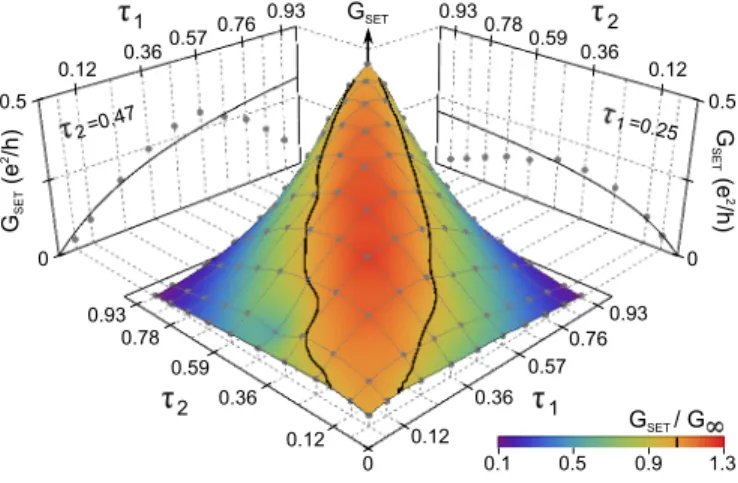
whole range τ ∈ [0, 1]. 0.1 0.5 0.9 1.3 GSET / G 1 0 0.12 0.36 0.59 0.93 0.78 0.12 0.36 0.59 0.93 0.78 0.12 0.36 0.57 0.93 0.76 0.12 0.36 0.57 0.93 0.76 0 0.5 0 0.5 GSET G SET (e 2 /h) GSET (e 2/h) 1 2 2 2=0.47 1=0.25
Figure 3. Interplay of two Kondo channels revealed by tuning the asymmetry. Main plot, the SET conductance at charge degeneracy and T= 11.5 mK is displayed (symbols) versus QPC1,2‘intrinsic’ transmission probabilities τ1,2.
Nar-row gray lines connect data points with the setting of one QPC fixed while the other is changed. The color code rep-resents GSET/G∞ (black lines indicate GSET= G∞). Lateral
panels represent the same data (symbols) for a fixed value of τ2 ≃ 0.47 (left) or τ1 ≃ 0.25 (right), together with G∞
With the ‘charge’ Kondo effect established, we turn to exploring the 2CK physics, which originates from the channels’ competition to screen the (pseudo)spin-1/2. Two symmetric Kondo channels are expected to flow, as T → 0, toward the so-called17 strong-coupling fixed
point characterized in the ‘charge’ Kondo implementa-tion by two ballistic conducimplementa-tion channels (G1,2→e2/h). In contrast to the one-channel Kondo (1CK) effect, this produces an over-screening of the pseudospin and, con-sequently, a non-Fermi liquid 2CK state with collect-ive low-energy excitations21. The 2CK state is pre-dicted to be unstable with an energy splitting of the pseudospin and with channel asymmetry, resulting in a T = 0 quantum phase transition21. Indeed, in the pres-ence of an asymmetry the most strongly coupled Kondo channel takes over, fully screening the pseudospin-1/2 at low temperatures and thereby hiding (decoupling) it from the other channel (see ref. 9 for first evidence of such a decoupling with a specific spin Kondo nanostructure30). From the quantum phase transition perspective, the 2CK non-Fermi liquid character appears as a general con-sequence of the divergent correlations near the quantum critical point (symmetric and at degeneracy)1. At finite T ≲ TK, the quantum critical (non-Fermi liquid)
beha-vior is preserved for a range of channel asymmetries and pseudospin energy splittings, which narrows down as T is reduced. Consequently, a non-Fermi to Fermi liquid crossover takes place4,21,22.
The data in symmetric QPC configurations (Fig. 1b,c, Fig. 2b) already reveal information on the 2CK phys-ics. First, the experimental scaling law (Fig. 2b) shows that two symmetric Kondo channels flow monotonic-ally toward the expected strong-coupling fixed point (2GSET ≃ G1 ≃ G2 → e2/h as T → 0). Note that for N ≥ 3 Kondo channels, the predicted symmetric fixed point is different12,17,21. In particular, for the (N = 3)-channel ‘charge’ Kondo effect, the in-situ conductance of each of the three (symmetric) QPCs is expected to flow toward 2 sin2(π/5)e2/h ≃ 0.69e2/h as T → 0, see
ref. 12. Second, the crossover from quantum critical to Fermi liquid behavior with the pseudospin energy split-ting ∆E = 2ECδVg/∆ is explored in Fig. 1c. Starting
from a well-developed 2CK state at δVg = 0 (T /TK ≈ 0.003 and 0.005), the SET conductance progressively moves away from the strong coupling fixed point e2/2h
and, at sufficiently large ∆E, decreases as the temper-ature is reduced from 22 to 11.5 mK. Remarkably, the demonstrated agreement data-theory for arbitrary δVg
validates, quantitatively, the theoretical description of the crossover17. In particular, the crossover energy scale
(such that GSET=0.5 × e2/2h) increases with T , closely following the generic expectation kBTK
√
T /TK
(Meth-ods; we are preparing a thorough study of the crossover). We provide a first evidence of the channels’ com-petition by exploring the effect of QPC asymmetry on GSET. Symbols in Fig. 3 represent GSET(τ1, τ2) meas-ured at T ≃ 11.5 mK at the charge degeneracy point, while the color code corresponds to the ratio GSET/G∞.
Note that it is only for nearly symmetric QPC1,2 that
GSET exceeds the ‘classical’ value G∞(black continuous
lines). The stronger GSET renormalization for
symmet-ric QPCs indicates that they influence each other. Strik-ingly, GSET exhibits a maximum and then decreases as
the transmission probability of one QPC is continuously increased with the other fixed (symbols in lateral pan-els). This non-monotonic behavior demonstrates that the two QPCs are not independently renormalized, and val-idates expectations for two competing Kondo channels in series17,22.
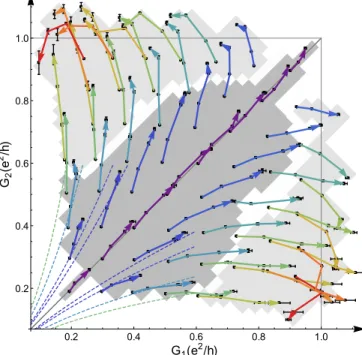
Figure 4. Two-channel renormalization flow. The ‘in-situ’ (Kondo renormalized) conductances (G1, G2) measured
at T≃ {80, 38, 22, 14} mK at charge degeneracy are displayed as symbols, with a line connecting different temperatures of a same QPC1,2 setting (characterized by the ‘intrinsic’,
un-renormalized, τ1,2), and a color code associated with∣τ1− τ2∣
(from purple for∣τ1− τ2∣ ≃ 0, to red for ∣τ1− τ2∣ ≃ 0.57). The
arrows pointing to the 14 mK conductance data points show the flow direction for decreasing temperatures. Indicative er-ror bars are obtained by repeating the measurement at sev-eral nearby charge degeneracy points. The 2CK (1CK) zone of influence is displayed as a gray (light gray) background. The conductance flows predicted at small G1,2 ≪ e2/h, for
the parameters corresponding to the crossed data line of the same color, are shown as dashed lines (Methods).
The 2CK phenomenology is directly revealed by the Kondo renormalization flow of the channels’ coupling, as temperature is reduced. It is experimentally character-ized by the (renormalcharacter-ized) ‘in-situ’ conductances G1,2.
We extract G1 and G2 separately by slightly opening
QPCp, with Gp ≪ G1,2 in order to minimize its
ef-fect (Methods). Figure 4 displays the (G1, G2) renor-malization flow for T ≃ {80, 38, 22, 14} mK. The
con-tinuous lines connect data points (symbols) obtained for identical (τ1, τ2), with an arrow indicating the flow
direc-tion and a color corresponding to ∣τ1−τ2∣(τ1,2≲0.12 and ∣τ1−τ2∣ ≳0.57 are not included due to the small signal to noise).
First, note that asymmetric G1,2 flow away from the
symmetric line, exposing plainly the development of the predicted quantum phase transition across the symmetric quantum critical point4,17,21,22. Second, the
renormaliz-ation flow also displays the predicted crossover from 2CK to 1CK behavior. The 2CK zone of influence, shown as a gray background in Fig. 4, is characterized by an in-crease of both G1 and G2 as T is reduced. This occurs
for G1,2≲0.5e2/h (that is, T ≲ TK) or for relatively sym-metric G1,2. The 1CK zone of influence, shown as a light
gray background in Fig. 4, is characterized by the reduc-tion of the smallest ‘in-situ’ conductance as T is lowered, while the largest further increases until reaching ∼ e2/h. This occurs for asymmetric G1,2 and only if the largest
‘in-situ’ conductance is above ∼ 0.5e2/h, corresponding to
an important screening of the pseudospin. Note that the
limit of one perfectly ballistic QPC was previously invest-igated in the context of dynamical Coulomb blockade31. Further information are disclosed by the experimental renormalization flow, including the temperature evolu-tion of channel asymmetry. Intriguingly, we also ob-serve (Fig. 4) that the ‘in-situ’ conductance of the most strongly coupled QPC can slightly overstep the standard quantum limit e2/h. This overshoot is robust to exper-imental conditions, above noise level and not a simple calibration artifact (Methods).
The present observation of the two-channel ‘charge’ Kondo effect demonstrates that Kondo physics applies to the degenerate macroscopic quantum states of electrical circuits. Our hybrid device allows full control and char-acterization of the Kondo parameters, and gives access to (N ≥ 2)-channel Kondo physics. The implementation in the quantum Hall regime also opens the path to ex-ploring the Kondo physics with anyonic quasiparticles, at fractional filling factors. One limitation is the smallness of the charging energy EC. However, we anticipate that
much higher EC are feasible by replacing the buried 2D
electron gas with a surface conductor, such as graphene.
[1] Vojta, M. Impurity quantum phase transitions. Phil. Mag. 86, 1807–1846 (2006).
[2] Bulla, R., Costi, T. A. & Pruschke, T. Numerical renor-malization group method for quantum impurity systems. Rev. Mod. Phys. 80, 395–450 (2008).
[3] Hewson, A. C. The Kondo problem to heavy fermions (Cambridge Univ. Press, 1997).
[4] Cox, D. L. & Zawadowski, A. Exotic Kondo effects in metals: Magnetic ions in a crystalline electric field and tunnelling centres. Adv. Phys. 47, 599–942 (1998). [5] Dzero, M., Sun, K., Galitski, V. & Coleman, P.
Topo-logical Kondo Insulators. Phys. Rev. Lett. 104, 106408 (2010).
[6] Goldhaber-Gordon, D. et al. Kondo effect in a single-electron transistor. Nature 391, 156–159 (1998). [7] Cronenwett, S. M., Oosterkamp, T. H. & Kouwenhoven,
L. P. A Tunable Kondo Effect in Quantum Dots. Science 281, 540–544 (1998).
[8] Sasaki, S., Amaha, S., Asakawa, N., Eto, M. & Tarucha, S. Enhanced Kondo Effect via Tuned Orbital Degeneracy in a Spin 1/2 Artificial Atom. Phys. Rev. Lett. 93, 017205 (2004).
[9] Potok, R. M., Rau, I. G., Shtrikman, H., Oreg, Y. & Goldhaber-Gordon, D. Observation of the two-channel Kondo effect. Nature 446, 167–171 (2007).
[10] Kondo, J. Resistance minimum in dilute magnetic alloys. Prog. Theor. Phys. 32, 37–49 (1964).
[11] Matveev, K. A. Quantum fluctuations of the charge of a metal particle under the Coulomb blockade conditions. Sov. Phys. JETP 72, 892–899 (1991).
[12] Yi, H. & Kane, C. L. Quantum Brownian motion in a periodic potential and the multichannel Kondo problem. Phys. Rev. B 57, R5579–R5582 (1998).
[13] Le Hur, K. Kondo resonance of a microwave photon. Phys. Rev. B 85, 140506 (2012).
[14] Goldstein, M., Devoret, M. H., Houzet, M. & Glaz-man, L. I. Inelastic Microwave Photon Scattering off a Quantum Impurity in a Josephson-Junction Array. Phys. Rev. Lett. 110, 017002 (2013).
[15] Glazman, L. I. & Matveev, K. A. Lifting of the Coulomb blockade of one-electron tunneling by quantum fluctu-ations. Sov. Phys. JETP 71, 1031–1037 (1990). [16] Matveev, K. A. Coulomb blockade at almost perfect
transmission. Phys. Rev. B 51, 1743–1751 (1995). [17] Furusaki, A. & Matveev, K. A. Theory of strong inelastic
cotunneling. Phys. Rev. B 52, 16676–16695 (1995). [18] Zar´and, G., Zim´anyi, G. T. & Wilhelm, F.
Two-channel versus infinite-Two-channel Kondo models for the single-electron transistor. Phys. Rev. B 62, 8137–8143 (2000).
[19] Le Hur, K. & Seelig, G. Capacitance of a quantum dot from the channel-anisotropic two-channel Kondo model. Phys. Rev. B 65, 165338 (2002).
[20] Lebanon, E., Schiller, A. & Anders, F. B. Coulomb block-ade in quantum boxes. Phys. Rev. B 68, 041311 (2003). [21] Nozi`eres, P. & Blandin, A. Kondo effect in real metals.
J. Phys. 41, 193–211 (1980).
[22] Pustilnik, M., Borda, L., Glazman, L. I. & von Delft, J. Quantum phase transition in a two-channel-Kondo quantum dot device. Phys. Rev. B 69, 115316 (2004). [23] Nygard, J., Cobden, D. H. & Lindelof, P. E. Kondo
phys-ics in carbon nanotubes. Nature 408, 342–346 (2000). [24] Park, J. et al. Coulomb blockade and the Kondo effect
in single-atom transistors. Nature 417, 722–725 (2002). [25] Liang, W., Shores, M. P., Bockrath, M., Long, J. R. &
Park, H. Kondo resonance in a single-molecule transistor. Nature 417, 725–729 (2002).
[26] Jarillo-Herrero, P. et al. Orbital Kondo effect in carbon nanotubes. Nature 434, 484–488 (2005).
Buhr-man, R. A. 2-channel Kondo scaling in conductance sig-nals from 2 level tunneling systems. Phys. Rev. Lett. 72, 1064–1067 (1994).
[28] Beenakker, C. W. J. Theory of Coulomb-blockade oscil-lations in the conductance of a quantum dot. Phys. Rev. B 44, 1646–1656 (1991).
[29] Joyez, P., Bouchiat, V., Esteve, D., Urbina, C. & Devoret, M. H. Strong Tunneling in the Single-Electron Transistor. Phys. Rev. Lett. 79, 1349–1352 (1997). [30] Oreg, Y. & Goldhaber-Gordon, D. Two-Channel Kondo
Effect in a Modified Single Electron Transistor. Phys. Rev. Lett. 90, 136602 (2003).
[31] Jezouin, S. et al. Tomonaga-Luttinger physics in elec-tronic quantum circuits. Nat. Comm. 4, 1802 (2013). Acknowledgments. This work was supported by the ERC (ERC-2010-StG-20091028, #259033) and the French REN-ATECH network. We gratefully acknowledge E. Boulat, J. von Delft, S. De Franceschi, L. Glazman, D. Goldhaber-Gordon, K. Le Hur, A. Keller, K. Matveev, L. Peeters, P. Si-mon and G. Zar´and for the critical reading of our manuscript and discussions.
Author Contributions. Z.I. and F.P. performed the ex-periment. Z.I., A.A. and F.P. analyzed the data. F.D.P. fabricated the sample. U.G. and A.C. grew the 2DEG. S.J. contributed to a preliminary experiment. F.P. led the project and wrote the manuscript with inputs from Z.I., A.A. and U.G.
Author Information. Reprints and permissions informa-tion is available at www.nature.com/reprints. The authors declare no competing financial interests. Correspondence and requests for materials should be addressed to F.P. ([email protected]).
METHODS
Experimental setup. The measurements were performed using standard lock-in techniques, at frequencies below 100 Hz, in a dilution refrigerator. Multiple filters along the electrical lines and two shields at the mixing chamber protect the sample from spurious high energy photons.
Sample. The sample is nanostructured by standard e-beam lithography in a 70 nm deep GaAs/Ga(Al)As two-dimensional electron gas of density 2.5× 1011 cm−2 and mo-bility 106 cm2V−1s−1. The metallic island is constituted of nickel (30 nm), germanium (60 nm) and gold (120 nm). Electronic temperature. The electronic temperature T and the associated error bars are obtained from standard quantum shot noise measurements across both QPC1,2 and,
at T ≥ 38 mK, also from the readings of a RuO2
thermo-meter. The temperature stability is ascertained by measuring the electronic temperature before and after data acquisition, as well as with continuous RuO2 readings. For details on the
noise measurement setup see the supplementary materials of ref. 32.
Electronic level spacing in the metallic island. The typical energy spacing between electronic levels in the cent-ral metallic island is evaluated from the standard expression δ = 1/(νFΩ), with Ω the island’s volume and νF the
elec-tronic density of states per unit volume and energy in the metallic island. Injecting the island’s volume Ω≃ 3 µm3 and a typical density of states for metals νF ≈ 1047 J−1m−3 (in
gold, the main constituent, νF ≃ 1.14 × 1047J−1m−3), we find
δ ≈ kB× 0.2 µK ⋘ kBT . The very small electronic level
spacing, more than four orders of magnitude smaller than the thermal energy kBT , verifies the essential hypothesis δ≪ kBT
in the theory11,16,17. To further demonstrate that, in gen-eral, the electronic level spacing in the island is fully neg-ligible, one can compare δ with the electronic level energy width h/τφ, where τφ is the electronic quantum coherence
time. Indeed, δ ≪ h/τφ corresponds to a continuous
elec-tronic density of states. The typical electron quantum coher-ence time is in the 10 ns range at low temperatures in similar diffusive metals33 (see e.g. ref. 34 for the measurement of τφin gold). The corresponding electronic level energy width
h/τφ∼ kB× 5 mK ⋙ δ is therefore greater than the typical
level spacing by approximately four orders of magnitude. Interface metallic island - 2D electron gas. It is crucial to achieve a nearly perfect transmission of the outer electronic channel propagating along the edge of the buried 2DEG to-ward the central metallic island. Here, we detail the proced-ure to precisely determine this transmission probability. The notations are recapitulated in Extended Data Figure 1. In the following, the lateral gates are fully depleted. First, QPC1,2,p
are set to the middle of the very flat and large (∼ 0.4 V) inter-mediate plateau at τ1,2,p= 1 (thanks to the robust quantum
Hall effect, see Extended Data Fig. 2c for the corresponding plateau across a lateral characterization gate) and we measure the corresponding Vτ1,2,p=1
ii (i∈ {1, 2, p}). The transmission
probability τΩ−iof the outer edge channel from QPCiinto the
metallic island is then given by the expression
Vτ1,2,p=1
ii = (2 − τΩ−i)Vi/2 + τΩ−i
τΩ−iVi/2
τΩ−1+ τΩ−2+ τΩ−p.
Note that we made absolutely sure there are no other ways than through the metallic island to go from QPCi to QPCj,
with i≠ j. This is done by etching trenches in the 2DEG un-derneath the island (see Fig. 1a and Extended Data Fig. 1).
Second, we eliminate calibration uncertainties by measuring the reflected signals Vτ1,2,p=0
ii = Viwith QPC1,2,pdisconnected
(depleted). The ratios Vτ1,2,p=1
ii /V
τ1,2,p=0
ii give τΩ−i
independ-ently of the injection and measurement chains calibrations:
Vτ1,2,p=1
ii
Vτ1,2,p=0
ii
= (2 − τΩ−i)/2 + τΩ−i τΩ−i/2
τΩ−1+ τΩ−2+ τΩ−p. (4)
With this approach, we obtain∣1 − τΩ−i∣ ≲ 3 × 10⁻⁴: τΩ−1= 0.9997, τΩ−2= 1.0003, τΩ−p= 1.0001.
The outer edge channel is perfectly transmitted into the metallic island at our experimental accuracy.
Calibration of injection and measurement chains. In the same spirit as above, and now assuming τΩ−i= 1, we
nor-malize the signal Vij (see notations in Extended Data Fig. 1)
by the signal Vijτi,j(k)=1(0)measured when setting τi,j= 1 with
the other QPC disconnected, τk= 0. For i ≠ j, this gives
vij≡ Vij/V τi,j(k)=1(0) ij = GiGj2h/e2 G1+ G2+ Gp . (5) The same information can also be extracted by solving the set of three equations for the reflected signals (i= j)
vii≡ Vii/V τ1,2,p=0 ii = (1 − Gih/2e2) + G2 ih/2e2 G1+ G2+ Gp . (6) Note that if Gp= 0, the measurements of v11, v22, v12and v21
are redundant and only give access to GSET= 1/(G−11 + G−12 ),
but not to G1and G2 separately.
Quantum point contacts characterization. Extended Data Fig. 2a(b) displays as a continuous line the measured ‘in-trinsic’ (not renormalized by Kondo effect or Coulomb block-ade) transmission probability τ1(2)of QPC1(2)versus the gate voltage Vqpc1(2)applied to one side of the corresponding split gate (T ≃ 11.5 mK, no dc bias voltage). The symbols indic-ate the QPC set points used in the experiment. Note that for larger (less negative) values of Vqpc1,2, the ‘intrinsic’ quantum
point contact conductances exhibit a wide (∼ 0.4V) plateau, precisely at e2/h and robust to dc voltages within the ex-plored range ∣Vdc∣ < 100 µV. This is followed by a second
step up to 2e2/h corresponding to the opening of a second
electronic (inner edge) channel (not shown but similar to the lateral characterization gate, see Extended Data Fig. 2c). The insets in Extended Data Fig. 2a,b show the relative variation of the corresponding ‘intrinsic’ QPC differential conductance with the applied dc bias voltage, up to∣Vdc∣ = 50 µV ≃ 2EC/e
and for τ1,2≃ {0.06, 0.47, 0.93} (data shifted vertically by 0.1
for clarity). The relatively small impact of dc bias voltage corroborates a point-like description of the quantum point contacts within the pertinent energy range, below EC. Note
that the broad dip visible in the transmission across QPC1at
larger split gate voltages Vqpc1 (Extended Data Fig. 2a) has
no impact at the used experimental set points. In particular, it does not result in strongly energy dependent transmission probabilities (inset of Extended Data Fig. 2a and Extended Data Fig. 2e) and it has no impact on the dynamical Coulomb blockade low bias conductance suppression (Extended Data Fig. 2d). To perform the measurements in Extended Data Fig. 2a,b, both lateral characterization gates (Fig. 1a, color-ized yellow for QPC2, not colorized for QPC1) were set to zero
gate voltage. As shown Extended Data Fig. 2c, this corres-ponds to fully transmitting the two electronic edge channels
across the lateral gates, thereby effectively short-circuiting the central metallic island (in normal operations the lateral char-acterization gates are set to≈ −0.4 V in order to deplete the 2DEG underneath, for further details regarding the lateral characterization gates ‘switch’ operation see the supplement-ary information in ref. 35). Extended Data Fig. 2d shows as continuous lines the differential conductance across QPC1,2
measured at 22 mK as a function of dc voltage with the nearby lateral characterization gate set to deplete the 2DEG (biased at ≈ −0.4 V, as when exploring the 2CK physics) while the lateral gate on the opposite side of the metallic island is set to transmit the two edge channels (biased at≈ 0 V), as il-lustrated schematically. The central conductance dip at low dc voltage corresponds to the dynamical Coulomb blockade suppression of the conductance31,35, while the flat plateaus
at large dc voltages are used to extract the ‘intrinsic’ trans-mission probabilities τ1,2 here displayed as horizontal dashed
lines. The precise values of the ‘intrinsic’ transmission prob-abilities τ1,2at the experimental set points, and their relative
increase ∆τ1,2/τ1,2 between zero bias and ±50 µV
(corres-ponding to our estimated experimental uncertainty on τ ), are recapitulated in Extended Data Fig. 2e.
Capacitive cross-talk. Changing the gate voltage con-trolling one QPC also slightly affects the other ones. This cross-talk is determined precisely using the lateral character-ization gates, from the shift in gate voltage of the QPC ‘in-trinsic’ conductance curves shown Extended Data Fig. 2a,b. Thanks to the relatively important distances (several micro-meters) between QPCs (compared to small quantum dots) the cross-talk correction is small, typically a few percent. We take into account the small capacitive cross-talk correction during data acquisition.
Charging energy characterization. The charging energy EC = e2/2C ≃ kB× 290 mK is obtained from the measured
Coulomb diamonds displayed Extended Data Fig. 3.
Conductance peak reproducibility. Although a single period of GSET(Vg) is shown Fig. 1c, we systematically
meas-ured several nearby periods for each configuration. Extended Data Fig. 4 displays as symbols several consecutive periods measured at base temperature T = 11.5 mK for the same configuration τ = 0.93 shown in Fig. 1c, together with the quantitative theoretical prediction of Eq. 9 (continuous line). In practice we take the average of the maximum conductance (at charge degeneracy) measured for different periods, and we estimate the experimental uncertainty (s.e.m.) from the the scatter between values. For some relatively rare combina-tions of QPC settings, temperatures and precise gate voltages, we find anomalously small values of the maximum conduct-ance with respect to the overall experimental standard de-viation. We systematically eliminate such anomalous data points, which can often be attributed to charge jumps in the sample vicinity, by considering only the data within a win-dow of four times the overall experimental standard deviation. This automatic procedure removes approximately 10% of the measured local conductance maximums. In Figs. 2,3, the ex-tracted uncertainty (not shown) is smaller than the symbols. In Fig. 4, the extracted experimental uncertainty is displayed as error bars.
Theoretical expression of GSET and G1,2 at τ1,2 ≪ 1
(T ≫ TK). In the limit T ≫ TK (also corresponding to the
tunnel regime τ1,2 ≪ 1) the two Kondo channels are
inde-pendent from one another since they only weakly screen the pseudospin-1/2. Consequently the ‘in-situ’ (Kondo renormal-ized) conductances G1,2 ≪ e2/h renormalize independently,
increasing as temperature is reduced near charge degener-acy (δVg ≈ 0) due to the Kondo effect. Theory predicts that
the standard expression Eq. 1 for independent sequential tun-neling events holds provided that the ‘intrinsic’ transmission probabilities τ1,2 in G∞= (e2/h)/(τ1−1+ τ2−1) are substituted
by the Kondo renormalized values17 τ1,2→ π
2
/ log2
(max{T, 2EC∣δVg/∆∣/kB}/αTK1,2), (7)
where α is a numerical factor depending on the precise defin-ition of TK1,2 = TK(τ1,2) (Eq. 2, see ‘Rescaling procedure’
below for the determination of α). Note that the substitution Eq. 7 leaves the width of the conductance line shape essen-tially proportional to temperature, although slightly narrower in reasonable agreement with the data. Consequently, at a good approximation in the tunnel regime, the Kondo effect essentially results in an increased value of the parameter G∞
in Eq. 1. In this spirit, we have fitted the tunnel data shown Fig. 1b (symbols) using Eq. 1 with the temperature and G∞
as free parameters (continuous line). In Fig. 2b, at charge degeneracy (δVg= 0), the displayed theoretical (thy) T >> TK
prediction (violet dashed line) is given by
Gthy T/TK≫1 SET (T /TK) = 9.62 e2 h log −2( T 0.0037TK) . (8) In Fig. 4, the displayed predictions for the renormalization flow at small G1,2≲ 0.6e2/h (dashed lines with the same color
code as the corresponding data) are calculated without ad-ditional fit parameters, using G1,2= 2Gthy TSET /TK≫1(T /TK1,2),
with TK1,2 = TK(τ = τ1,2) given by the previously
extrac-ted experimental scaling temperature shown in the inset of Fig. 2b, and with Gthy T/TK≫1
SET given by Eq. 8.
Theoretical expression of GSET at τ1,2≈ 1. The
quant-itative expression of GSET has been established for
arbit-rary offsets from the charge degeneracy point (δVg), in the
limit where both QPC1,2 are set close to the ballistic limit
(1− τ1,2 ≪ 1) and for low temperatures with respect to the
charging energy kBT ≪ EC (ref. 17, based on the
theoret-ical framework developed in ref. 16). The prediction shown as a continuous line in Fig. 1c is obtained quantitatively, without fit parameters, from the following theoretical expres-sion (Eqs. 38, 26 and A9 in ref. 17):
GSET= e2 2h[1 − π3γΓ+kBT 16EC − ∫ ∞ 0 Γ2−/ cosh2(x) (xπ2k BT/γEC)2+ Γ2−dx], (9) with γ≃ exp(0.5772) and
Γ±= 2 − τ1− τ2± 2
√
(1 − τ1)(1 − τ2) cos(2πδVg/∆).
Note that we have supplemented Eq. 38 of ref. 17 with the small correction proportional to kBT/ECin Eq. A9, following
the same procedure used in Fig. 2 of ref. 17. The function Γ−
reduces to zero when the sample is set to display the 2CK effect (τ1= τ2 and δVg = 0). Instead, the integral term with
Γ− in Eq. 9 determines the crossover from quantum critical-ity, as further discussed in the next section. In symmetric situations (τ1 = τ2) and at the degeneracy point (δVg = 0),
all the temperature dependence describing the flow toward the 2CK state (quantum critical point) results from the term proportional to Γ+ in Eq. 9. Without additional hypothesis than τ≡ τ1= τ2 and δVg= 0, Eq. 9 can be reformulated as a
universal scaling function, whose value tends linearly toward
the quantum critical point e2/2h when the temperature goes to 0: GT≪TK SET (T /T 1−τ≪1 K , δVg= 0) = e2 2h(1 − T /2T 1−τ≪1 K ) , (10)
with the Kondo scaling temperature defined as TK1−τ≪1=
2EC
π3γk B(1 − τ)
. (11)
Note that although for small enough 1− τ the Kondo tem-perature can become larger than the charging energy EC, the
latter remains a high energy cutoff for the Kondo physics since at larger energies (e.g. kBT ≳ EC) additional charge
states of the island become accessible. Note also that equally valid definitions of the Kondo temperature can differ by a con-stant multiplicative factor: replacing T/2TK1−τ≪1in Eq. 10 by
αT/2TK1−τ≪1 would change the expression of TK1−τ≪1 by the
multiplicative factor α. Here, the definition of TK1−τ≪1 was
chosen such that GT≪TK
SET (T = T 1−τ≪1
K , δVg = 0) = 0.5 × e2/2h
(although T = TK1−τ≪1 is beyond the range of validity of
Eq. 10). The red short-dashed line displayed in the main panel of Fig. 2b is the quantitative prediction for GSET(T )
calculated with Eq. 10 for τ= 0.86 and EC = kB× 290 mK.
It was rescaled in T/TK using the same experimental scaling
temperature TK(τ = 0.86) ≃ 1.4 K as the τ = 0.86 data (and
not TK1−τ≪1(τ = 0.86) ≃ 0.075 K) to allow a direct comparison
data/theory in Fig. 2b. In the inset of Fig. 2b, a constant multiplicative factor is applied to TK1−τ≪1 ∝ 1/(1 − τ) (red
short-dashed line) to match the experimental scaling temper-ature at τ≈ 1.
Predictions for the crossover from quantum critical-ity. In this section, we show that the predictions of Eq. 9 correspond to generic expectations for the crossover from quantum criticality4,22,36. An asymmetry between Kondo channels (τ1− τ2≠ 0) or a lifting of the charge pseudospin
de-generacy (δVg ≠ 0) is predicted to destroy the unstable 2CK
state at vanishing temperatures; and a crossover from non-Fermi liquid (quantum critical) to non-Fermi liquid behavior is expected to take place as temperature is reduced. The corres-ponding crossover temperature is generically expected4,22,36 to depend quadratically on the strength of the perturbations near the symmetric (τ1= τ2, δVg= 0) quantum critical point.
The theoretical prediction of Eq. 9 describes quantitatively the crossover from quantum criticality for the present two-channel ‘charge’ Kondo effect, in the presence of an asym-metry between the two channels and/or of a pseudospin en-ergy splitting. As generically expected, Eq. 9 predicts that any perturbation (τ1 ≠ τ2 and/or δVg ≠ 0) results in a
SET conductance vanishing in the low temperature limit as T2, the standard Fermi-liquid power law (see also Eq. 39 in ref. 17). The crossover behavior is described by a single function, independent of the perturbations (channel asym-metry δτ = τ1 − τ2, energy splitting ∆E = 2ECδVg/∆, or
both simultaneously) that are encapsulated in the parameter Γ−, thereby corroborating the universal behavior put forward in ref. 36. The crossover temperature Tco can be
extrac-ted from Eq. 9. Here it is defined as the temperature at which GSET = 0.5 × e2/2h (assuming a fully developed 2CK
state in absence of perturbation, ie neglecting the term pro-portional to Γ+T/EC in Eq. 9). At δVg = 0 and for small
δτ≪ 2 − τ1− τ2, one obtains from Eq. 9 the crossover
temper-ature Tco(∆E = 0, δτ) ≃ (γ2π/4)TK1−τ≪1(δτ) 2
, corresponding to generic predictions (detailed in e.g. ref. 36). At δτ= 0 and
for small δVg≪ ∆, one obtains from Eq. 9 the crossover
tem-perature Tco(∆E, δτ = 0) ≃ (4/π3)TK1−τ≪1(∆E/kBTK1−τ≪1)2,
corresponding to generic predictions36.
Rescaling procedure. We show Fig. 2b that the data GSET(T, τ) for symmetric QPCs (τ ≃ τ1 ≃ τ2) can be
res-caled into a single curve GSET(T /TK). To illustrate the
pro-cedure let us consider two successive transmissions τ and τ′ with a conductance overlap such that one can find two data points GSET(T, τ) = GSET(T′, τ′). The existence of a
univer-sal scaling law directly implies TK(τ′)/TK(τ) = T′/T . If such
a law exists, then the rescaled data at τ and τ′should match on the full range of conductance overlap. This scheme does not apply directly for the three lowest transmission probabil-ities τ ≃ {0.06, 0.125, 0.245}, since there is no conductance overlap. However, theory predicts17 in the corresponding
limit T ≫ TK that GSET(T ) ∝ log−2(T /αTK). Using this
expression to fit and extrapolate the τ < 0.25 data points (dashed line in Fig. 2b), we can apply the above procedure. Note that TK(τ) is extracted only up to an overall prefactor.
Following standard usage37, we set this prefactor such that GSET(T /TK = 1) = 0.5 × e2/2h (half the 2CK state
conduct-ance).
Absence of numerical renormalization group calcula-tions for GSET(T/TK). To the best of our knowledge, there
are no available numerical calculations for the measured con-ductance GSET. Consequently, there is no theoretical
pre-diction to compare with the experimentally extracted scaling curve GSET(T /TK) shown Fig. 2b, beyond the limits of large
or small T/TK. Quoting the authors of ref. 22, the root of
the difficulty “is that there is no mapping between the con-ductance across the island (GSET) and the electron
scatter-ing cross-section in the generic two-channel Kondo model”. Hopefully, future numerical works, adapted to the present charge Kondo implementation, will fill this gap and allow a full quantitative comparison data-theory, including at inter-mediate values of T/TK.
Extracting separately the ‘in-situ’ conductances G1
and G2 with QPCp. The SET conductance, with QPCp
disconnected, only gives access to the series combination of the ‘in-situ’ (Kondo renormalized) conductances G1 and G2
(GSET= 1/(G−11 +G−12 )). This is sufficient in symmetric
config-urations G1≃ G2, but not to extract the full renormalization
flow shown in Fig. 4. For this purpose we use an additional probe QPCp. To minimize the effect of this probe, it is set to a
relatively small coupling with respect to G1 and G2. In
prac-tice, 1/150 < Gp/min(G1, G2) < 1/6, with the largest values
corresponding to the most asymmetric configurations between QPC1,2. As easily checked from Eq. 5, this gives access
dir-ectly to G1/G2 = vp1/vp2 (or equivalently, G1/G2= v1p/v2p).
Solving Eqs. 5 and 6, with the measured vij gives all three
‘in-situ’ conductances G1,2,p(provided that G1,2,p≠ 0).
‘In-situ’ conductances above the standard quantum limit e2/h. Some of the ‘in-situ’ conductances displayed Fig. 4 slightly overstep the standard quantum limit e2/h for
asymmetric QPCs configurations and at low temperatures. Although the standard quantum limit applies to a single quantum channel connected to voltage biased reservoirs (in contrast, the central metallic island is floating) and in the absence of interactions, to the best of our knowledge such a striking behavior was never observed. In principle, a par-tial transmission of the second (inner) edge channel across the QPC could provide a simple explanation for the observa-tion of an in-situ conductance above e2/h. However this is unlikely since the second electronic channel is initially com-pletely reflected, separated from the full opening of the first
(outer) channel by a plateau very wide and very robust to dc voltage (tested up to∣Vdc∣ ≃ 100 µV ≈ 4EC/e). Note that
we checked in-situ that the lateral characterization gates set to reflect the two edge channels (τlcg= 0, at Vlcg≈ −0.4 V),
as well as QPCp when initially disconnected, remain in this
configuration in presence of the charge Kondo effect. It is also noteworthy that in the present experimental configur-ation, in the integer quantum Hall regime at filling factor ν= 2, the current between the metallic island and the QPCs is carried by two copropagating quantum Hall channels that are coupled by the Coulomb interaction. However, for the short distance island-QPC and very low temperatures in the present experimental investigation, this coupling is expected to be negligible38. A similar transient overshoot is predicted in the related Luttinger liquid problem (at K< 1/2, see Fig. 1 in ref. 39), which corresponds to an ‘in-situ’ single channel differential conductance above e2/h (in the context of the Lut-tinger liquid-dynamical Coulomb blockade mapping31,40).
We here show that our intriguing observation is well above the noise level, that the same result is obtained with differ-ent sets of measuremdiffer-ents, and that it is robust with respect to injection voltage and to the coupling of QPCp. For this
purpose we focus on the set point (τ1 = 0.76, τ2 = 0.93) at
T ≃ 14 mK. Extended Data Fig. 5a,b,c,d show the normal-ized transmitted signals vij with i≠ j and the reflected
sig-nal 2− vpp, measured in the linear response regime with here
Vi≃ 1.15 µVrms< kBT/e. The displayed statistical error bars
are here obtained by repeating the measurements ten times in a row for each data point. Possible charge offsets jumps are ruled out from the reproducibility of the two displayed consecutive sweeps (Vg increasing and decreasing). Note that
the same normalized data are found for the reciprocal signals vij≃ vji. Note also that QPCp is here set to a different
tun-ing (with a higher conductance) than the correspondtun-ing data point in Fig. 4. First, we extract G1,2,p solving Eq. 5 with
only the transmitted signals (vij with j ≠ i). Averaging all
the data (Vgincreasing and decreasing, and reciprocal signals)
at the degeneracy point, we find G1= 0.508 ± 0.003 e
2
/h, G2= 1.11 ± 0.02 e2/h,
Gp= 0.0387 ± 0.0005 e2/h.
Second, we show that the same result is obtained with a dif-ferent set of measurements, now involving also Eq. 6. We use v12/2 and 2(1 − vpp) (Extended Data Fig. 5d) corresponding
to 1/(G−11 +G−12 ) and Gp, respectively, in the limit Gp≪ G1,2,
as well as v1p/v2p= G1/G2Extended Data Fig. 5e). This gives
the consistent values
G1= 0.510 ± 0.002 e2/h,
G2= 1.107 ± 0.006 e2/h,
Gp= 0.0395 ± 0.0002 e2/h.
In fact, no averaging is required to show that G2 > e2/h
well beyond the noise level. Focusing on the smallest sig-nal v1p/v2p = G1/G2, we observe directly in Extended Data
Fig. 5e that every data point near δVg ≈ 0 is below the red
line displaying the ratio for which G2 = e2/h. Every data
point therefore corresponds to G2> e2/h. To further confirm
G2 > e2/h, we have also checked that this observation is
ro-bust with respect to injection voltage Vi and to the value of
[32] Jezouin, S. et al. Quantum Limit of Heat Flow Across a Single Electronic Channel. Science 342, 601–604 (2013). [33] Pierre, F. et al. Dephasing of electrons in mesoscopic
metal wires. Phys. Rev. B 68, 085413 (2003).
[34] Wellstood, F. C., Urbina, C. & Clarke, J. Hot-electron effects in metals. Phys. Rev. B 49, 5942–5955 (1994). [35] Parmentier, F. D. et al. Strong back-action of a linear
circuit on a single electronic quantum channel. Nat. Phys. 7, 935–938 (2011).
[36] Sela, E., Mitchell, A. K. & Fritz, L. Exact Crossover Green Function in the Two-Channel and Two-Impurity Kondo Models. Phys. Rev. Lett. 106, 147202 (2011). [37] Goldhaber-Gordon, D. et al. From the Kondo Regime
to the Mixed-Valence Regime in a Single-Electron Tran-sistor. Phys. Rev. Lett. 81, 5225–5228 (1998).
[38] le Sueur, H. et al. Energy Relaxation in the Integer Quantum Hall Regime. Phys. Rev. Lett. 105, 056803 (2010).
[39] Fendley, P., Ludwig, A. W. W. & Saleur, H. Ex-act nonequilibrium transport through point contEx-acts in quantum wires and fractional quantum Hall devices. Phys. Rev. B 52, 8934–8950 (1995).
[40] Safi, I. & Saleur, H. One-Channel Conductor in an Ohmic Environment: Mapping to a Tomonaga-Luttinger Liquid and Full Counting Statistics. Phys. Rev. Lett. 93, 126602 (2004).
QPC
2QPC
PQPC
1V
1V
2V
pV
11V
12V
1pV
21V
22V
2pV
p1V
p2V
ppp
1
2
Extended Data Figure 1. Measurement schematic. Schematic of the measurement setup showing explicitly the nine different and simultaneously measured signals. Vij(i, j∈ {1, 2, p}) is the voltage measured with amplification chain i in response
0.2 0.2 -0.7 -0.6 -0.5 -0.4 -0.3 0.0 0.2 0.4 0.6 0.8 1.0 τ 1 Vqpc1(V) -0.5 -0.4 -0.3 0.0 0.2 0.4 0.6 0.8 1.0 τ 2 Vqpc2(V) ∆ τ 2 / τ 2 Vdc2(µ ∆ τ 1 / τ 1 Vdc1(µV) a e τ1 ∆τ1/τ1 0.062 0.125 0.245 0.36 0.465 0.57 0.67 0.76 0.85 0.93 0.11 0.11 0.08 0.06 0.07 0.05 0.05 0.04 0.03 0.01 τ2 ∆τ2/τ2 0.06 0.12 0.245 0.365 0.47 0.585 0.68 0.775 0.86 0.93 0.09 0.08 0.06 0.05 0.04 0.03 0.03 0.02 0.01 0.01 c -60 -40 -20 0 20 40 60 0.0 0.2 0.4 0.6 0.8 1.0 d 2e2/h -0.40 -0.35 -0.30 -0.25 -0.20 -0.15 -0.10 -0.05 0.00 0 1 2 τlcg Vdc (µV) Vlcg (V) Vdc G DCB (e 2/h) 1,2 GDCB 1 GDCB 1,2 GDCB 2 b τ1 τ2 0.1 0 -40 -20 0 20 40 0.1 0 -40 -20 0 20 40 V)
Extended Data Figure 2. Quantum point contact characterization. a,b, ‘Intrinsic’ transmission probability across QPC1 (τ1; a) and QPC2 (τ2; b) measured at 11.5 mK (in the linear regime, without dc bias) by opening the QPC lateral
characterization gate (see equivalent schematic in top left insets), and plotted versus the voltage applied to the split gate tuning the QPC. The experimental transmission set points in the main text are indicated by symbols. Inset, relative variation of the transmission probability with dc bias voltage, shifted vertically for clarity, for τ1,2≃ {0.06, 0.47, 0.93} from bottom to top
respectively. The larger noise in the inset of panel a (mostly visible for τ1≃ 0.06) is from the amplification chain. c, ‘Intrinsic’
conductance across one lateral characterization gate in units of e2/h (τlcg, here adjacent to QPC1) plotted versus lateral gate
voltage Vlcg. Increasing Vlcg results in the successive full opening of two electronic channels, as schematically illustrated. In
practice, we close (open) the lateral characterization gates, corresponding to τlcg= 0 (τlcg = 2), by applying Vlcg ≈ −0.4 V
(Vlcg = 0 V). Grey shaded areas correspond to the partial opening of one of the channel, a configuration not used in the
experiment. d, Conductance of the QPCs measured at T= 22 mK versus dc voltage (continuous lines) with the adjacent lateral gate closed (τlcg= 0) and the lateral characterization gate opposite to the metallic island set to full transmission (τlcg = 2),
which corresponds to the displayed schematic circuit. The low bias dips result from conductance suppression by the dynamical Coulomb blockade, while the high bias plateaus correspond to the ‘intrinsic’ transmission probabilities τ1,2(horizontal dashed
lines). e, ‘Intrinsic’ transmission probabilities τ1,2 at the experimental set points used in the main text, together with their
relative increase ∆τ1,2/τ1,2between Vdc1,2= 0 and ∣Vdc1,2∣ = 50 µV. This increase is the main experimental factor of uncertainty
-50 0 50 -0.5 0.0 0.5
V
dc(
µ
V)
d
V
g(mV)
Extended Data Figure 3. Coulomb diamonds. The conductance GSET(brighter for larger GSET) is displayed versus gate
and dc voltages (δVg and Vdc, respectively), with both QPCs set to a low transmission probability. The Coulomb diamonds
(darker) correspond to a charging energy EC= e2/2C ≃ kB× 290 mK.
V
g(V)
G
SET(e
2/h)
-0.399 -0.398 -0.397 0.1 0.0 0.2 0.3 0.4 0.5Extended Data Figure 4. Reproductibility of conductance oscillations. Conductance across the hybrid SET when sweeping the gate voltage across several periods for the symmetric configuration τ1 ≃ τ2 ≃ 0.93 and at base temperature
T ≃ 11.5 mK (one period shown in Fig. 1c). The symbols display the measurements, the continuous line is the quantitative prediction of Eq. 9.
-0.2 0.0 0.2 0.0 0.1 0.2 0.3 v12/2 v21/2 vij /2 -0.2 0.0 0.2 0.000 0.005 0.010 0.015 v1p/2 vp1/2 -0.2 0.0 0.2 0.00 0.01 0.02 0.03 v2p/2 vp2/2 a b c -0.2 0.0 0.2 0.00 0.01 0.02 0.03 0.04 2 (1 vpp ) δVg(mV) -0.2 0.0 0.2 0.2 0.4 0.6 0.8 v1p/v2p(Vgincreasing) vp1/vp2(Vgincreasing) v1p/v2p(Vgdecreasing) vp1/vp2(Vgdecreasing) G1 /G2 δVg(mV) e d δVg(mV) δVg(mV) δVg(mV)
Extended Data Figure 5. Observation of ‘in-situ’ conductances overstepping the standard quantum limit e2/h. The displayed Coulomb peaks were measured at T ≃ 14 mK for the asymmetric QPCs configuration (τ1≃ 0.77, τ2≃ 0.93). Two
sweeps (Vg increasing and decreasing) are shown for each measurement. a,b,c, Symbols are the normalized transmitted signal
vi,j/2, with i ≠ j (Eq. 5) versus gate voltage. Each panel displays the two reciprocal signals vi,j and vj,i. The vertical lines
in panel a are visual markers used in panel e. d, Symbols are the normalized reflected signal at the probe QPCp (2(1 − vpp),
corresponding to Gph/e2 in the limit Gp≪ G1,2). e, Symbols are the in-situ conductances ratio G1/G2, measured from both
v1p/v2p and vp1/vp2. For each measurement, the two sweeps (Vg increasing and decreasing) are shown with different symbols.
The black line is an average at a given δVg. The red line shows the value below which G2 > e2/h near charge degeneracy
(δVg ≈ 0). The error bars shown in panels a-d represent the statistical uncertainties (s.e.m.) calculated from 10 successive
0 1 2 3 4 5 1.0 1.1 G 2 (e 2 /h ) Vac(µVrms) 0.00 0.02 0.04 0.06 1.0 1.1 G 2 (e 2 /h ) Gp(e2/h) a b
Extended Data Figure 6. Robustness to experimental conditions of ‘in-situ’ conductances overstepping e2/h. Symbols display the ‘in-situ’ conductance G2 measured at T ≃ 14 mK for the QPCs setting (τ1≃ 0.77, τ2≃ 0.93), and under
different experimental conditions. We find repeatedly G2> e2/h. a, The influence on G2 of the ac injection voltages V1,2,pis
explored. The three lowest Vac correspond to V1 = V2 = Vp= Vac, whereas the fourth data point corresponds to Vp= Vac with
V1= V2= 1.15 µVrms. b, Exploration of the influence on G2 of the coupling strength of QPCp, characterized by Gp. The error