HAL Id: hal-01821771
https://hal-univ-paris.archives-ouvertes.fr/hal-01821771
Submitted on 25 Jun 2018
HAL is a multi-disciplinary open access
archive for the deposit and dissemination of
sci-entific research documents, whether they are
pub-lished or not. The documents may come from
teaching and research institutions in France or
abroad, or from public or private research centers.
L’archive ouverte pluridisciplinaire HAL, est
destinée au dépôt et à la diffusion de documents
scientifiques de niveau recherche, publiés ou non,
émanant des établissements d’enseignement et de
recherche français ou étrangers, des laboratoires
publics ou privés.
Control of Rectification in Molecular Junctions: Contact
Effects and Molecular Signature
Quyen van Nguyen, Pascal G.P. Martin, Denis Frath, Maria Luisa Della
Rocca, Frédéric Lafolet, Clement Barraud, Philippe Lafarge, Vineetha
Mukundan, David James, Richard Mccreery, et al.
To cite this version:
Quyen van Nguyen, Pascal G.P. Martin, Denis Frath, Maria Luisa Della Rocca, Frédéric Lafolet,
et al.. Control of Rectification in Molecular Junctions: Contact Effects and Molecular Signature.
Journal of the American Chemical Society, American Chemical Society, 2017, 139 (34),
pp.11913-11922. �10.1021/jacs.7b05732�. �hal-01821771�
Control of Rectification in Molecular Junctions: Contact Effects and
Molecular Signature
Quyen van Nguyena,d, Pascal Martina*, Denis Fratha, Maria Luisa Della Roccab, Frederic Lafoleta, Clément Barraudb, Philippe Lafargeb, Vineetha Mukundanc, David Jamesc, Richard L. McCreeryc and Jean-Christophe Lacroixa*
a) Université Paris Diderot, Sorbonne Paris Cité, ITODYS, UMR 7086 CNRS, 15 rue Jean-Antoine de Baïf, 75205 Paris Cedex 13, France.
b) Laboratoire Matériaux et Phénomènes Quantiques (MPQ), Université Paris Diderot, Sorbonne Paris Cité, 75205 Paris Cedex 13, France.
c) University of Alberta, 11421 Saskatchewan Dr. Edmonton, AB T6G 2M9, Canada, National Institute for Nanotechnology, 11421 Saskatchewan Dr. Edmonton, AB T6G 2M9, Canada d) Department of Advanced Materials Science and Nanotechnology, University of Science and
Technology of Hanoi (USTH), Vietnam Academy of Science and Technology, 18 Hoang Quoc Viet, Cau Giay, Hanoi, Vietnam
* corresponding author
Email : [email protected], [email protected]
Keywords: electronic materials, electron transport, molecular electronics, rectification, diazonium electroreduction.
Abstract
:Thin layers of oligomers with thickness between 7 and 9 nm were deposited on flat gold electrode surfaces by electrochemical reduction of diazonium reagents, then a Ti (2 nm)/Au top contact was applied to complete a solid-state molecular junction. The molecular layers investigated included donor molecules with relatively high energy HOMO, molecules with high HOMO-LUMO gaps and acceptor molecules with low energy LUMO and terminal alkyl chain. Using an oligo(bisthienylbenzene) based layer, a molecule whose HOMO energy level in vacuum is close to the Fermi level of the gold bottom electrode, the devices exhibit robust and highly reproducible rectification ratios above 1000 at low voltage (2.7 V). Higher current is observed when the bottom gold electrode is biased positively. When the molecular layer is based on a molecule with a high HOMO-LUMO gap, i.e. tetrafluorobenzene, no rectification is observed while the direction of rectification is reversed if the molecular layer consists of naphtalene diimides having low LUMO energy level. Rectification persisted at low temperature (7 K), and was activationless between 7 and 100 K. The results show that rectification is induced by the asymmetric contact but is also directly affected by orbital energies of the molecular layer. A “molecular signature” on transport through layers with thicknesses above those used when direct tunneling dominates is thus clearly observed and the rectification mechanism is discussed in terms of Fermi level pinning and electronic coupling between molecules and contacts.
Introduction
The molecular junction (MJ) is the basic component of molecular electronics, and consists of a single molecule or an ensemble of many molecules between two conducting electrodes.1-4 For molecular layers with thickness, d, below 5 nm and in many single molecule devices, direct tunneling through the molecule acting as a barrier is the dominant mechanism for transport and an exponential decrease in junction current with increasing distance is observed.4-7 The attenuation factor, β, describing this exponential decay is in the range of 7-9 nm-1
for alkane MJs, and close to 3 nm-1 3,4,8-10 for conjugated molecules. When the thickness of the layer increases, transport is no longer consistent with direct non-resonant tunneling between the contacts and a change in β is often observed. It was attributed to alternative mechanism to tunneling such as activated redox “hopping”.11-14 Using bisthienylbenzene (BTB) based molecular layers up to d = 22 nm, activationless transport was observed with a β ≈ 1 nm-1 at temperatures below 100 K, with high current densities (> 10 A/cm2).15 These results clearly indicate unusual transport mechanisms for conjugated MJs with d in the range of 5 - 22 nm that is above the direct tunneling limit.3
Rectification controlled by molecular structure in molecular junction has been one of the founding proposals of Molecular Electronics.16 When MJs contain a single molecular structure, either as a monolayer or as oligomers, and uses symmetric contacts, the current-density vs voltage (JV) behavior is generally symmetric with respect to polarity, for example in Au/oligophenylimine/Au MJs17,18 and a variety of aromatic structures between conducting carbon electrodes.8,15,19 Rectification must necessarily include an asymmetry along the transport direction.20 This can be done either by using contacts based on conductive materials of different work function, or by using bilayers with a donor (D) and an acceptor (A) part in which
unidirectional charge transport through the frontier molecular orbitals is favored.21-23 A new design based on asymmetric anchoring moieties was also recently proposed.24
Using such systems to create rectifiers has been widely reported and recently reviewed.2 Early experimental results were reported on devices incorporating hexadecyl-quinolinium tricyanoquino-dimethanide and yielded rectification ratios of 30.25,26 Rectification in MJs incorporating alkane moities bearing redox units was reported27-32 but transport is limited by the high β value. A--D and more rarely on A--D molecules were widely used with preferred direction of the electron flow from A to D (Aviram-Ratner direction) or from D to A (reverse Aviram Ratner direction)33,34 and rectification ratio rarely exceeded 10033-37 especially for single molecule devices.21,38-41 High rectification ratios were obtained using liquid mercury as a top electrode on porphyrin/fullerene bilayer devices.42 High rectification ratio were also observed in alkyl-Ferrocene self-assembled monolayers, contacted by chemisorption to a bottom electrode and physisorption to a top electrode, and was shown to be strongly dependent upon the position of the Fc between the two conducting surfaces.27,29,43,44 These devices are among the best molecular rectifiers to date but the techniques used to fabricate these devices suffer from the intrinsic stability limitation of the SAM based molecular layer and EGaIn contact. Rectification as a result of asymmetric contacts24,45-47 ionic screening48,49 contact roughness differences50 and molecular layers on silicon51-54 were also reported but in each case rectification ratios remained low (i.e. below 100) or a clear molecular structural effect on rectification was not demonstrated. On a larger scale, “organic p-n diodes” composed of > 100 nm thick films of organic donor and acceptor molecules55-61 including the wide fields of OLEDS show strong rectification behavior but the results reported here focus on much thinner molecular layers, i.e. < 10 nm, which despite
such ultrathin thickness exhibit high rectification ratio depending both on asymmetric contact and molecular structure.
We have reported an Au/molecule/Ti-Au MJs structure to examine molecular layers made by diazonium electroreduction. Rectifiers were obtained when using BTB with thicknesses above 5 nm62 and a 7 nm BTB film showed RR ratio over 50 while no rectification was observed with thicknesses below 5 nm.63 The effect was attributed to hole injection in the BTB layer decreasing the effective tunneling barrier distance when the Au bottom electrode was positively polarized, which is similar to the mechanism proposed by Nijhius et al in for SAM based devices incorporating ferrocene units.44 The same layers when contacted by carbon show symmetric I(V) curves for films thickness between 2 and 22 nm.15 Moreover using bilayers with overall thicknesses above 5 nm but below 22 nm control of electronic symmetry and rectification through energy level variations was recently demonstrated.64 The change in transport mechanism observed above 5 nm in carbon based BTB junction stimulated consideration of molecular layers in the Au/molecule/Ti-Au configuration with thicknesses above 5 nm, in the hope it will be possible to develop reliable rectifiers based on a robust device design. Diazonium-based molecular junctions have proven suitable for commercial applications in electronic music, and are compatible with massively parallel fabrication techniques.65 In this thickness range with d > 5 nm we also hope to demonstrate a strong “molecular signature” on the electronic response of the devices, compared to that observed when direct tunneling between the contacts is the dominant transport mechanism.
The current report describes single component MJs made by electrochemical reduction of different diazonium reagents19,64,66,67 yielding layers with 7 to 9 nm thicknesses. The contacts were Au and Ti/Au, so structural asymmetry from contacts with different work function was
always present in all the studied devices. The molecular layers included donor molecules, namely bisthienylbenzene (BTB) oligomers with relatively high energy HOMO, molecules with high HOMO-LUMO gaps (tetrafluorobenzene (FB) and nitrobenzene (NB) oligomers and acceptor molecules, namely n-hexyl-naphtalenediimide (NDI) oligomers, with low energy LUMO and alkyl moieties and are shown in figure 1a. The contacts induce asymmetry in the junction and by varying only the composition of the layers, the effects of molecular structures on JV symmetry were observed. The rectification mechanism is discussed in terms of Fermi level pinning and electronic coupling between molecules and contacts.
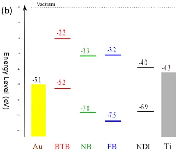
Figure 1. (a) Molecular unit of the oligomers used in this report with their frontier orbitals in
vacuum (HOMO calculated by B3LYP/6-31G* and LUMO deduced from UV-VIS calculation (TD-DFT B3LYP/6-31G(d)) and HOMO level and absorption spectra. (b) Molecular orbital levels in vacuum of the various molecules and Fermi levels of the contact. Oligomer length was set to six aromatic units (phenyl or thiophene) in BTB, NB and FB device while NDI levels are for single NDI molecules since oligo(NDI) are weakly conjugated.68 Note that the frontier orbital energies in vacuum neglect the mutual interaction of the oligomers as well as their interaction with the electrode.
Experimental Methods.
Unless noted otherwise, the MJs were fabricated using a gold stripe substrate on SiO2/Si
wafers with width of 20 µm and several millimeters long. The gold thickness was 45 nm on a Ti adhesion layer (2 nm).After electrochemical deposition of the organic layer, an electron beam Ti/Gold top contact was deposited as described in detail previously.62,63 Each sample allowed the fabrication of 16 molecular junctions with lateral dimensions of 20 by 20 µm (area = 4 x 10⁻⁶ cm2). Careful control of the back pressure during Ti deposition was important, as this very reductive metal can easily be oxidized to various conductive titanium oxides.69-71 A pressure of 10-8 torr was used to reduce oxidation from the residual oxygen and water of the vapor
deposition systems but since reaction of Ti with the organic layer cannot be excluded the molecular/Ti interface was carefully characterized using X-ray photoelectron spectroscopy (XPS). For all junctions using different molecules the Ti/Au top coat deposition was performed with identical conditions and all junctions were also completed using lithography and shadow mask for top electrode deposition. No significant differences were observed using either shadow mask or direct lithography on the molecular layer showing that the fabrication techniques used here are fully compatible with standard microfabrication techniques.
1-(2-bisthienyl)-4- aminobenzene and, N-(4-aminophenyl)-N’-hexylnaphtalene-1,8:4,5-tetracarboxydiimide were synthesized using procedures adapted from literature,66,68,72 this last molecule being synthesized for the first time its characteristics (NMR and High Resolution Mass Spectroscopy) are given in the Supplementary Information (SI files) while tetrafluoroaniline and para amino-nitrobenzene are commercial products and were purchased from Aldrich. Their corresponding diazonium salts were generated in situ using ter-butylnitrite (Aldrich) as a reagent. This procedure has been described in detail.19,66,67,73,74
Organic layer thicknesses were determined by AFM measurements. The thickness of the gold stripe deposited on SiO2 was first measured using AFM profile. The thickness of the gold
stripe covered by the grafted layer was then measured and the thickness of the organic layer was deduced by subtracting the gold thickness75 using a statistical procedure as shown in Figure S1. Standard deviations of thickness were in the range of 0.4 to 0.8 nm as indicated in Table S1. Junction designations include subscripts indicating layer thicknesses in nanometers, with all devices using the same bottom and top contact electrodes. For example, Au45/BTB9/Ti2/Au45
indicates a layer of 9 nm of BTB formed electrochemically on 45 nm or Au followed by 2 nm of Ti and 45 nm of Au top contact deposited in vacuum.
Current density vs bias voltage (JV) electrical characteristics of molecular junctions were measured in air with a Keithley 2602b source-meter at 2 V.s-1 or by dc polarizing the junction while measuring the current with a low-noise current amplifier. In each case a two-probe set-up configuration was used with the top electrode grounded while applying a bias to the bottom electrode. The resulting current-density/voltage (JV) curves exhibited no hysteresis when acquired in air, or in vacuum (<10-5 torr for several hours, Figure S2-a). All JV curves in figures were obtained in air, and each curve presented in figures is a representative curve of JV characterization obtained with the MJs fabricated on each sample.
Low temperature measurements were performed using a variable temperature insert at a base temperature of 5 K while keeping the sample in He atmosphere. The device was allowed to heat from 5 K to room temperature while successive JV curves were recorded.
XPS analysis was performed using Kratos AXIS XPS with Al Kα radiation and depth profiling with a 4 kV Ar+ beam at 5 x 10⁻¹⁰ torr. “Blanket” samples on 1.8 x 1.3 cm silicon surfaces covered with a pyrolyzed photoresist film64. Deposition of the BTB layer (d=9 nm) was achieved using the same procedure as that for molecular junctions, and 2 nm of Ti and 20 nm of Au were deposited at <2 x 10⁻⁷ torr pressure. The thinner Au layer was required by subsequent depth profiling. Survey and high resolution spectra for C, S, O, and Ti were obtained initially and during Ar+ etching at intervals of 120 seconds. CasaXPS software was used for deconvolution of the XPS spectra using a Shirley baseline and Gaussian-Lorentzian line shapes.
Results
The bottom metal/BTB structure shown in Figure 2a has been described in detail previously, and consists of oligothiophene based molecules bonded by covalent bonds to the gold bottom contact.67 Such layers exhibit unique on/off switching of their transport properties in an
electrochemical environment. Insulating behavior is observed below 0.65 V/SCE, whereas BTB films become conductive above this potential. As a consequence, such systems combine the advantages of conductive oligomers with those of diazonium-based layers, i.e. fine control of the film thickness in the 2 to 20 nm range, ability to generate robust, pinhole-free, electroactive layers with two redox states of different conductivity which can be considered switchable organic electrodes.
Current-density vs applied voltage (JV) curves for Au/BTB9/Ti2/Au MJ are shown in
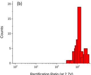
Figure 2a, for the case of ~ 9 nm thick films of BTB (overlay of several JV curves collected on various junctions are given in Figure S3). As reported previously, JV curves for BTB layers between Au and Ti/Au are not symmetric with respect to polarity provided the thickness, d of the molecular layer, is greater than 5 nm. Indeed large currents are observed when the bottom electrode is positively polarized at moderate bias whereas when negatively polarized the current flowing through the junction is much smaller. Figure S4 shows that the rectification ratio (RR) varies with applied potential and reaches a plateau at 2.7 V, and Figure 2b shows histograms of the rectification ratio at +2.7 V (RR2.7V) obtained with 63 different devices produced on different
samples (Of the 64 junctions tested, 63 showed behavior similar to figure 2a, for a yield of 98% when using 9 nm BTB layers). Average RR2.7V is 1200 with few devices showing RR2.7V at 300
and some devices with RR2.7V as high as 3000. Such rectification ratios are, to the best of our
knowledge unprecedented for a single component molecular junction. They are reproducible and devices show long term stability (over a year). No dependence on scan rate from 0.1 to 100 V.s-1 was observed (see Figure S5). Temperature dependent measurements showed that rectification was still observed at 7 K (see figure S2c-d, RR for BTB decreases with decreasing temperature, by a factor of 10 between 300 and 7 K, but is still large at 7 K) and transport was activation-less
in the 7 to 100 K temperature range, with an Arrhenius slope < 5 meV (Figure S2-c) and an activation barrier of 150 meV was measured from 200 to 300 K in agreement with previous results.15 These findings indicate that activation or reorganization before electron transfer are not important for transport and rectification at low temperature and exclude redox events involving Titanium dioxide69,76 as being at the origin of the observed rectification properties.
Since similar BTB layers sandwiched between two carbon electrodes show symmetric JV curves15 we can attribute at first glance the large RR ratios observed here to the use of two different metals with different work functions for contacting the BTB layer.
-3 -2 -1 0 1 2 3 -0.5 0.0 0.5 1.0 1.5 2.0 2.5 Curre nt Dens ity ( A.cm -2 ) Applied Voltage (V) 9 nm BTB
(a)
Figure 2: a) Average Current-density vs applied voltage (JV) curves for Au/BTB9/Ti2/Au MJs
inset Schematic illustration of a molecular junction with a 9 nm thick layer of bis-thienylbenzene (BTB) grafted on a gold electrode followed by the direct deposition of a Ti(2 nm)/Au(45 nm) top electrode.). Note that the number of BTB units involved in the device is more than 2. b) Rectification Ratio (J(+2.7 V)/J(-2.7 V)) histogram for 63 Au/BTB9/Ti2/Au junctions
Ti metal can be easily oxidized to TiO2 during the fabrication process, and has been
already reported to be the origin of rectification in molecular junctions.69,76 To rule out the involvement of TiO2 in the rectification mechanism, we acquired XPS depth profiles during Ar+
etching to yield the elemental composition of Si/SiO2/PPF/BTB9/Ti2/Au20 made identically to the
Au/BTB9/Ti2/Au molecular junctions but on a 1.8 x 1.3 cm area. Figure 3a shows the atomic
percentages (%) -vs- etching time (s) of this structure before and during Ar-ion etching in the XPS chamber. At the beginning of the etching process only Au signal is observed, as expected, but after 360 s of etching the Au signal decreases and simultaneously Carbon and Titanium atomic percentage start to increase. Note that Titanium and Carbon signal increase before oxygen signal which start to be seen at 600 s etching time and the atomic percentage for O1s remains
lower than that of Titanium at all etching depths. Note also that the sulfur signal increases only 100 101 102 103 0 5 10 15 20 Counts
Rectification Ratio (at 2.7V)
(b)
after 700 s and that the C/S ratio reaches the theoretical value of 7 expected for a BTB layer when etching time is between 800 and 960 s. Similar experiments were performed on a Si/SiO2/PPF/Ti2/Au20 large-area sample and are shown in figure S6. In that case Au decreases
and simultaneous Carbon, Titanium and Oxygen signals increase (but no sulfur) are also observed with Titanium atomic % being again always above that of oxygen. This excludes the formation of a 2 nm thick TiO2 layer in the device, and indicates that the Ti layer is mainly TiII
and TiIII oxides, presumably mixed and disordered. Such “sub-oxides” TiO and Ti2O3 contain
mobile conduction band electrons and are considered metallic.69,77-79 There is no evidence that the TiOx layer contains significant TiO2, and it therefore behaves like a metal rather than a large
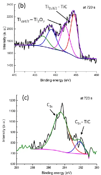
Figure 3: a) Atomic percentages (%) -versus- Etching time (s) for a Si/SiO2/PPF/BTB9/ Ti2/Au20
b) Titanium high resolution XPS signal, c) Carbon high resolution XPS signal.
Figure 3b and c show the high resolution XPS spectra of the Titanium and the Carbon regions at 720 seconds etching time, at which point the oxygen signal is at its maximum. No Ti0 signal at 454.0 eV is apparent in the spectra which implies nearly total reaction of the metallic Ti
during deposition. No signal for the Ti2p3/2 and Ti2p1/2 peaks of TiO2 at 459.0 eV and 464.7 eV are
observed, but two types of Titanium are present. The first one shows Ti2p3/2 and Ti2p1/2 at 455.5
and 460.7 eV and can be assigned to TiC or TiO species with an area of more than 60% of the total high resolution Ti2p signal whereas the second one at 457.1 and 462.5 eV can be attributed to some Ti2O3 species.80-83 The presence of Ti-C bonds is also confirmed by the strong C1s signal
observed at 282.1 eV (see figure 5c) while that of Carbon signal of the BTB moieties are seen at 284.3 eV.
Overall, this detailed XPS analysis clearly indicates that the Ti layer used in the BTB devices is not transformed in TiO2 but that some Titanium atoms bind to the molecules and
create covalent C-Ti bonds at the molecule/top electrode interface. The completed MJ is electrically equivalent to a BTB layer between two metallic electrodes, with at least partial covalent bonding between the molecule and each electrode. The rectification observed in this work cannot thus be explained by redox events involving TiO2.
The dependence of rectification on molecular structure was investigated by first replacing BTB with NB and FB (structures in Figure 1) layers of similar thicknesses. Oligo(NB) is a moiety that is less easily oxidized than oligo(BTB), with a free-molecule HOMO at -7.0 eV while that of BTB is -5.2 eV (see Figure 1). Oligo(FB) is a system with a large HOMO-LUMO gap as it is based on phenylene moieties bearing fluorine substituents. When grafted on gold by diazonium electroreduction fluorinated oligoparaphenylenes are generated. Polyparaphenylene is known to have a band gap of 3 eV84 and the presence of four fluorine groups on each benzene rings in FB will increase the bandgap further by inducing a greater degree of inter-ring torsion between adjacent phenyl units. It is thus likely that the HOMO-LUMO gap of this layer is close
to that of a single AF unit and significantly above that of BTB and NB. DFT Calculations for sexi(FB) oligomer predict a HOMO at -7.5 eV and a HOMO-LUMO gap close to 4.3 eV.
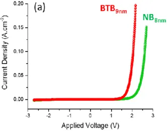
Figure 4a and b compare the J(V) curves of Au/NB8/Ti2/Au (green curve) and of
Au/FB8/Ti2/Au (blue curve) junctions to that of Au/BTB9/Ti2/Au (red curve). The same data are
displayed in lnJ versus V in figure S7. NB and FB devices are consistently much less conductive than BTB devices as the measured current in the -2.7 V, +2.7 V potential range are smaller at all voltages. FB devices are also clearly less conductive than NB devices and the current scale had to be zoomed in figure 4b for comparison with BTB junctions. Moreover, Figure 4a shows that NB devices also rectify with a rectification ratios (J(+2.7 V)/J(-2.7 V) between 50 and 100 that is clearly lower that those observed with BTB devices. On the contrary FB devices show weak rectification behavior (RR between 1 and 3) in the bias range between -2.7 and +2.7 V. These clear variations of the current densities and rectification ratios with molecular structure are a strong indication of a molecular signature relating structure to conductance and electronic behavior when using aromatic films of 8 to 9 nm thicknesses between Au and Ti/Au electrodes.
Figure 4: a) Current-density vs applied voltage (JV) curves for a) Au/NB8/Ti2/Au (green curve)
and Au/BTB9/Ti2/Au (red curve) MJ b) for Au/FB8/Ti2/Au (blue curve) and Au/BTB9/Ti2/Au
(red curve) c) for Au/NDI7/Ti2/Au (gray curve) and Au/BTB9/Ti2/Au (red curve) MJ d)
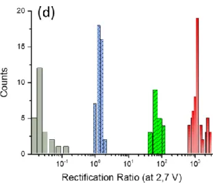
Rectification Ratio (J(+2.7 V)/J(-2.7 V) histograms for 63 BTB (red), 21 NB (green) and 42 FB (blue) devices and 26 NDI (gray) junctions
As BTB layers consists of easily p-dopable oligomers and can be conductive above 0.6 V/SCE in electrochemical environment, we turned to layers based on NDI which is known to be easily reduced in an electrochemical environment (reduction potential at -0.5 and -0.7 V/SCE see figure S8) and is a n-dopable material widely used in organic electronics. This molecule also incorporates a terminal alkyl chain that may change the electronic coupling with the top Ti/Au electrode despite covalent Ti-C bonds. Details on the grafting procedure and the characterization of the Au/NDI modified electrode used here are given in the Figure S8. As shown in Figure 1, the HOMO and LUMO energies for BTB and NDI in vacuum differ significantly, with the low LUMO energy of NDI (-4.0 eV) making it an acceptor with an energy close to the contact Fermi level of Ti or TiC85.
Figure 4c compares the J(V) curve of Au/NDI7/Ti2/Au (gray curve) to that of
devices over the entire -2.7 V, +2.7 V potential range investigated. Importantly, the direction of rectification in the NDI device is reversed compared to that observed in BTB devices with larger J observed when the substrate bias is negative, i.e. when the potential of the Ti/Au layer is more positive than that of the Au/NDI top contact.
Figure 4d shows the rectification ratio (J(+2.7 V)/J(-2.7 V) histograms of more than 150 different devices (63 BTB, 21 NB and 42 FB and 25 NDI) while Figure S7-d overlays the results obtained with the four different molecular layers in lnJ versus V. The electronic behavior of the studied devices clearly depends on the molecular structure of the layers with a high level of confidence statistically. Figure 4d also makes it possible to draw several intermediate conclusions about the effect of molecular structure on JV response in single component layers contacted by Au and Ti/Au. First, single-component layers can support electron transport across molecular layer thicknesses of 9 nm, too thick to be explained by coherent tunneling between the contacts. Second, a large difference in conductance between NDI7, NB8, FB8, and BTB9 (Figure 4
a, b and c) is observed when such differences were not observed for different aromatic structures with thicknesses below 5 nm.19 The weak effect of orbital energies on JV response when d < 5 nm was attributed to strong electronic coupling between the contacts and the aromatic molecules, which causes deviation from classical Mott-Schottky behavior. This coupling induces a “leveling” effect (or “vacuum level shift”) which is known to occur at metal/organic interfaces. 86-88
However, above 5 nm, single-component layers of NDI, NB, FB and BTB current densities differ by orders of magnitude. This result clearly indicates that molecular structure and orbital energies have pronounced effects on JV behavior for aromatic MJs with d > 5 nm and reveals that the “leveling” effect is limited to ~ 5 nm from the conducting surface in aromatic devices. Third, all reported cases of single-component molecular layers between symmetric carbon
contacts yielded nearly symmetric JV response, with RR < 28,15,89 while NDI7 and BTB9 layers
between Au and Ti/Au contact are strongly asymmetric, with RR statistically below 0.01 and above 1000 respectively, i.e. with RR changing by five orders of magnitude. Such variations of RR with molecular structure are significantly larger than those reported in the literature.
Some mechanistic conclusions are provided below, but the experimental evidence clearly indicates that when the organic layer thickness between Au and Ti/Au contacts is large enough to avoid direct tunneling (i.e. d > 5 nm) rectification which depends strongly on molecular structure is possible for low bias voltages. Rectifying MJs can be reproducibly fabricated and their behaviors are robust due to the diazonium grafting process which bonds covalently to the bottom electrode. The rectification behavior clearly originates from the asymmetric contacts but also shows a strong dependence on molecular structure, of both rectification ratio and polarity.
As already stated, rectification must include an asymmetric feature along the transport direction. Contacts based on conductive materials of different work function, bilayers with a donor and an acceptor part in which unidirectional charge transport is favored (Aviram Ratner or reverse Aviram Ratner current flow), redox groups in the layer, or layer contacted by chemisorption to the bottom electrode and physisorption to a top electrode have been reported to be at the origin of rectification in previous work. Since the MJ structure in the present case differs from most of the previous studies, several factors might contribute to the rectification mechanism. However the current results clearly demonstrate that both contacts and molecular structure can affect rectification and we consider several of these factors below.
The offset between the molecular orbitals and the contact Fermi level is often used to estimate the tunneling barriers for MJs and to identify the main charge carrier flowing through the device. The Fermi level of Au90 is 5.1 to 5.2 eV vs vacuum while that of Ti and TiC is at
-4.3 eV85. BTB HOMO is close to the Au Fermi level and is separated from that of Ti or TiC by only ~1 eV while the barrier between BTB LUMO and the Fermi levels of either contact is much higher. This suggests that transport in BTB involves holes and agrees with previous reports based on transport15 and photocurrents.88,91 Moreover, when using BTB layers where covalent bond formation has been experimentally evidenced both at bottom and top electrodes, we propose that the difference in barriers for hole injection associated with strong coupling at both electrodes is important to the origin of the large rectification (RR >1000) behavior observed for BTB based devices.
Figure 5 shows a plausible scheme explaining the rectification of BTB devices. It shows only the oligo(BTB) HOMO levels as BTB acts as a hole transporting layer and p-dopable species in electrochemical experiments.67 Four HOMO levels have been arbitrarily represented as molecular relays for intrachain hopping across the 9 nm thick layer. Note that the exact number of hopping steps remains unknown and that it lies between 2 and 7 as the size of a hole in a oligo(BTB) layer is 4-5 nm and that of one BTB unit is 1.3 nm. 92 We assume strong coupling occurs at the Au/BTB interface due to the presence of Au-C chemical bonds and the BTB HOMO being close to the Au FFermi level, and therefore hole injection at this interface is near resonance with a small barrier. In other words, we can assume that part of the BTB layer acts as an extended electrode with almost no barrier for holes injection at the Au/BTB interface.62 The presence of TiC at the BTB/Ti/Au top interface also leads to strong coupling but the initial barrier for hole injection at this interface is much higher. As a consequence Fermi level pinning is expected at both interfaces and the difference in work function between Au and TiC generates the energetic scheme depicted in figure 5a at zero bias with the four BTB HOMO levels decreasing in energy from the Gold to the Titanium electrode. The barrier between the
BTB HOMO and Ti, noted 1 in Figure 5 is significantly larger than that between BTB and Au.
Since the barrier for hole formation in BTB at the Au/BTB interface is smaller than the barrier at the TiC electrode, we expect holes to form in BTB HOMO levels under positive bias. Once these holes are created it is possible for the TiC electrode to compensate the resulting positive charge by injecting electrons into the emptied HOMOs of the oligomers. Note that transport can be obtained by tunneling from a molecular state in resonance with the Fermi level of the electrode (straight arrows) but also by activated processes depicted in Figure 5b by curved arrows. When the bias is reversed as in Figure 5c, hole injection from the BTB layer into Ti is energetically much less favorable for two reasons. First, the applied biashas to compensate for the initial (1)
barrier located at the BTB/TiC interface. Second, tunneling from a molecular state of an oligoBTB moiety in resonance with an empty level in the electrode will be slower because of a larger tunneling distance. As a consequence, at -2.7 V little current crosses the devices as depicted in figure 5c. As Fermi level pinning occurs at BTB/TiC interface, decreasing 1 is
difficult and needs to reach bias above -2.7 V to allow the coupled HOMO of oligo(BTB) at the BTB/TiC interface to rise close to the Fermi level of titanium, and participate in charge transport. Moreover, a bias above 2.7 V will also be needed to allow a molecular state with small enough tunneling distance to reach resonance with the Fermi level of the titanium electrode.
(a) V = 0V
(b) V = +2.7V
(c) V = -2.7V
f
1f
1Figure 5: Plausible mechanism explaining the large rectification for the Au/BTB/Ti/Au devices i.e. Energy diagram at different applied biases a) zero, b) positive + 2.7 V c) negative -2.7 V. Work functions of 5.1 eV and 4.3 eV are assumed for a polycrystalline Au surface and a Ti surface, respectively. 1 represents the initial barrier between coupled oligo(BTB) HOMO and
Fermi level of TiC whereas that between coupled oligo(BTB) HOMO and Au Fermi level is taken as close to zero for clarity. Note that the exact number of hopping steps remains unknown
This proposed mechanism, involving strong electronic coupling and Fermi level pinning at both interfaces can reasonably rationalise the large rectification observed for BTB. Note that this mechanism explains also easily the temperature dependence of the current observed at positive or negative bias (see Figure S2). Indeed, for positive bias, the thermally activated current observed between 100 and 290 K with low activation energy of 150 meV can be attributed to the small barrier at the Au/BTB interface whereas, for negative bias no observable activation in the same temperature range are observed as a result of the large barrier at the BTB/TiC interface. It also predicts that the RR ratio in BTB devices is mainly linked to the initial barrier and to the Fermi level pinning at the BTB/TiC interface of the top contact. Decreasing this barrier or the Fermi level pinning at this interface, by any means, will decrease the RR observed. Figure S9 shows an extreme case in which electronic coupling is negligible at the top electrode as if the layer were studied using STM with Ti tip. In that case, it is easier to compensate for the initial (1) barrier located at the weakly coupled BTB/Ti interface by
applying negative bias which decreases sharply the rectification ratio. The situation shown in figure 5b is also consistent with a preferential current flow for positive bias with NB, i.e, in the same direction as that observed with BTB (see Figure SIX) and a smaller RR observed for FB. The lower energy HOMOs in the latter case creates significant barriers at both interfaces, thus decreasing J and RR.
It is however not possible using this mechanism to explain the reversal of rectification polarity for NDI-based devices. The NDI LUMO is only 0.3 V above the Fermi level of Ti and TiC while its HOMO is 2 V below that of gold which suggests that transport mainly involves electron injection in NDI MJs with molecular layer thicknesses above the direct tunneling limit between the two electrodes. This is confirmed by photocurrent experiments on NDI junctions which are consistent with LUMO mediation.91This injection will be much easier at the NDI/Ti interface as depicted in Figure 1b so that if electronic coupling is similar at both electrodes, current will be stronger for positive bias, i.e. in the same direction as that observed in BTB devices. This is clearly not observed here as electrons are experimentally more easily injected in the NDI layer at negative bias i.e. when the Au bottom electrode is negative and Ti/Au top electrode is positive. As a consequence, we propose that the direction of the rectification observed with NDI-based devices can be explained if the couplings of the molecular layer with the contacts are not the same as those demonstrated in BTB-based devices, despite the identical conditions used for fabrication of the devices. One plausible explanation is that weak coupling occurs at the bottom Au/NDI interface as a result of a LUMO localized (see Figure S10) on the central part of the NDI molecule and a large energy difference between the NDI LUMO and the Fermi level of Au. It is also possible that NDI is less strongly coupled at the Ti interface compared to BTB due to the long alkyl moiety which is known to induce a decoupling effect.93 Assuming such situation, higher current can be obtained when the device is negatively biased depending on the relative coupling strength at each electrode as recently demonstrated in single molecule junction.94 More complex scenarios can also be considered as molecular resonance between HOMO and LUMO orbitals inside a molecular chain leading to bipolar transport.95 Full explanation of the mechanism behind rectification in NDI-based devices is beyond the scope of
this work and experiments including XPS depth profile and varying the length of the alkyls moieties will be reported elsewhere. Moreover, a full understanding of the rectification mechanism discussed in this study may be achieved by state of the art theoretical modelling that includes the entire system using a non-equilibrium Green’s functions (NEGF) approach 96,97
Conclusions
Molecular junctions with thicknesses between 7 and 9 nm using two contacts of different work function exhibit significant changes in electronic behavior with variation of molecular structure of the layer. Using oligo(bisthienylbenzene) layer, a molecule whose HOMO energy level in vacuum is close to the Fermi level of the gold bottom electrode, the devices exhibit robust and highly reproducible rectification ratios above 1000 at low voltage (2.7 V). Higher current is observed when the bottom gold electrode is biased positively and Ti/Au is negative. When the molecular layer is based on molecule with high HOMO-LUMO gap, i.e. tetrafluororobenzene, no rectification is observed while the direction of rectification is reversed if the molecular layer consists of molecules with low LUMO energy level, i.e. naphthalene diimides and incorporates alkyl moieties. Rectification persisted at very low temperature (7 K), and was activation-less between 7 and 100 K. The results show that rectification is induced by the asymmetric contacts but is also directly affected by orbital energies of the molecular layer. A “molecular signature” relating structure to transport through layers with thicknesses above those used when direct tunneling dominates is thus clearly observed and RR changing by five orders of magnitude is demonstrated in this regime. The rectification mechanism is discussed in terms of electronic coupling between molecules and contacts and can be understood if one considers that such coupling depends on the molecular layer structure, since the same fabrication process has
been used for all studied junctions. These observations clearly demonstrate a rectifying molecular junction can be “designed” by controlling the HOMO and LUMO energies as well as the electronic coupling at the interfaces.
ASSOCIATED CONTENT Supporting Information
Supplementary materials are available free of charge via the Internet at http://pubs.acs.org. Synthesis of NDI compound, electrochemical reduction conditions, determination of molecular layer thickness by AFM, temperature dependence measurement of Au/BTB9nm/Ti2nm/Au device,
Overlaid JV curves of several MJs devices, Rectification ratio versus applied Voltage, Scan rate dependence on Au/BTB9nm/Ti/Au MJs, Atomic percentages Versus Etching time (s) for a
Si/SiO2/PPF/ Ti2/Au20, Ln J vs V curves of BTB, NDI, FB, NB molecule junctions,
electro-activity of NDI modified carbon electrode, energetic diagram and plausible mechanism assuming electronic coupling is negligible at the top electrode, LUMO shape of NDI molecules
Corresponding Authors
ACKNOWLEDGMENT
This work was supported the French Agence Nationale de la Recherche under Grant ANR-15-CE09 0001-01) and by the University of Alberta, the National Research Council of Canada, the National Science and Engineering Research Council and Alberta Innovates.
References
(1) Xiang, D.; Wang, X.; Jia, C.; Lee, T.; Guo, X. Chem. Rev. 2016, 116, 4318-4440. (2) Metzger, R. M. Chem. Rev. 2015, 115, 5056-5115.
(3) McCreery, R. L.; Yan, H.; Bergren, A. J. Phys. Chem. Chem. Phys. 2013, 15, 1065-1081. (4) Vilan, A.; Aswal, D.; Cahen, D. Chem. Rev. 2017, 117, 4248-4286.
(5) Yoon, H. J.; Shapiro, N. D.; Park, K. M.; Thuo, M. M.; Soh, S.; Whitesides, G. M. Angew.
Chem., Int. Ed. 2012, 51, 4658-4661.
(6) Tran, E.; Duati, M.; Mullen, K.; Zharnikov, M.; Whitesides, G. M.; Rampi, M. Adv. Mater. 2006, 18, 1323.
(7) Li, C.; Pobelov, I.; Wandlowski, T.; Bagrets, A.; Arnold, A.; Evers, F. J. Am. Chem. Soc. 2008, 130, 318-326.
(8) Bergren, A. J.; McCreery, R. L.; Stoyanov, S. R.; Gusarov, S.; Kovalenko, A. J. Phys. Chem.
C. 2010, 114, 15806-15815.
(9) He, J.; Chen, F.; Li, J.; Sankey, O. F.; Terazono, Y.; Herrero, C.; Gust, D.; Moore, T. A.; Moore, A. L.; Lindsay, S. M. J. Am. Chem. Soc. 2005, 127, 1384-1385.
(10) Capozzi, B.; Dell, E. J.; Berkelbach, T. C.; Reichman, D. R.; Venkataraman, L.; Campos, L. M. J. Am. Chem. Soc. 2014, 136, 10486-10492.
(11) Choi, S. H.; Kim, B.; Frisbie, C. D. Science 2008, 320, 1482-1486. (12) Luo, L.; Choi, S. H.; Frisbie, C. D. Chem. Mater. 2011, 23, 631-645.
(13) Choi, S. H.; Risko, C.; Delgado, M. C. R.; Kim, B.; Bredas, J.-L.; Frisbie, C. D. J. Am. Chem.
Soc. 2010, 132, 4358-4368.
(14) Hines, T.; Diez-Perez, I.; Hihath, J.; Liu, H.; Wang, Z.-S.; Zhao, J.; Zhou, G.; Müllen, K.; Tao, N. J. Am. Chem. Soc. 2010, 132, 11658-11664.
(15) Yan, H.; Bergren, A. J.; McCreery, R.; Della Rocca, M. L.; Martin, P.; Lafarge, P.; Lacroix, J. C. Proc. Natl. Acad. Sci. U. S. A. 2013, 110, 5326-5330.
(16) Aviram, A.; Ratner, M. Chem. Phys. Lett. 1974, 29, 277-283.
(17) Xie, Z.; Bâldea, I.; Smith, C. E.; Wu, Y.; Frisbie, C. D. ACS Nano 2015, 9, 8022-8036. (18) Kim, B.; Choi, S. H.; Zhu, X. Y.; Frisbie, C. D. J. Am. Chem. Soc. 2011, 133, 19864-19877. (19) Sayed, S. Y.; Fereiro, J. A.; Yan, H.; McCreery, R. L.; Bergren, A. J. Proc. Natl. Acad. Sci. U.
S. A. 2012, 109, 11498-11503.
(20) Mujica, V.; Ratner, M. A.; Nitzan, A. Chem. Phys. 2002, 281, 147-150.
(21) Elbing, M.; Ochs, R.; Koentopp, M.; Fischer, M.; von Hänisch, C.; Weigend, F.; Evers, F.; Weber, H. B.; Mayor, M. Proc. Natl. Acad. Sci. U. S. A. 2005, 102, 8815-8820.
(22) Stadler, R.; Geskin, V.; Cornil, J. J. Phys.: Condens. Matter 2008, 20, 374105.
(23) Berlin, Y. A.; Grozema, F. C.; Siebbeles, L. D. A.; Ratner, M. A. J. Phys. Chem. C 2008, 112, 10988-11000.
(24) Van Dyck, C.; Ratner, M. A. Nano Lett. 2015, 15, 1577-1584.
(25) Metzger, R. M.; Chen, B.; Höpfner, U.; Lakshmikantham, M. V.; Vuillaume, D.; Kawai, T.; Wu, X.; Tachibana, H.; Hughes, T. V.; Sakurai, H.; Baldwin, J. W.; Hosch, C.; Cava, M. P.; Brehmer, L.; Ashwell, G. J. J. Am. Chem. Soc. 1997, 119, 10455-10466.
(26) Vuillaume, D.; Chen, B.; Metzger, R. M. Langmuir 1999, 15, 4011-4017.
(27) Nijhuis, C. A.; Reus, W. F.; Whitesides, G. M. J. Am. Chem. Soc. 2009, 131, 17814-17827. (28) Yuan, L.; Breuer, R.; Jiang, L.; Schmittel, M.; Nijhuis, C. A. Nano Lett. 2015, 15, 5506-5512.
(29) Yuan, L.; Nerngchamnong, N.; Cao, L.; Hamoudi, H.; del Barco, E.; Roemer, M.; Sriramula, R. K.; Thompson, D.; Nijhuis, C. A. Nat. Comm. 2015, 6, 7324.
(30) Chabinyc, M. L.; Chen, X.; Holmlin, R.; Jacobs, H.; Skulason, H.; Frisbie, C. D.; Mujica, V.; Ratner, M.; Rampi, M. A.; Whitesides, G. M. J. Am. Chem. Soc. 2002, 124 11730-11736.
(31) Trasobares, J.; Vuillaume, D.; Théron, D.; Clément, N. Nat. Comm. 2016, 7, 12850. (32) Souto, M.; Yuan, L.; Morales, D. C.; Jiang, L.; Ratera, I.; Nijhuis, C. A.; Veciana, J. J. Am.
(33) Metzger, R. M. Chem. Phys. 2006, 326, 176-187.
(34) Metzger, R. M.; Mattern, D. L. In Unimolecular and Supramolecular Electronics II:
Chemistry and Physics Meet at Metal-Molecule Interfaces; Metzger, R. M., Ed.; Springer Berlin
Heidelberg: 2012, p 39-84.
(35) Lenfant, S.; Krzeminski, C.; Delerue, C.; Allan, G.; Vuillaume, D. Nano Lett. 2003, 3, 741-746.
(36) Meany, J. E.; Johnson, M. S.; Woski, S. A.; Metzger, R. M. ChemPlusChem 2016, 81, 1152-1155.
(37) Johnson, M. S.; Kota, R.; Mattern, D. L.; Metzger, R. M. Langmuir 2016, 32, 6851-6859. (38) Hihath, J.; Bruot, C.; Nakamura, H.; Asai, Y.; Díez-Pérez, I.; Lee, Y.; Yu, L.; Tao, N. ACS
Nano 2011, 5, 8331-8339.
(39) Díez-Pérez, I.; Hihath, J.; Lee, Y.; Yu, L.; Adamska, L.; Kozhushner, M. A.; Oleynik, I. I.; Tao, N. Nat. Chem. 2009, 1, 635-641.
(40) Batra, A.; Darancet, P.; Chen, Q.; Meisner, J. S.; Widawsky, J. R.; Neaton, J. B.; Nuckolls, C.; Venkataraman, L. Nano Lett. 2013, 13, 6233-6237.
(41) Lee, Y.; Carsten, B.; Yu, L. Langmuir 2009, 25, 1495-1499.
(42) Koiry, S. P.; Jha, P.; Aswal, D. K.; Nayak, S. K.; Majumdar, C.; Chattopadhyay, S.; Gupta, S. K.; Yakhmi, J. V. Chem. Phys. Lett. 2010, 485, 137-141.
(43) Nijhuis, C. A.; Reus, W. F.; Siegel, A. C.; Whitesides, G. M. J. Am. Chem. Soc. 2011, 133, 15397-15411.
(44) Nijhuis, C. A.; Reus, W. F.; Whitesides, G. M. J. Am. Chem. Soc. 2010, 132, 18386-18401. (45) Kuikka, M. A.; Li, W.; Kavanagh, K. L.; Yu, H.-Z. J. Phys. Chem. C 2008, 112, 9081-9088. (46) Zhao, J.; Yu, C.; Wang, N.; Liu, H. J. Phys. Chem. C 2010, 114, 4135-4141.
(47) Vezzoli, A.; Brooke, R. J.; Ferri, N.; Higgins, S. J.; Schwarzacher, W.; Nichols, R. J. Nano
Lett. 2017, 17, 1109-1115.
(48) Capozzi, B.; Xia, J.; Adak, O.; Dell, E. J.; Liu, Z.-F.; Taylor, J. C.; Neaton, J. B.; Campos, L. M.; Venkataraman, L. Nat. Nano. 2015, 10, 522-527.
(49) Zhang, W.; Zhang, X.; Lu, C.; Wang, Y.; Deng, Y. J. Phys. Chem. C 2012, 116, 9227-9234. (50) Jin, Y.; Friedman, N.; Sheves, M.; Cahen, D. Langmuir 2008, 24, 5622-5626.
(51) Li, Y.; Calder, S.; Yaffe, O.; Cahen, D.; Haick, H.; Kronik, L.; Zuilhof, H. Langmuir 2012, 28, 9920-9929.
(52) Popoff, R. T. W.; Zavareh, A. A.; Kavanagh, K. L.; Yu, H.-Z. J. Phys. Chem.C 2012, 116, 17040-17047.
(53) Yu, X.; Lovrinčić, R.; Kraynis, O.; Man, G.; Ely, T.; Zohar, A.; Toledano, T.; Cahen, D.; Vilan, A. Small 2014, 10, 5151-5160.
(54) Zhu, L.; Popoff, R. T. W.; Yu, H.-Z. J. Phys. Chem. C 2015, 119, 1826-1831.
(55) Kleemann, H.; Gutierrez, R.; Avdoshenko, S.; Cuniberti, G.; Leo, K.; Lüssem, B. Org.
Electron. 2013, 14, 193-199.
(56) Kleemann, H.; Gutierrez, R.; Lindner, F.; Avdoshenko, S.; Manrique, P. D.; Lüssem, B.; Cuniberti, G.; Leo, K. Nano Lett. 2010, 10, 4929-4934.
(57) Sengoku, T.; Yamao, T.; Hotta, S. J. Non-Cryst. Solids 2012, 358, 2525-2529.
(58) Saracco, E.; Bouthinon, B.; Verilhac, J.-M.; Celle, C.; Chevalier, N.; Mariolle, D.; Dhez, O.; Simonato, J.-P. Adv. Mater. 2013, 25, 6534-6538.
(59) Kong, H.; Sinha, J.; Hoeft, D.; Kirschner, S. B.; Reich, D. H.; Katz, H. E. Org. Electron. 2013,
14, 703-710.
(60) Gong, X.; Tong, M.; Xia, Y.; Cai, W.; Moon, J. S.; Cao, Y.; Yu, G.; Shieh, C.-L.; Nilsson, B.; Heeger, A. J. Science 2009, 325, 1665-1667.
(61) He, S. J.; White, R.; Wang, D. K.; Zhang, J.; Jiang, N.; Lu, Z. H. Org. Electron. 2014, 15, 3370-3374.
(62) Martin, P.; Della Rocca, M. L.; Anthore, A.; Lafarge, P.; Lacroix, J.-C. J. Am. Chem. Soc. 2012, 134, 154-157.
(63) Fluteau, T.; Bessis, C.; Barraud, C.; Della Rocca, M. L.; Martin, P.; Lacroix, J.-C.; Lafarge, P.
J. Appl. Phys. 2014, 116, 114509.
(64) Bayat, A.; Lacroix, J.-C.; McCreery, R. L. J. Am. Chem. Soc. 2016, 138, 12287-12296. (65) Bergren, A. J.; Zeer-Wanklyn, L.; Semple, M.; Pekas, N.; Szeto, B.; McCreery, R. L. J. Phys.:
Condens. Matter 2016, 28, 094011.
(66) Fave, C.; Leroux, Y.; Trippé, G.; Randriamahazaka, H.; Noel, V.; Lacroix, J.-C. J. Am. Chem.
Soc. 2007, 129, 1890-1891.
(67) Fave, C.; Noel, V.; Ghilane, J.; Trippé-Allard, G.; Randriamahazaka, H.; Lacroix, J. C. J.
Phys. Chem. C 2008, 112, 18638-18643.
(68) Kobaisi, M. A.; Bhosale, S. V.; Latham, K.; Raynor, A. M.; Bhosale, S. V. Chem. Rev. 2016,
116, 11685-11796.
(69) Wu, J.; McCreery, R. L. J. Electrochem. Soc. 2009, 156, P29-P37.
(70) Nowak, A. M.; McCreery, R. L. J. Am. Chem. Soc. 2004, 126, 16621-16631.
(71) McCreery, R. L.; Wu, J.; Prasad Kalakodimi, R. Phys. Chem. Chem. Phys. 2006, 8, 2572-2590.
(72) Hayes, R. T.; Wasielewski, M. R.; Gosztola, D. J. Am. Chem. Soc. 2000, 122, 5563-5567. (73) Stockhausen, V.; Trippé-Allard, G.; Van Quynh, N.; Ghilane, J.; Lacroix, J.-C. J. Phys.
Chem. C 2015, 119, 19218-19227.
(74) Stockhausen, V.; Ghilane, J.; Martin, P.; Trippé-Allard, G.; Randriamahazaka, H.; Lacroix, J.-C. J. Am. Chem. Soc. 2009, 131, 14920-14927.
(75) Stockhausen, V.; Nguyen, V. Q.; Martin, P.; Lacroix, J. C. ACS Appl. Mater. Interfaces 2017, 9, 610-617.
(76) Wu, J.; Mobley, K.; McCreery, R. L. J. Chem. Phys. 2007, 126, 024704.
(77) Grigorov, K. G.; Grigorov, G. I.; Drajeva, L.; Bouchier, D.; Sporken, R.; Caudano, R.
Vacuum 1998, 51, 153-155.
(78) Bartholomew, R. F.; Frankl, D. R. Phys. Rev. 1969, 187, 828-833.
(79) Strachan, J. P.; Pickett, M. D.; Yang, J. J.; Aloni, S.; David Kilcoyne, A. L.; Medeiros-Ribeiro, G.; Stanley Williams, R. Adv. Mater. 2010, 22, 3573-3577.
(80) Ottakam Thotiyl, M. M.; Freunberger, S. A.; Peng, Z.; Chen, Y.; Liu, Z.; Bruce, P. G. Nat.
Mater. 2013, 12, 1050-1056.
(81) Restrepo Parra, E.; Arango Arango, P. J.; Benavides Palacio, V. J. DYNA 2010, 77, 64-74. (82) Johansson, L. I.; Hagström, A. L.; Jacobson, B. E.; Hagström, S. B. M. J. Electron.
Spectrosc. Relat. Phenom. 1977, 10, 259-271.
(83) Blackstock, J. J.; Donley, C. L.; Stickle, W. F.; Ohlberg, D. A. A.; Yang, J. J.; Stewart, D. R.; Williams, R. S. J. Am. Chem. Soc. 2008, 130, 4041-4047.
(84) Lacaze, P. C.; Aeiyach, S.; Lacroix, J. C. In Handbook of Organic Conductive Molecules and
Polymers; Nalwa, H. S., Ed.; Wiley: 1997; Vol. 2, p 205-264.
(85) Santerre, F.; El Khakani, M. A.; Chaker, M.; Dodelet, J. P. Appl. Surf. Scien. 1999, 148, 24-33.
(86) Vilan, A.; Yaffe, O.; Biller, A.; Salomon, A.; Kahn, A.; Cahen, D. Adv. Mater. 2010, 22, 140-159.
(87) Braun, S.; Salaneck, W. R.; Fahlman, M. Adv. Mater. 2009, 21, 1450-1472.
(89) Morteza Najarian, A.; Szeto, B.; Tefashe, U. M.; McCreery, R. L. ACS Nano 2016, 10, 8918-8928.
(90) Karipidou, Z.; Branchi, B.; Sarpasan, M.; Knorr, N.; Rodin, V.; Friederich, P.; Neumann, T.; Meded, V.; Rosselli, S.; Nelles, G.; Wenzel, W.; Rampi, M. A.; von Wrochem, F. Adv. Mater. 2016, 28, 3473-3480.
(91) Fereiro, J. A.; Kondratenko, M.; Bergren, A. J.; McCreery, R. L. J. Am. Chem. Soc. 2015,
137, 1296-1304.
(92) Lacroix, J. C.; Chane-Ching, K. I.; Maquère, F.; Maurel, F. J. Am. Chem. Soc. 2006, 128, 7264-7276.
(93) Jia, C.; Migliore, A.; Xin, N.; Huang, S.; Wang, J.; Yang, Q.; Wang, S.; Chen, H.; Wang, D.; Feng, B.; Liu, Z.; Zhang, G.; Qu, D.-H.; Tian, H.; Ratner, M. A.; Xu, H. Q.; Nitzan, A.; Guo, X. Science 2016,
352, 1443-1445.
(94) Sherif, S.; Rubio-Bollinger, G.; Pinilla-Cienfuegos, E.; Coronado, E.; Cuevas, J. C.; Agraït, N. Nanotechnology 2015, 26, 291001.
(95) Tefashe, U. M.; Nguyen, Q. V.; Lafolet, F.; Lacroix, J.-C.; McCreery, R. L. J. Am. Chem. Soc. 2017, 139, 7436–7439.
(96) Zhao J.;Yu, C.; Wang, N.; Liu, H.; Zhao et al., J. Phys. Chem. C 2010, 114, 4135–4141
(97) Liu, W., Cai, S., Deng, X. Journal of Electronic Materials, 2015, 44, 667.
Table of Contents (TOC) artwork
Mis en forme : Anglais