HAL Id: hal-02089153
https://hal.archives-ouvertes.fr/hal-02089153
Submitted on 3 Apr 2019
HAL is a multi-disciplinary open access
archive for the deposit and dissemination of sci-entific research documents, whether they are pub-lished or not. The documents may come from
L’archive ouverte pluridisciplinaire HAL, est destinée au dépôt et à la diffusion de documents scientifiques de niveau recherche, publiés ou non, émanant des établissements d’enseignement et de
Room-temperature InAs/InP Quantum Dots laser
operation based on heterogeneous “2.5 D” Photonic
Crystal
B. Ben Bakir, C Seassal, X. Letartre, Philippe Regreny, Michel Gendry, P.
Viktorovitch, M Zussy, L Cioccio, J Fedeli
To cite this version:
B. Ben Bakir, C Seassal, X. Letartre, Philippe Regreny, Michel Gendry, et al.. Room-temperature InAs/InP Quantum Dots laser operation based on heterogeneous “2.5 D” Photonic Crystal. Optics Express, Optical Society of America - OSA Publishing, 2006, 11, pp.395 - 407. �hal-02089153�
Room-temperature InAs/InP Quantum Dots
laser operation based on heterogeneous
“2.5 D” Photonic Crystal
B. Ben Bakir, Ch. Seassal, X. Letartre, Ph. Regreny, M. Gendry, and P. Viktorovitch
LEOM-CNRS-Ecole Centrale de Lyon
36 Avenue Guy de Collongue, 69134 Ecully Cedex, France
badhise.benbakir@ec-lyon.fr, christian.seassal@ec-lyon.fr
M. Zussy, L. Di Cioccio, and J. M. Fedeli
CEA-DRT / LETI
17, rue des Martyrs, 38054 Grenoble, France
jean-marc.fedeli@cea.fr
Abstract: The authors report on the design, fabrication and operation of heterogeneous and compact “2.5 D” Photonic Crystal microlaser with a single plane of InAs quantum dots as gain medium. The high quality factor photonic structures are tailored for vertical emission. The devices consist of a top two-dimensional InP Photonic Crystal Slab, a SiO2 bonding layer, and
a bottom high index contrast Si/SiO2 Bragg mirror deposited on a Si wafer.
Despite the fact that no more than about 5% of the quantum dots distribution effectively contribute to the modal gain, room-temperature lasing operation, around 1.5µm, was achieved by photopumping. A low effective threshold, on the order of 350µW, and a spontaneous emission factor, over 0.13, could be deduced from experiments.
©2006 Optical Society of America
OCIS codes: (140.5960) Semiconductor lasers; (250.5230) Photoluminescence; (230.3990)
Microstructure devices;(230.5750) Resonators; (230.4170) Multilayers
References and Links
1. Ch. Seassal, C. Monat, J. Mouette, E. Touraille, B. Ben Bakir, H.T. Hattori, J.L. Leclercq, X. Letartre, P. Rojo-Romeo, and P. Viktorovitch, “InP Bonded Membrane Photonics Components and Circuits: Toward 2.5 Dimensional Micro-Nano-Photonics,” IEEE J. Sel. Top. Quantum Electron. 11, 395-407 (2005).
2. P. Caroff, C. Paranthoen, C. Platz, O. Dehaese, H. Folliot, N. Bertru, C. Labbé, R. Piron, E. Homeyer, A. Le Corre, and S. Loualiche, “High-gain and low-threshold InAs quantum-dot lasers on InP,” Appl. Phys. Lett.
87, 243107 (2005).
3. H. Saito, K. Nishi, A. Kamei, and S. Sugou, “Low Chirp Observed in Directly Modulated Quantum Dot Lasers,” IEEE photonic Technol. Lett. 12, 1298-1300 (2000).
4. J. Hendrickson, B. C. Richards, J. Sweet, S. Mosor, C. Christenson, D. Lam, G. Khitrova, H. M. Gibbs, T. Yoshie, A. Scherer, O. B. Shchekin, and D. G. Deppe, “Quantum dot photonic-crystal-slab nanocavities: Quality factors and lasing,” Phys. Rev. B. 72, 193303 (2005).
5. Y. Akahane, T. Asano, B. S. Song, and S. Noda, “High-Q photonic nanocavity in a two-dimensional photonic crystal,” Nature 425, 944-947 (2003).
6. M. Nomura, S. Iwamoto, K. Watanabe, N. Kumagai, Y. Nakata, S. Ishida, and Y. Arakawa, “Room temperature continuous-wave lasing in photonic crystal nanocavity,” Opt. Express 14, 6308-6315 (2006). 7. T. Yoshie, O.B. Shchekin, H. Chen, D.G. Deppe, and A. Scherer, “Quantum dot photonic crystal laser,”
Electron. Lett. 38, 967-968 (2002).
8. B. Ben Bakir, Ch. Seassal, X. Letartre, P. Viktorovitch, M. Zussy, L. Di Cioccio, and J. M. Fedeli, “Surface-emitting microlaser combining two-dimensional photonic crystal membrane and vertical Bragg mirror,” Appl. Phys. Lett. 88, 081113 (2006).
9. M. Gendry, C. Monat, J. Brault, P. Regreny, G. Hollinger, B. Salem, G. Guillot, T. Benyattou, C. Bru-chevallier, G. Bremond, and O. Marty, “From large to low height dispersion for self-organized InAs quantum sticks emitting at 1.55mm on InP (001),” J. Appl. Phys. 95, 4761-4766 (2004).
10. G. Björk, A. Karlsson, and Y. Yamamoto, “Definition of a laser threshold,” Phys. Rev. A 50, 1675-1680 (1994).
11. T. Baba, “Photonic Crystals and Microdisk Cavities Based on GaInAsP–InP System,” IEEE J. Sel. Top. Quantum Electron. 3, 808-830 (1997).
12. Y. Yamamoto, S. Machida, G. Björk, “A Microcavity laser with enhanced spontaneous emission,” Phys. Rev. A 44, 657-668 (1991).
13. T. Baba and D. Sano, “Low-Threshold Lasing and Purcell Effect in Microdisk Lasers at Room Temperature,” IEEE J. Sel. Top. Quantum Electron. 9, 1340-1346 (2003).
14. L. A. Coldren, S. W. Corzine, Diode Lasers and Photonic Integrated Circuits, New York: Wiley (1995) 15. P. Pottier, C. Seassal, X. Letartre, JL Leclercq, P. Viktorovitch; D. Cassagne, C. Jouanin, “Triangular and
hexagonal high Q-factor 2-D photonic bandgap cavities on III-V suspended membranes,” J. Lightwave Technol. 17, 2058-2062 (1999).
16. F. Raineri, C. Cojocaru, R. Raj, P. Monnier, A. Levenson, C. Seassal, X. Letartre, and P. Viktorovitch, “Tuning of a two-dimensional photonic crystal resonance via optical carrier injection,” Opt. Lett. 30, 64-66 (2005).
17. M. Fujuta, R. Ushigome, and T. Baba, “Large Spontaneous Emission Factor of 0.1 in Microdisk Injection Laser,” IEEE photonic Technol. Lett. 13, 403-405 (2001).
18. H. Y. Ryu, N. Notomi, E. Kuramoti, and T. Segawa, “Large spontaneous emission factor (>0.1) in the photonic crystal monopole laser,” Appl. Phys. Lett. 84, 1067-1069 (2004).
1. Introduction
Microlasers are among the key devices for the future on-chip optical links that could be used for optical interconnects or datacom [1]. Such light sources should exhibit not only low power consumption and low footprint, but also an ability to operate at high temperature (due to CMOS circuit heating) and at high modulation rate. Compared to the classical quantum well based lasers, their quantum dot (QD) counterpart potentially offers high temperature stability [2] and a low chirp [3]. Moreover, QDs laser should demonstrate a reduced threshold and a high differential gain, if their size dispersion is sufficiently low.
Additionally, Photonic Crystals (PCs) appear to be the most promising candidates for the design and production of small volume and high quality factor (Q-factor) optical micro-resonators, with a well controlled radiation emission pattern.
Recently, J. Hendrickson et al. have demonstrated low-temperature lasing operation around 1.2µm using a single InAs/GaAs QDs plane and a high Q-factor PC-micro-cavity [4]. Based on the high Q-factor planar microcavity design developed by Y. Akahane et al. [5], they could achieve a threshold power on the order of 200µW. Using a stacked InAs/GaAs quantum dot layers, room temperature (RT) lasing in photonic crystal microcavities was demonstrated around 1.3µm [6-7].
We recently introduced the concept of “2.5D” PC lasers combining 2D PC-Slab and Bragg reflectors, for the control of both optical losses and emission pattern [8]. On the other hand, InAs/InP QD nanostructures have proven to be quite well suited to efficient light emission in the 1.3-1.55µm wavelength range [9]. In this article, we propose to combine such a gain material with a high Q-factor “2.5D” PC resonator, and we investigate the possibility to reach RT laser operation of a single plane of InAs/InP QDs.
2. Design
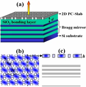
As depicted in Fig. 1(a), we designed a high index contrast “2.5 D” PC constituted of a top 2D PC patterned in a 250nm-thick InP membrane, a SiO2 bonding layer, a Bragg mirror formed
by three pairs of Si/SiO2 quarter-wavelength layers on a Si substrate. The principle of
operation of the device is fully discussed in reference [8]. Basically, the 2D PC-Slab, which is a graphite lattice of air holes, is targeted for vertical operation, i.e., we exploit a resonant band-edge mode located in the center of the first Brillouin zone. Near this point, where the group velocity is very low, the electromagnetic field is laterally confined and is weakly coupled to the radiated continuum. In order to achieve further control over the photon lifetime in such a resonator, we add a reflective vertical structure (Bragg mirror) below the 2D PC-Slab. This perturbative approach can lead to a strong modification of the dynamic behaviour
of the resonant mode. Using this concept, the Q-factor can be maximized with an optimum bonding layer optical thickness of 3λ/4.
Fig. 1. (a) Generic configuration of the simulated devices. (b) In-plane and (c) cross-sectional view of the electromagnetic energy density pattern calculated using 3D plane wave expansion method. The lattice-constant, the radius and the thickness of the PC membrane are: a=775nm, r=130nm, h=250nm. The thickness of the Si and SiO2 λ/4 layers are 110nm and 255nm, respectively.
Additionally, as depicted in Fig. 1(b) and Fig. 1(c), the electromagnetic energy density of the photonic mode is strongly localized in the semiconductor region of the 2D PC-Slab, ensuring a very efficient light-matter interaction.
3. Device fabrication and optical characterization
On the one hand, the III-V heterostructure used for the devices is grown by solid source molecular beam epitaxy. A 300nm-thick sacrificial/etch-stop layer of In0.53Ga0.47As is grown
on a 2-inch InP(001) wafer. Then, a 250nm InP layer is grown, including at mid-height a single plane of InAs QDs. The QDs are elongated in the [1-10] direction so that they present a dash-like shape [9]. On the other hand, the Si/SiO2 Bragg mirror is deposited on a Si wafer by
low pressure chemical vapor deposition. Then, the III-V heterostructure is transferred on top of the Bragg reflector, using SiO2–SiO2 wafer bonding [1]. The InP substrate and etch-stop
layer are eliminated by selective wet chemical etching, leading to the final vertical structure presented in Fig. 2(a) and Fig. 2(b). A 90nm-thick SiO2 layer is then deposited on top of the
structure using plasma-assisted sputtering. Finally, PCs are patterned in a 150nm-thick PMMA mask using electron beam lithography and transferred into silica and InP layers by means of reactive ion etching (Fig. 2(c)). The final devices have a lateral extension of 30µm x 30µm.
The devices are photopumped using a pulsed laser diode emitting at 780nm. The pulse width is 6ns, with a 1.2% duty cycle. The pump beam is focussed under normal incidence with a x20 achromatic objective lens (0.4 numerical aperture), onto an area of about 4µm in diameter. Emission spectra are measured using a high resolution spectrometer and an InGaAs photodetector array.
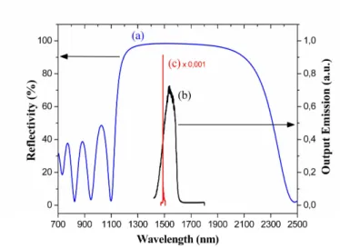
Figure 3 presents the measured Bragg mirror reflectivity (Fig. 3(a)) which is higher than 98% in a broad spectral range (1400–1650nm), and the unpatterned heterostructure emission spectrum (Fig. 3(b)), compared to the typical emission spectrum corresponding to the laser peak of the resonant mode (Fig. 3(c)).
Fig. 2. Scanning electron micrograph: (a) cross-sectional view of the unpatterned heterostructure and (c) top view of the graphite lattice PC membrane. Transmission electron micrograph: (b) cross-sectional view of the InAs quantum dots.
Fig. 3. (a) Reflectivity of the Bragg mirror, and (b) unpatterned heterostructure emission spectrum compared to (c) the typical emission spectrum corresponding to the laser peak of the resonant mode.
4. Results and discussion
Figure 4(a) shows the output emission intensity of the main resonant mode against the incident peak power, Pi (L-L curve) for a first structure. On this figure, we also display the
ratio λ/δλ as a function of Pi, where δλ is the spectral linewidth (Q-L curve). This ratio will be
further referred to as the “experimental Q-factor”. Output emission spectra are also shown in the insets. These spectra show multimode emission for various pumping rate. The main mode,
located at 1495nm, is more intense than the others, and exhibits a low linewidth, but the corresponding peak does not dominate the emission spectrum. This resonant mode lies in the region of the QDs distribution where the gain is reasonably high. The L-L curve exhibits a sub-linear increase of the output intensity. The Q-L curve shows a strong increase of λ/δλ, and then a saturation, for a pumping power over 6mW. For this structure, there is no evidence of laser emission, and the linewidth clamping can be attributed to the saturation of the absorption in the gain medium. The obtained λ/δλ value can then give an estimate of the optical Q-factor of the resonator, which should be around 4200.
A radically different behavior can be observed for specific structures where the detuning between the resonant mode and the optical gain is similar, and provided that the quality of the photonic crystal is higher. In particular, Figure 4(b) shows the L-L and Q-L curves obtained on a second structure, where the resonant mode stands at 1490nm. The spontaneous emission background is also plotted on the L-L curve in Fig. 4(b). One could first note that this background saturates for a pumping power over 250µW, with a very low emitted power. If we now consider the peak at 1490nm, two main regimes can be observed. In a first regime, under 1mW, there is a sub-linear increase of the experimental Q-factor together with a roughly linear increase of the emitted power. The linewidth decrease may be attributed to the saturation of the absorption of the QDs, and laser emission cannot be asserted for the corresponding pumping power range. In the second regime, above 1mW we observe a linear increase on both the L-L and Q-L curves. In particular, the experimental Q-factor is linearly increased until the maximum resolution of the spectrometer is reached (Q≈9000, as indicated in Fig. 4(b)). As a consequence, the spectral linewidth is inversely proportional to the number of photons in the resonant mode. Therefore, and on the basis of classical laser analysis, we can conclude that laser emission occurs in this second regime. One could note that very similar trends were observed on Q-L curves in very recent papers, on laser structures combining photonic crystal cavities and a single layer of QDs at low temperature [4], or photonic crystal cavities and a multi-layer of QDs at room temperature [6].
Finally, we obtained a laser power threshold of about 1mW, but if we take into account that, according to our simulations, only 35% of the optical pump power is absorbed by the InP barriers, this leads to an effective threshold of Peff ≈350µW. Moreover, because of the size
dispersion in the self-organized QDs distribution, the gain spectrum of a large collection of QDs is inhomogeneously broadened. Consequently, not all the QDs contribute to the lasing action, resulting in a relatively high threshold. In our devices, we estimate that only 5% of the QDs are spectrally coupled to the resonant mode. By improving the epitaxial growth processes, in order to reduce size dispersion, we expect, with such devices, a strongly reduced effective laser threshold.
In the case of the second structure, an important property is that the L-L curve shown in Fig.4(b) does not exhibit a strong kink around the lasing threshold. Indeed, the kink is softer than in the case of large lasers, and even of most PC lasers. As shown by different groups, the L-L curve shape is strongly related to the spontaneous emission factor β and the non-radiative recombination rate [10,11]. We stress that, in our case, the non-radiative recombinations on the etched sidewalls are limited due to the lateral confinement of the carriers in the QDs. We recall that the β-factor is defined as the ratio between the spontaneous emission rate into the lasing mode and the total spontaneous emission rate. It can be estimated by this simple relation (see [11-14] for extra details):
4 2 3 mode 4 r l InP QD n V λ β π λ Γ ≅ Δ (1)
Fig. 4. (a) Emission characteristics obtained on structure 1 and (b) structure 2. Output emission power intensity, spontaneous emission (SE) background and measured Q-factors against the incident pump power. The bold dashed-line indicates the maximum resolution of the spectrometer. The dashed circles emphasize the change of behavior around the threshold. Output emission spectra obtained for various pumping powers are displayed in the insets.
where Γr is the relative confinement factor, nInPis the refractive index of the patterned InP layer, Vmode is the volume of the resonant mode, λl the resonant wavelength of the lasing
mode and ΔλQD is the spectral homogeneous broadening at room temperature of the QDs
participating to the lasing action. It is always difficult to evaluate experimentally the mode volume of a band-edge microlaser. Indeed, the technological imperfections tend to reduce drastically the lateral extension of the resonant mode compared to the patterned membrane area. We estimated, by infrared near field imaging, the mode volume, Vmode =1.2 10-11cm-3.
Assuming an averaged relative confinement factor,Γ =r 2, and an homogeneous broadening of individual QD, ΔλQD =5nm, we found β >0.13. In equation (1), the enhancement of spontaneous emission in the lasing mode is taken into account but it is assumed that the total spontaneous emission rate (in all optical modes) remains equal to the value of a QD in a bulk semiconductor. However, as described in [15], in our specific vertical configuration, the direct vertical light emission is significantly inhibited. Then, the calculated value of β is certainly underestimated. Finally, even with a mode volume higher than usual PC microcavities, this estimate shows that the β-factor is relatively large. Considering both this factor and the reduced non-radiative recombination, we are typically in the case where the L-L curve presents a smooth evolution around the threshold.
Figure 5 presents the wavelength shift plotted against the incident pump power (λ-L curve). We first notice that no red-shift can be observed, since the thermal effect is very limited on this sample, owing to the pumping conditions (short pulses and low duty cycle) and because the InP based heterostructure is bonded onto SiO2. The wavelength shift is therefore
mainly attributed to carrier-induced refractive index shift [16]. More precisely, the λ-L curve exhibits a first regime, well under 1mW, where the blue-shift rate is relatively important. For such peak powers, injected carriers tend to reduce the absorption in QDs, and change the modal effective index accordingly. Around 1mW and above, the blue-shift rate is much lower. Similarly to what have been observed and discussed by Fujita et al. [17], and more recently by Ryu et al. in the case of photonic crystal lasers [18], the change from the first to the second regime is gentle, which is accounted for by large β-factors. Moreover, one can note that the wavelength is not clamped at the highest pumping powers. Indeed, in this second regime, although the carrier density tends to saturate in the QDs, the residual blue-shift could be caused by increase of the carrier density in the InP barriers, which subsequently affects the refractive index.
5. Conclusion
We fabricated an original heterogeneous and compact “2.5D” Photonic Crystal microlaser including a single-plane of InAs quantum dots as light emitter. The high Q-factor and directive photonic structure is based on the combination of a 2D PC-Slab with a 1D high index contrast Bragg reflector. An effective threshold of ~350µW could be achieved despite the fact that no more than about 5% of the quantum dot distribution effectively contribute to the modal gain. This is not a record in term of laser threshold, however, according to the best of our knowledge, it is the first time that lasing action at RT is achieved via the association of a Photonic Crystal resonator and a single plane of QDs as gain medium.
We also discussed the influence of the high spontaneous emission factor on the L-L curve characteristics and on the blue-shift of the lasing wavelength above the threshold. We estimated this factor to be higher than 0.13.
Combining our original approach for the design of the micro-resonator with improved QDs growth conditions should result in the production of ultra-low threshold micro-lasers. Acknowledgments
This work was supported by the French National Nanoscience “NALIM” Project and by the ePIX-net European Network of Excellence. We would like to thank Michel Garrigues for fruitful discussions and Olivier Marty for TEM characterization of the QDs.