Digital Assistance Design for Analog Systems:
Digital Baseband for Outphasing Power Amplifiers
by
Yan Li
B.Eng., Electrical Engineering, University of Science and Technology of China (2004) M.A.Sc., Electrical Engineering, McMaster University (2006)
Submitted to the
Department of Electrical Engineering and Computer Science
in partial fulfillment of the requirements for the degree of
Doctor of Philosophy in Electrical Engineering and Computer Science
at the
MASSACHUSETTS INSTITUTE OF TECHNOLOGY
June 2013
@
Massachusetts Institute of Technology 2013. All rights reserved.
A u th or ...
.... ...
Department of Electrical Engineering and Computer Science
A?
March 7, 2013
Certified by...
....
/.
. ...
Associate Professor of Electrical Engineering and Computer Science
Thesis Supervisor
Accepted by...
j1
(bllie A. Kolodziejski
Chair, Department Committee on Graduate Students
,AASSACHUSMTS IN68I1YIE OF TECHNOLOGY
JUL 0 8 20131
LIBRARIES
Digital Assistance Design for Analog Systems: Digital
Baseband for Outphasing Power Amplifiers
by
Yan Li
Submitted to the Department of Electrical Engineering and Computer Science on March 7, 2013, in partial fulfillment of the
requirements for the degree of
Doctor of Philosophy in Electrical Engineering and Computer Science
Abstract
Digital assistance is among many aspects that can be leveraged to help analog/mixed-signal designers keep up with the technology scaling. It usually takes the form of predistorter or compensator in an analog/mixed-signal system and helps compensate the nonidealities in the system. Digital assistance takes advantage of the process scaling with faster speed and a higher level of integration. When a digital system is co-optimized with system modeling techniques, digital assistance usually becomes a key enabling block for the high performance of the overall system. This thesis presents the design of digital assistances through the digital baseband design for outphasing power amplifiers. In the digital baseband design, this thesis conveys two major points: the importance of the use of the reduced-complexity system modeling techniques, and the communications between hardware design and system modeling. These points greatly help the success in the design of the energy-efficient baseband.
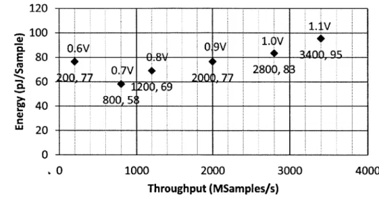
The first part of the baseband design is to realize the nonlinear signal processing unit required by the modulation scheme. Conventional approaches of implementing this functionality do not scale well to meet the throughput, area and energy-efficiency targets. We propose a novel fixed-point piece-wise linear approximation technique for the nonlinear function computations involved in the signal processing unit. The new technique allows us to achieve an energy and area-efficient design with a throughput of 3.4Gsamples/s. Compared to the projected previous designs, our design shows 2x improvement in energy-efficiency and 25x in area-efficiency.
The second part of the baseband design devotes to the nonlinear compensator design, aiming to improve the linearity performance of the outphasing power amplifier. We first explore the feasibility of a working compensator by use of an off-line iterative solving scheme. With the confirmation that a compensator does exist, we analyze the structure of the nonlinear baseband-equivalent PA system and create a dynamical real-time compensator model. The resulting compensator provides the overall PA system with around 10dB improvement in ACPR and up to 2.5% in EVM.
Thesis Supervisor: Vladimir M. Stojanovid
Acknowledgments
I am fortunate enough to spend more than six years at MIT, enjoying the accom-pany of great people while striving to reach the end of my PhD journey. I have to give my first 'thank you' to my advisor Professor Vladimir Stojanovid. There is a common word in Chinese describing a good teacher: teach by precept and example, and Vladimir perfectly interprets it with his self-example. As a supervisor, he plans, teaches, and guides each individual in the group; as a researcher, he works with great passion and energy, inspiring me to explore the fields that I have never thought of. I am very thankful for the opportunity to work with him for the past years and I am sure the knowledge and qualities I learnt from him will benefit me throughout my career path.
I would like to thank my thesis committee: Professors Alexander Megretski and Joel Dawson, for their patience with my thesis, as well as the research advise in various projects. I have been in collaboration with them closely in research projects for quite a long time, especially with Alex. Being a mathematician, Alex is always keen on the root of the problem and extremely helpful in providing insights to many problems.
I would like to thank Yehuda for his effort in weaving the net of people where everyone is able to find his/her comfort place and works as a team seamlessly. His talk with me from time to time always brings wisdom which probably would take me a long time to find by myself.
I would like to thank Mar Hershenson and her old team of Sabio for the opportu-nity to work with them as an intern. I am fortunate to be able to enjoy the spirit of entrepreneurship as well as the sunshine in California.
I would like to thank all past and current ISG folks. I am grateful for having them around throughout the tape-outs, various dry runs. Without the effort they put into our ISG's infrastructure, it would be a different story with all my tape-outs. I want to give my special thanks to my three officemates: Natasha, Michael and Jonathan. They are the best officemates you can ask for.
I would like to thank all my friends and family, who share my happiness and bitterness in my life. You are the ones I can always trust and get support from, and I am grateful to have you in my life. Lei became my husband the year I entered MIT. We worked in adjacent buildings, sometimes attended the same class, and when I stayed up for tape-outs or paper, he always prepared everything for me. I am thankful to have his encouragement, support, and the positive attitude throughout the journey, and I am sure he is as happy as I am for my graduation. Finally, I would like to thank my parents, Lixian and Anqi. No better words for you than 'I love you, dad and mom'.
Contents
1 Introduction
1.1 Challenges in the Analog World . . . . 1.2 Digitally Fix the Analog World . . . . 1.3 Thesis Contributions . . . . 1.3.1 Nonlinear Signal Processing for the Digital Baseband of AMO
P A . . . .
1.3.2 Reduced-complexity System Modeling and PA Compensator D esign . . . . 1.3.3 Extension of System Modeling to Hierarchical System Opti-m ization . . . . 1.4 Thesis Overview . . . . 2 Nonlinear Signal Processing in a Digital Baseband Design of RF
Transmitter
2.1 Outphasing Power Amplifier Background 2.1.1 LINC and AMO Systems . . . . 2.2 Piece-wise Linear Approximation . . . . . 2.2.1 Algorithm . . . . 2.2.2 Piece-wise-linear Design Example . 2.2.3 Comparison with General Numerical 2.3 Chip Implementation . . . . 2.3.1 Overall Design . . . . 2.3.2 Blocks Design . . . . Function 19 19 20 21 22 23 25 25 27 28 28 30 30 38 40 41 41 44 Generation
2.3.3 Experimental Results . . . . 50
2.4 Sum m ary .. .... .... ... . .. ... . . . . 56
3 Reduced-complexity System Modeling in Compensator Design for an RF Transmitter 57 3.1 Digital Predistortion for PA System ... 58
3.1.1 Overview of Popular Digital Predistortion Techniques . . . . . 58
3.1.2 Linearity M etrics . . . . 59
3.2 Digital nonlinear compensation for the LINC and AMO Systems . . . 60
3.2.1 System Setup . . . . 60
3.2.2 Iteration-based Off-line Predistortion for LINC/AMO Systems 65 3.2.3 Analysis of Nonlinearities Throughout the System . . . . 79
3.2.4 Real-time Predistortion Model for LINC/AMO Systems . . . . 85
3.2.5 Implementations . . . . 93
3.3 Limitations of the Models . . . . 98
3.4 Sum m ary . . . . 105
4 A Hierarchical System Design Methodology 107 4.1 Proposed Hierarchical Design Methodology . . . . 107
4.2 Design Space Reduction . . . . 108
4.2.1 Equation-based Circuit Optimization . . . . 109
4.2.2 Equation-based Robust Circuit Optimization . . . . 111
4.3 Subsystem Abstraction . . . . 113
4.4 Sum m ary . . . . 119
5 Conclusions and Future Research Directions 121 A Zero-avoidance Filter Design Example Using Heuristics 125 B Robust Iterative Optimization Algorithm for Analog Circuits 129 B.1 Algorithm . . . . 129
B.1.2 Sources of Variability . . . . 130 B.2 Experimental results . . . . 139 B.2.1 A two-stage op-amp example . . . . 139
List of Figures
2-1 (a) LINC, AMO SCS. (b) AMO PA system overview. ... 29
2-2 (a) The general concept of PWL approximation. (b) Proposed fixed-point PWL approximation. . . . . 32
2-3 (a) Micro-architecture of the PWL approximation. (b) Illustration of the computations in the PWL approximation. . . . . 35
2-4 The block diagram of the chip . . . . 41
2-5 The hardware block diagram of the SCS system. . . . . 42
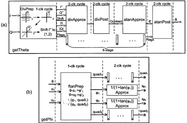
2-6 (a) The hardware block diagram of the get Theta block. (b) The hard-ware block diagram of the getPhi block. . . . . 45
2-7 The hardware block diagram of the getAlpha block. . . . . 48
2-8 Spectrum and EVM of the SCS. . . . . 51
2-9 Throughput and energy with supply scaling for AMO SCS. . . . . 52
2-10 Chip photograph. . . . . 53
2-11 (a) Power breakdown of the AMO SCS design. (b) Area breakdown of the AMO SCS design. . . . . 54
3-1 Three common nonlinear dynamical system structures. (a) Wiener model. (b) Hammerstein model. (c) Wiener-Hammerstein model. . . 58
3-2 An illustration of the ACPR definition. . . . . 60
3-3 PA system under compensation. . . . . 61
3-4 LINC and AMO PA architecture block diagrams. . . . . 62
3-5 Simplified schematics of the cascode class-E PA. . . . . 62
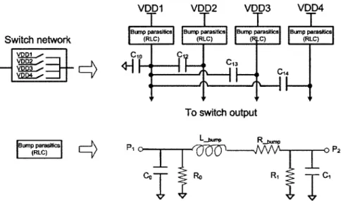
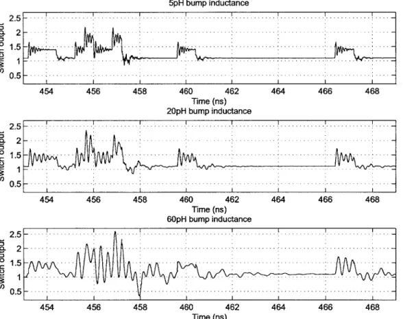
3-7 Switch network output for different values of bump inductances. 4 VDD levels are 1.1V, 1.4V, 1.8V, 2.2V. Sample duration is 0.4ns. . . 64 3-8 PA system under compensation. . . . . 66 3-9 Frobenius norm of the Jacobian of the function v -+ v1. a = 1. . . . . 68
3-10 Frobenius norm of the Jacobian of the function G1(v). a1, a2 C [1.1, 1.4, 1.8, 2.2]. The corresponding threshold levels for different regions
are [2.2, 2.5, 2.8, 3.2, 3.6, 4, 4.4] . . . . 69
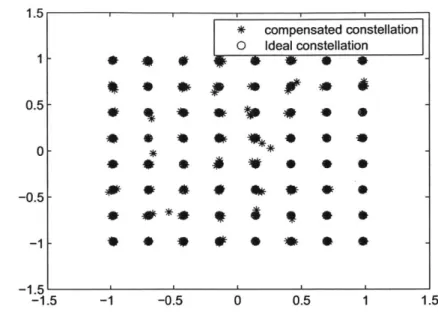
3-11 EVM of the uncompensated LINC system. . . . . 74 3-12 EVM of the compensated LINC system, with real-time zero-avoidance
input sequence. ... ... 75 3-13 Input and output ACPR of the LINC system, with real-time
zero-avoidance input sequence. . . . . 75 3-14 EVM of the uncompensated AMO system with Lbump=20pH. . . . . . 78 3-15 EVM of the compensated AMO system with Lbump=20pH. Input
se-quence is generated from offline level-avoidance filter. . . . . 78 3-16 Input and output ACPR of the AMO system with Lbup=20pH. Input
sequence is generated from offline level-avoidance filter. . . . . 79 3-17 Nonlinear system of the overall transceiver signal chain. . . . . 80 3-18 Illustration of the derivation for nonzero terms in equation (3.31). . 82
3-19 An example of DFT Pi(e3-')) with ri/T = 0.2, 2/T = 0.3, r = 10. 85
3-20 Placement of the compensator in the LINC/AMO systems. . . . . 86 3-21 Compensator structure . . . . 87 3-22 EVM of the LINC system with real-time compensator. Input sequence
is generated from a real-time zero-avoidance filter. . . . . 88 3-23 ACPR of the LINC system with real-time compensator. Input sequence
is generated from a real-time zero-avoidance filter. . . . . 89 3-24 EVM of the AMO system without a real-time compensator. . . . . . 90 3-25 EVM of the AMO system with a real-time compensator. The input
3-26 ACPR of the AMO system with a real-time compensator. The input sequence is generated from an offline level-avoidance filter. . . . . 92 3-27 Construction of the LTI system with discontinuities at +r. . . . . 95 3-28 The block diagram of the compensator hardware implementation. . . 96
3-29 The block diagram of the digital baseband with AMO SCS and
non-linear compensator. . . . . 99 3-30 Overview of the integrated transmitter system with digital baseband
nonlinear compensation. . . . . 100 3-31 The area breakdown of the digital baseband with nonlinear compensator. 100 3-32 The power breakdown of the digital baseband with nonlinear
compen-sator. This is an estimation from post-layout analysis at 1GHz clock frequency. . . . . 101 3-33 Input sequence structure to test the nonlinear system's stability. . . . 101 3-34 An example of constructing output comparisons with fixed previous 4
and the current samples. . . . . 102 3-35 An example of output waveform differences with the same previous
state and current input phases. The state includes four previous samples. 102 3-36 The 12 norm error of all data sets with the same previous state and
current input phase. Different curves represent the states containing different number of past samples. . . . . 103 3-37 The 12 norm error of all data sets with the same previous state and
current input phase for the body-tied PA design. Different curves rep-resent the states containing different number of past samples . . . . . 104 4-1 Hierarchical system design. . . . . 108 4-2 The two-stage Op-amp schematic. . . . . 109 4-3 Design trade-off sets between gain and load capacitance, corresponding
to grid 1 . . . . 110
4-5 The folded-cascode example with Gm E [0.5 mS, 0.6 mS] from opti-mization: Monte-Carlo check with the initial and final robust design. 114 4-6 Monte-Carlo check with the initial and final robust designs: Gm of the
folded-cascode op-amp. . . . . 115 4-7 Parameter grid. Red dots are the designs used to generate
parameter-ized m odel. . . . . 117 4-8 Parameterized system identification results . . . . 117 4-9 Testing results. The x-axis represents 30 testing input patterns and for
each x value, there are 121 y values, denoted as colored '+', to represent the maximal relative error of the model output compared with the spice output in time domain. The '*' represent the maximal difference of the outputs from spice among the 121 designs for a certain input pattern (some x value). The 30 input patterns have random frequencies in the ranges [DC 146MHz] for the patterns 1-10, [DC 1MHz] for the patterns 11-15, [1MHz 10MHz] for the patterns 16-20, [10MHz 50MHz] for the patterns 21-25, [50MHz 146MHz] for the patterns 26-30. . . . . 118 4-10 A coarser parameter grid 2. . . . . 119 4-11 Testing results of the doubled-range parameter model. The x-axis
rep-resents 30 testing input patterns and for each x value, there are 121 y values, denoted as colored '+', to represent the maximal relative error of the model output compared with the spice output in time domain. The '*' represent the maximal difference of the outputs from spice among the 121 designs for a certain input pattern (some x value). The 30 input patterns have random frequencies in the ranges [DC 146MHz] for the patterns 1-10, [DC 1MHz] for the patterns 11-15, [1MHz 10MHz] for the patterns 16-20, [10MHz 50MHz] for the patterns 21-25, [50MHz 146MHz] for the patterns 26-30. . . . . 120 A-1 Illustration of the zero-avoidance zone. . . . . 126 A-2 Illustration of the zero-avoidance filter design. . . . . 126
A-3 Result of a zero-avoidance filter design. . . . .1
B-i Flow of the iterative robust algorithm. . . . . 130
B-2 The two-stage Op-amp schematic. . . . . 131
B-3 Transistor Macro model. . . . . 133
B-4 Monotonicity of circuit performances on variation variables in a two-stage op-amp example. . . . . 134
B-5 Monotonicity of circuit performances along random lines in variation variable space in a two-stage op-amp example. . . . . 135
B-6 Constraint maximization with two variation variables. . . . . 137
B-7 Two-stage op-amp with 1-corner initial optimization design: yield im-provement of gain and we, power and area consumptions. . . . . 140
B-8 Two-stage op-amp five-corner optimization design: yield improvement on gain, w, and power, area consumptions. . . . . 141
B-9 Two-stage op-amp five-corner optimization design: DC gain and w' comparison of initial and final robust designs. . . . . 143
List of Tables
2.1 LINC and AMO SCS Equations . ... ... 28
2.2 Storage comparison examples between a direct LUT map approach and fixed-point piece-wise linear approximation approach. . . . . 36 2.3 Comparison between PWL, CORDIC implementations of the 16-bit
input, output function y(x) = cos'(x). . . . . 36 2.4 Criterion for power supply pair selection. (A2 = J2 +
Q
2) . . . . 43 2.5 Summary of arithmetic operations in each functional block of the AMO
SC S. . . . . 44
2.6 Summary of accuracy and LUT size of the PWL approximated function blocks. . . . . 48 2.7 Comparison with other works. . . . . 55 3.1 ACPR and EVM performances of LINC system in off-line iterations,
with input sequence generated from a real-time zero-avoidance filter. 74 3.2 ACPR and EVM performance comparisons between using input
se-quence with and without zero-avoidance property for LINC systems. The zero-avoidance filter has a real-time implementation as shown in
Appendix A . . . . 76
3.3 Comparison of offline iteration results with real-time and offline zero-avoidance filters. . . . . 77 3.4 ACPR and EVM performances of AMO systems with different bump
inductances. The input sequences are from offline level-avoidance fil-tering. . . . . 77
3.5 ACPR and EVM performances of AMO system with 5pH bump induc-tance and 15ps path mismatch between phase and amplitude paths. The input sequence is generated from offline level-avoidance filter. . 79 4.1 The folded-cascode op-amp example: specifications for nominal design 113 4.2 Folded-cascode op-amp: iterations of the robust designs from
optimiza-tion: gm E [0.5 mS, 0.6 mS]. k denotes the range of the variability. Please refer to Section B. . . . . 113 B.1 Specifications for nominal design . . . . 132 B.2 Robust two-stage op-amp designs in iterations from optimization and
Hspice simulation . . . . 140 B.3 Five-corner of the two-stage op-amp initial design. . . . . 141
Chapter 1
Introduction
1.1
Challenges in the Analog World
A combination of process scaling and demands for performance scaling brings ever-increasing challenges to analog/mixed-signal system designs. As the technology scal-ing front keeps pushscal-ing to the 22nm and 14nm nodes [1], designers are faced with more severe and new varieties of device non-idealities. While miniaturization in size and downward scaling of supply voltage benefit the digital world with faster transistors, a higher level of integration of digital functions and lower power consumption, devices in the scaled analog world suffer from decreased transistor intrinsic gain, dynamic range and larger process variations.
On the other hand, more functionality, lower power and cost, faster speed and ease of use have been driving generations of new products. One of the most prominent examples is the cellular handset, which evolved from a simple portable phone to a personal device capable of operating in multi-band, equipped with Wi-Fi connectivity, high-resolution camera etc. Furthermore, the bars of low-power and area are not lowered considering the integration of all kinds of functionalities. Battery life in portable devices has never been satisfying and researchers from all different disciplines are focusing on more energy-efficient and area-efficient designs.
Despite all the difficulties analog circuits are facing from process and performance scaling, the need for analog/mixed-signal can never be eliminated. Interfaces between
the human, environment and digital processing always exist and the requirements on convenience, flexibility, robustness etc. become even more challenging. To tackle all these problems and keep up with scaling, innovations have to come from all dif-ferent aspects of the chip design. New device process, analog architecture, system architecture, etc. have to all come together and work in an interdisciplinary way.
1.2
Digitally Fix the Analog World
One part of the interdisciplinary effort to improve the analog/mixed-signal system design is through the digital assistance. As the driving force of process scaling, digital design has enjoyed the benefits of faster speed, more integration and lower power consumption. These benefits bring more computational power to the digital system, which can be utilized to correct non-idealities in the analog systems.
Digital assistance usually takes the form of a digital predistortor or compensator. For power amplifier (PA) systems, digital predistortion has been a popular way to enhance the linearity of the system without sacrificing power efficiency by power back-off [2-4]. A digital compensator has also been used in several other communication subsystems, such as modulators [5,6] and analog-to-digital converters (ADCs) [7,8]. Among all these successful examples, we observe two critical factors determining the feasibility of the digital compensation: theoretical support in system design and implementation practicality. Theoretical support from digital signal processing and nonlinear system modeling lays the foundation of the digital compensator design, while the equally important implementation part determines the actual hardware architecture. To achieve the success in the two factors, it is important to bridge the two sides and optimize the algorithm and hardware efficiency simultaneously. In this thesis, the main theme is to demonstrate the effectiveness of the co-optimization of both algorithm and hardware in the context of the digital baseband design for the outphasing power amplifiers.
1.3
Thesis Contributions
There are two main contributions in this thesis: 1) the design and implementation of an energy and area-efficient signal component separator (SCS) for the multi-level asymmetric outphasing (AMO) power amplifier (PA), and 2) reduced-complexity sys-tem modeling and compensator implementation for outphasing PAs. In addition, as an extension of the application of system modeling techniques, we demonstrate several key enabling techniques for a hierarchical system optimization methodology.
The two main parts of the thesis are dedicated to the design of the digital base-band of the outphasing PA. This effort contributes to the new generations of high-throughput wireless communication systems at millimeter-wave (mm-wave) range [9-15]. The availability of large chunks of bandwidth and maturity of CMOS process technology provide the opportunity to address several large markets with bandwidth-demanding communication applications. These mm-wave applications place great challenges on the transceiver design due to factors such as PA efficiency and lin-earity, high loss in wireless channel and multipath, increasing parasitics for passive components, limited amplifier gain etc. Even in cellular base stations, the drive to-ward flexible, multi-standard radio chips, increases the need for precision, high-throughput and energy-efficient backend processing. The desire to best leverage the available spectrum for these high-throughput applications creates the demand for high-efficiency and high-linearity PAs. While these conflicting PA design requirements have been satisfied in the past at low system throughputs by designing smart dig-ital back-ends, the multi-GSamples/s throughput required in new applications puts a significant challenge on digital baseband system design to perform the necessary modulation and predistortion operations at negligible power overhead.
This desire for a high-throughput energy-efficient digital baseband becomes es-pecially prominent for the outphasing PAs designed to improve the efficiency while satisfying the high-linearity requirements for higher-order signal constellations. This is due to the complexity of the baseband digital signal processing which hinders its capability to operate efficiently in high-throughput wideband applications. In this
thesis, we present a solution to extend the applicability of the outphasing PAs to a larger range of wideband applications.
1.3.1
Nonlinear Signal Processing for the Digital Baseband
of AMO PA
The complex digital signal processing task in the baseband for the outphasing PA, and especially AMO PA, is the signal component separator (SCS). The SCS decomposes an arbitrary two-dimensional vector to two vectors under certain constraints. At low throughputs (10-10OMSamples/s), the outphasing PAs would rely on complex digital signal processing to generate the outphasing vectors and make it possible to use simple, high-efficiency switching PAs on each path. At high (multi-GSamples/s) throughputs, however, a radical redesign of the signal component separator (SCS) digital signal processing implementations is needed to prevent degradation in net power efficiency due to a significant increase of digital baseband power consumption. The conventional SCS has been traditionally implemented both in analog and digital designs [16-18]. The analog versions of SCS are obviously not suitable for high-speed and high-precision applications, so we only consider the digital SCS im-plementations. The SCS decomposes the original sample signal into two signals as required by the LINC/AMO, and the decomposition involves the computations of sev-eral nonlinear functions. For digitally implemented SCS, a look-up-table (LUT) is the most common way to realize the nonlinear functions. Considering that the past signal separators mainly work below 1OOMSamples/s with low to medium precision, LUT is indeed the simplest and most energy-efficient approach. Even for the recent AMO ar-chitecture, LUT is still a preferable choice for operations under 1OOMSamples/s [19].
However, the traditional LUT-based function map quickly becomes infeasible when the throughput and precision requirements go up to multi-GSamples/s and more than 10-bit range. The LUT size becomes prohibitively large for on-chip implementations with penalties in both area and speed. Besides, the number of LUTs used in the AMO SCS is significantly larger than in the LINC SCS, so the LUT solutions that
can barely work for LINC render AMO implementations infeasible. On the other hand, at these high throughputs a direct nonlinear function synthesis through itera-tive algorithms such as CORDIC [20] or nonlinear filters [21] proves to be more area compact but with prohibitive power footprint for the overall power efficiency of the
PA.
In this thesis, we present the function synthesis algorithms and a corresponding chip implementation, designed using an alternative approach to compute the nonlinear functions: it is both more area and energy-efficient than state-of-the-art methods like LUTs, CORDIC or nonlinear filters. The chip results demonstrate an AMO SCS working at 3.4GSamples/s with 12- bit accuracy and over 2x energy savings and 25x area savings compared to traditional AMO SCS implementation. The new approach is based on the piece-wise linear (PWL) approximation of a nonlinear function. The approximation consists of the computations of LUT, add, and multiply. In order to minimize the computational cost while maintaining high accuracy and throughput, we propose a novel algorithm to find the fixed-point representation of the approximation. The idea of the fixed-point version of the approximation is to use as few operations as possible and minimize the number of input bits to all the operations so as to achieve high throughput. With these considerations, we are able to achieve a fixed-point representation of typical LINC or AMO nonlinear functions, which consists of one small LUT, one adder and one multiplier. The hardware architecture derived from this special algorithm achieves a nice balance between area, energy-efficiency, throughput and computational accuracy.
1.3.2
Reduced-complexity System Modeling and PA
Com-pensator Design
For a transmitter system in compliance with communication standards, linearity metrics in terms of error-vector-magnitude (EVM) and adjacent-channel-power-ratio
(ACPR) have to be met. In order to achieve high linearity in the PA system, the input signal has to back-off from the peak power level to minimize the distortion
associated with that operation region. The situation becomes even worse for wide-band signals that have a high peak-to-average-power-ratio (PAPR), such as widewide-band code-division multiple access (WCDMA) in the universal mobile telecommunications system (UMTS), or orthogonal frequency-division modulation (OFDM) in current 4G LTE standards. Various linearization techniques, such as feedback, analog predistor-tion, and feed-forward, have been adopted to enhance the PA linearity [22-30]. Digital predistortion (DPD) is another promising technique. Compared with other lineariza-tion techniques, it is free of stability issues and has the potential for significantly smaller area and faster speed. However, it does require an adequate modeling effort to achieve an efficient, reduced-complexity dynamical model of the inverse system.
In this thesis, we present a thorough analysis of the PA baseband-equivalent sys-tem as well as it inverse syssys-tem. First, to establish performance bounds, we treat the problem of searching for the inverse system as a general nonlinear system-solving and employ an iterative scheme. The results from the application of the iterative scheme on the LINC/AMO PAs show nearly 15dB of possible improvement in ACPR and up to 1% of EVM. Considering that most previous treatments dealt with the bandwidth of several MHz to hundreds of MHz, and our testbench in simulation works with 2.5Gsamples/s at 45GHz carrier, this constitutes a significant improvement in linear-ity metrics within such wide bandwidth. With the confirmation from the successful iteration that a working compensator does exist, we move next to find the reduced-complexity inverse system model. Through the analysis of the signal-propagation through the nonlinear system, we develop an approximate model structure of the inverse system. The structure includes the concatenation of a nonlinear system with short memory and a special type of LTI system whose discrete Fourier transform has discontinuities at t7r. The model proves its effectiveness with fitted parameters from a simulation testbench, yielding nearly 10dB improvement in ACPR and up to 2% of EVM. Finally, we build an integrated transmitter system with the digital baseband capable of SCS functionality, as well as real-time compensation, for a transmit chain with a phase modulator, a 16-way PA and its power supply switching network. The digital baseband test results are shown in this thesis, and the overall system test
process is still an ongoing work.
1.3.3
Extension of System Modeling to Hierarchical System
Optimization
As an extension of the reduced-complexity modeling discussed in the previous section, we incorporate it into a hierarchical system optimization methodology. This system design methodology aims to help the system designers to allocate resources and spec-ifications optimally for each block and sub-block of the system. This is achieved by decreasing the dimensions of the design space through the Pareto surface generation for each block, as well as the creation of the parameterized model of each block. In the thesis, we demonstrate the two enabling techniques: Pareto surface generation and the parameterized system modeling on the operational amplifier examples.
1.4
Thesis Overview
The thesis is organized as follows. Chapter 2 is devoted to the SCS design for the AMO digital baseband. It introduces the proposed piece-wise-linear algorithm to realize the nonlinear function computations. With this algorithm, we show the system and block architectures fulfilling the SCS computation in the chip design. The chip was tested and demonstrated state-of-the-art performances in energy and area-efficiency.
Chapter 3 presents the compensator design for the AMO/LINC PAs. We first demonstrate the successful off-line iteration scheme to solve for the compensated sequence for any particular input sample sequence. Next, we analyze the nonlinear system and find out the equivalent nonlinear system dynamical model structure which is used to fit the inverse model of the PA nonlinear baseband-equivalent system. We show the effectiveness of the model by applying the input sequence first to the compensator and use its output at the PA input, with the output of the PA showing improvements of 10dB in ACPR and up to 2% of EVM. Furthermore, the limitation of the modeling is investigated. Importantly, floating-body effect in the SOI process
is found the main cause for the compensation performance limits in both dynamical model and off-line iteration as verified through the comparison design for body-tied
AMO PA design.
Chapter 4 discusses the hierarchical system optimization methodology and shows its dependence on the system modeling techniques. We use the proposed equation-based robust optimization method to generate the Pareto surface and employ the modeling techniques to create the parameterized dynamical model for each block. Realization of the two critical points enables an optimized system across different levels.
Chapter 2
Nonlinear Signal Processing in a
Digital Baseband Design of RF
Transmitter
The trend towards high-throughput and portability, driven mostly by the consumer market, is currently pressing the RF transmitter to have ever increasing efficiency and linearity. Even in cellular base stations, the drive toward flexible, multi-standard radio chips increases the need for high-precision, high-throughput and energy-efficient backend processing. In this chapter, we use an outphasing PA system as an example to demonstrate an energy-efficient high-throughput digital baseband design. With an improved linearity and power efficiency trade-off, outphasing PA places more chal-lenges on its digital baseband with a complex nonlinear signal processing block. When combined with a target PA application in wideband millimeter-wave regime, the de-sign becomes even more challenging due to the requirements from high precision, high throughput and stringent power budget. The algorithm we will show in this chapter is able to provide a solution to satisfy the requirements from all different aspects. We see that the algorithmic design success is due to our ability to take full advantage of the energy-efficient and area-efficient hardware blocks in the design process.
2.1
Outphasing Power Amplifier Background
Fundamentally, the idea of the outphasing PA is to decompose the transmitted signal from the Cartesian domain to two signals with polar modulation or its variations. By use of a more efficient and nonlinear switching-mode PA with phase modulation, the overall system's efficiency can be enhanced without sacrificing linearity. There are several popular outphasing architectures, such as linear-amplification-by-nonlinear-component (LINC) proposed by Cox [31], multi-level LINC (ML-LINC) [32], and asymmetric-multilevel-outphasing (AMO) [33-35]. In the following sections, we will use the AMO architecture as our example. However, the algorithm developed for function synthesis in the AMO can be readily applied to broader set of PA designs and RF applications.
2.1.1
LINC and AMO Systems
Both LINC and AMO PAs are outphasing PA architectures and their digital base-bands perform similar computations. The LINC PA architecture is proposed with the motivation to relieve the ever existing trade-off between the power efficiency and linearity performances of the PA. By decomposing the transmitted signal to two constant-amplitude signals, high-efficiency PAs can be used to amplify the two decom-posed signals without sacrificing the linearity. The AMO PA architecture, prodecom-posed in [33-35] improves the average power efficiency further by allowing the two PAs to switch among a discrete set of power supplies rather than fixing a single supply level.
Table 2.1: LINC and AMO SCS Equations.
LINC Equations AMO Equations
A = 12+ Q2
,9
= arctan(-) (linc1) A = T 2+Q 2, 0 = arctan( ) (amol) a, = arcs &+:a = arccos(A) (linc2) i2 a= )
2 arecos( a 2Aa ) (amo2)
_____ ____ ____ _____ ____ 05\ 2Aa2,
P1 = 0 + a, (2 = 0 - a (linc3) P1 = 0 + ai, 02 = 0 - a 2 (amo3)
Q
2
AO S
LINC SCS
(a)
AMO SCS
Multi-level
power supply
PA1 PA2
P Autput
Phase modulato Phase modulator
a
1f(91)
1/(1+tan(<p))
f(p
2)
2Digital baseband (AMO SCS)
t
I, Q symbols
(b)
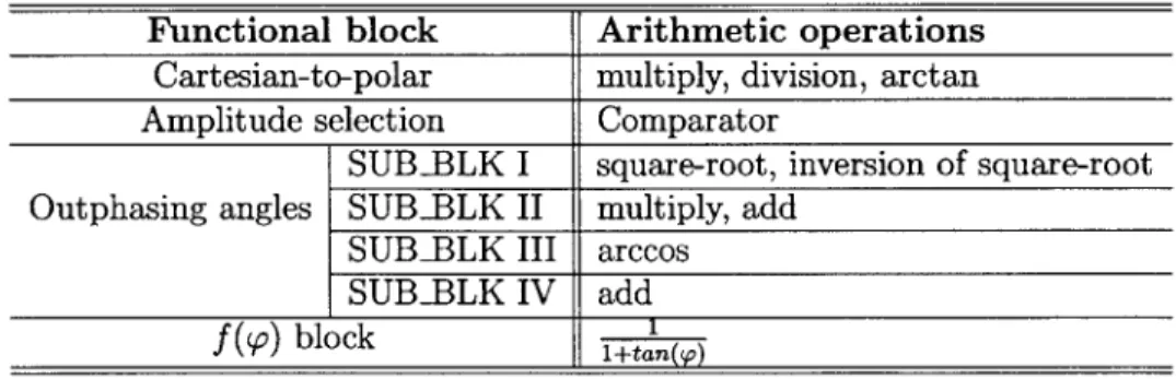
Fig. 2-1(a) shows the working schemes of LINC SCS and AMO SCS for an arbi-trary IQ sample (I,Q). The SCS decomposes the (I,Q) to two signals with phases of S01, 92 and amplitudes of ai, a2, where for LINC ai = a2 = a. The outphasing angles
'p1 and 02 for both architectures are derived from the equations summarized in Table 2.1. In AMO equations, ai, a2 denote the power supplies of the two PAs respectively.
a1, a2 are restricted to the set of V = {V1, V2, V3, V4}, where V V2 V3 V4
are the four levels of supply voltages. Equations in (amo4) of Table 2.1 are in the signal decomposition process simply due to the architecture requirement from the digital-to-RF-phase-converter (DRFPC) [36], which converts the digital outputs to RF modulated signals and takes a function of the phase
f(p)
as the input. Generally, computations in (amo4) depend on the type of the modulator and may be different than what we present here.The typical low-throughput LINC SCS and recent AMO implementations [16-19, 37] usually involve the use of coordinate rotational digital computer (CORDIC) [20] and LUT map for the nonlinear functions in Table 2.1 [18,38. The maturity of the CORDIC algorithm and simplicity of the LUT approach make themselves suitable for the LINC SCS applications whose throughput is below 1OOMSamples/s and with
low to medium resolution ( 8 bits for example). However, the approaches become less attractive or even prohibitive for our target mm-wave wideband applications where the throughput is in the multi-GSamples/s range with high phase resolution (> 10 bits for example). In the next section, we show our proposed solution: using fixed-point PWL approximations on the nonlinear functions which provides a balance
among accuracy, power and area.
2.2
Piece-wise Linear Approximation
2.2.1
Algorithm
The motivation for a new approach to the nonlinear function computation is to replace complex computations with simple and energy-efficient computations. For example,
table look-up with LUTs of reasonable sizes, adders and multipliers are the favorable computations to perform. We also realize that all functions involved in the SCS computations are smooth in almost the whole input range. Hence, they are suitable to be approximated by functions with simple structured basis functions, such as polynomials, splines and etc. These considerations lead us to the PWL function approximation of the nonlinear functions.
Fig. 2-2(a) shows the general application of the PWL approximation to any smooth nonlinear function. The input x is divided into several intervals, where a linear function yj = ai x x + ci, x E [xi, Xi+1) is constructed in each interval to approximate
the actual function value in that range. With this approximation, the computation of the nonlinear function only consists of the linear function computation in each interval (add and multiply), plus a relatively small LUT for the linear function parameters aj, c, in each interval. In terms of accuracy, for any function which has a continuous second-order derivative, the approximation error is bounded by the interval length, the second-order derivative and does not depend on higher-order derivatives, as shown
in [39],
1
lerror
< -(xi+1 - xi)2max
ly"(x)|.
(2.1)8 Xisosomi+
Here, xi, xz+ 1 are the boundaries of the ith interval and y" is the second-order
deriva-tive in x. We observe that the approximation error can be made arbitrarily small as we increase the number of approximation intervals. These initial examinations of the computational complexity and approximation accuracy of the piece-wise linear approximation make it an appealing alternative technique for the LINC and AMO SCS designs.
In order to benefit from the nice properties of the PWL approximation, we need to tailor it to be hardware-implementation friendly. Most importantly, all the arith-metic computations have to be converted to their fixed-point counterparts, and the question is whether the resulting fixed-point computations are able to operate at multi-GSamples/s throughputs with high accuracy. The most seemingly obvious so-lution is a direct quantization of the parameters in the floating-point representation
r
y=f(x)
-' 0 4 'I i +1 Xi+2 Xi+3 '4y
1=aix +c;
(a)
'I
^y=f(x)
D If w ow1 _j
I.ixol
x/00...0
0*01I-x
--
x/1
1...1
x=[xi x21y= k
(x
2-S)
+
bi
(b)
Figure 2-2: (a) The general concept of PWL approximation. (b) Proposed fixed-point PWL approximation.
of the approximation formula. However, this may not be an optimal solution if throughput is the major concern and bottleneck, because the operands of the add and multiply ai, ci are quantized to have the same long bits as the output, and these long-bit arithmetics are likely to be in the critical timing path. Further optimization of the long multiplication would only add complexity to the design. In what follows, we present a modified formulation of the fixed-point PWL approximation and show its capability of running at a much higher throughput than the direct quantization version of the approximation.
The setup of our problem is to compute a nonlinear function of m-bit output with m-bit input x E [0, 1), using the PWL approximation. An m-bit input x can be decomposed to x1 and x2 as x =
[
xi , x2], where m
= m1+m 2. Naturally,mi-MSB bit m2-LSB bit
x1 divides the input range to 2" intervals and it is the indexing number of those
intervals. Fig. 2-2(b) shows an enlargement of the ith interval of the approximation, where x1 takes its ith value, and X2 takes 2 12 values, ranging from 0 to 2Tl2 -1. Under
this setup, we have our proposed fixed-point scheme shown in (2.2).
y2= b
-1
+ki(x2 - Si -1), i=0,1, ...2
m-
1. (2.2)mi-MSB bit m2-LSB bit
Here, yi = [y([i, 0]), y([i, 1]),--
,
y([i, N2 - 1])]T, x2 = k[0, 1, -.,
N2 - 1]T, 1 = [1, 1, -,1
E RN2, Ni = 2m, N2 = 2 2, N = 2', m = m1 + M2, ki, Si, bi C R andthey are all fixed-point numbers.
The underlying idea of this formulation is to compute the m-bit output part by part. In the linear function of each interval, we use the term bi to represent the most significant mi bits of the function value, and the term k2 - (X2 - Si -1) to achieve the lower-significant m2 bits of accuracy. Then y. is simply the concatenation of the two
parts. The procedures to find the fixed-point representations of the three parameters
ki, Si, bi in (2.2) are described in the following steps.
Step 1: Obtain the floating-point version of the PWL approximation. The optimal real coefficients of the linear function in each interval in terms of the 12
norm can be found by least-square optimization (2.3), where the design variables are kr and bi7 E R. The superscripts denote that they are floating-point real numbers; x2
and yi are defined as in (2.2).
mi
| yi - (k -.x 2+br
-1) ||2, for i = 0, 1,2, ..., N1-
1, (2.3)The approximation error bound in (2.1) shows that the error is proportional to (xi+1
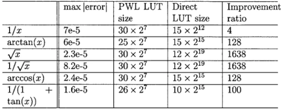
-x,)2, which in the fixed-point input case, equals 2-2mi. Let mi = rm/2-1, then it is possible to realize the required output m-bit accuracy with only 2'm/2' intervals. Since the number of intervals determines the number of address bits of the LUT that stores the parameters of the linear function in each interval, this LUT (2' m/2' entries)
is considerably smaller than a direct map from input to output (2' entries). The following steps determine the fixed-point parameter values, i.e., the content of the
LUT.
Step 2: Obtain the fixed-point value bi.
bi can be achieved simply by quantizing the b to mi-bit. As we mentioned before, the m-bit output is constructed part by part with b as the constant term in the ith interval, representing the major part of the function value in that interval. As long as the functional value increment in each interval is less than 2-m, that is, the functional derivative
ly'(x)l
< 1, it is enough to use the mi-MSB of bi to represent the mi-MSB of the output.Step 3: Obtain the fixed-point value Si.
Since Step 2 yields a bi with a maximum quantization error of 2-m1, to compensate
for the accuracy loss of br - bi, an extra parameter Si is introduced such that kiST =
br - bi. Its fixed-point counterpart Si is derived as in (2.4)
Si = quantize((br - bi)/(kf)). (2.4)
The number of bits of Si is determined such that krS; has the accuracy of m +1 bits. From our experience with the functions involved in the SCS design, Si usually has the number of bits around or a few more (i.e. 2-4) bits than m/2, depending on the
derivative ki of the function in each interval. Step 4: Obtain the fixed-point value ki.
The slope of the function in the ith interval k; can also be obtained by simply quan-tizing its floating-point counterpart from the optimization procedure in Step 1. As shown in (2.2), the term k2(x2 - Si -1) contributes to the second part of the output
- the m2 LSBs. Since x2 - Si has an accuracy of at least m bits, k has to have at
least m2 bits to make the m2 LSBs of the output.
(a)
"
X2-SSi
(X2-Si) L~(X
2-Si)KConcatenation
bi
HE!Midibi+(X2-Si)K
(b)
Figure 2-3: (a) Micro-architecture of the PWL approximation. (b) Illustration of the computations in the PWL approximation.
The above procedure not only provides a way to obtain the three fixed-point parameters of the linear function in each interval, but also provides benefit in the high-throughput hardware architecture design. Fig. 2-3(a) shows the micro-architecture of the approximation and (b) shows more clearly how the computations are carried out. There are essentially 3 arithmetic operations involved: LUT, one adder, and one multiplier. The LUT takes the mi MSBs of the input as the address
and outputs the parameters bi, ki, Si in the corresponding interval. Then the linear function computations follow accordingly. From Fig. 2-3(a), we notice that for all arithmetic computations, the operands have only mi, m2 or i + m2 bits, but not m
bits as input. As we discussed in Step 1, it is a good choice to set mi = 'Im/2-1, hence with operands of m/2 bits (roughly) in all computations, we are able to achieve the m-bit output.
Table 2.2: Storage comparison examples between a direct LUT fixed-point piece-wise linear approximation approach.
map approach and
m Direct LUT size Li (bits) Approx. LUT size L2 (bits) Improvement ra-tio(L1/L2)
10
10x2
10 20x2 5 2412 12x212 24x26 25
14 14x214 28x2 7 26
16 16x216 32x28 27
Table 2.3: Comparison between PWL, CORDIC implementations of the 16-bit input, output function y(x) = cos-'().
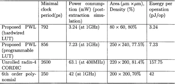
Minimal Power consump- Area (pm x pm), Energy per clock tion (mW) (post- Density
(%)
operationperiod(ps) extraction simu- (pJ/op)
lation) Proposed PWL 792 3.24 (at 1GHz) 80 x 60, 80% 3.24 (hardwired LUT) Proposed PWL 856 7.23 (at 1GHz) 250 x 240, 77.5% 7.23 (programmable LUT)
Unrolled radix-4 2600 63.1 (at 400MHz) 220 x 200, 81.4% 157.75
CORDIC
6th order poly- 250 42 (at 1GHz) 200 x 200, 70% 42
nomial
This implies two important improvements in hardware efficiency: storage and throughput. For a direct LUT implemented function, if both the input and output have m bits, the storage required is m - 2'. With the proposed scheme, the storage
is (2m 2 + is + Mi1) - 2"', which is approximately 1.5m -2m/2 ~ 2m -2m/2 assuming
Mi = M2 = m/2 (when m is even) and 1, small (<; 4). A comparison on the storage
usage between the direct LUT map and the fixed-point PWL approximation approach is illustrated in Table 2.2, for practical range of m from 10 to 16. The last column of the table shows the ratio of LUT size from approximation versus the one from direct LUT map, which reflects the storage savings of 10-100x for the range of values of interest. The net area advantage of our approach versus the direct LUT will depend on the actual technology and throughput specifications, since these would dictate the type of the storage elements being used. In high-throughput applications, register-based LUTs are needed while in lower throughput conditions, SRAM-register-based LUTs can be used. Under both types of LUT implementations, the additional area consumption brought by one adder and one multiplier is almost negligible compared to the LUT area. For example, in 45nm SOI technology, the direct LUT implementation of a 16-bit in/out arccos function consumes an area of 19mm2
in the register-based imple-mentation and 0.7mm2
in the SRAM implementation. With the PWL approximation, area consumption reduces to 46200pm2
with register implementation and 9784pm2 with SRAM. The adder and multiplier consume roughly 1280pm2
in total, which is only a small portion compared to the overall area consumption. Obviously, the PWL approximation has a large advantage in storage size and the advantage becomes more prominent as the input and output size increases. As for the throughput, because of the short operands and LUT address, the whole chain of operations: LUT, add and multiply can be easily pipelined into a few stages depending on the process and throughput requirement. For example, with a 45nm SOI process, we use two pipeline stages: table lookup, adder in the first pipeline stage and multiply in the second pipeline stage, and this structure can sustain roughly a 2-GSamples/s throughput to compute a 15-bit input and output nonlinear function.
As a side note, an alternative way to write our formulation (2.2) is
To compare the two formulations, we consider the following two aspects: storage size and arithmetic computation complexity. In terms of storage size, formulation (2.2) requires (min + m2 + m2 + ls) -2m' = (2m 2 + Mi1 + Is) - 2m1 bits while (2.5) requires
(M1 + M2 + M2) 2m' = (2m 2 + i) -2m' bits. Formulation (2.2) does require a little
bit more storage of Is -2mi bits. However, it brings the advantage of shorter operands
of the add operation. In terms of arithmetic operation complexity, formulation (2.2) requires an adder with m2+ l, and m2-bit operands, multiplier with m2 + l, and m2
-bit operands, while (2.5) requires an m--bit full adder and m2-bit multiplier. As m
gets large, the long adder in (2.5) may need further pipelining and complicates the design at high throughput. Furthermore, the optimization lets bi represent the first mi bits while it chooses ki and Si in (2.2) so that ki(x 2 - Sj) exactly represent the rest of the m2 bits, to avoid any overflow and an additional adder. Our design is more throughput rather than area-limited, therefore with the above considerations, we choose to use formulation (2.2) to achieve a higher throughput with more compact
arithmetic hardware.
2.2.2
Piece-wise-linear Design Example
In this section, we show an example of computing a normalized 16-bit input, 16-bit output arccosine function y = arccos(x)/(2r) using the proposed PWL approximation approach. This function is one of the functions in the actual AMO SCS design.
First, we obtain a floating-point representation of the PWL approximation through the following least-square minimization:
min || Ax - 112, where (2.6)
X
1, , -- br br --- br _ 727 2 -N Nx2 ko ki.. - 2xN
Yo,0 YN-1,0
V0,1 - ' YN-1,1
YO,N-1 ' YN-1,N-1 . NxN
Here, N = 8, half of the number of input bits; yij = y([i, j]) = arccos((2Ni +
j)/22N)/(27r), i, j = 0, 1, ... N -1, and i acts as the address for the LUT. The optimal
floating-point parameters b', k' yield a maximum absolute error < 2-1 for the input range x E [0, 0.963]. For input x E (0.963, 1], the PWL approximation does not behave as well because. of the large derivative value when the input approaches 1. However, this case only happens when the input sample vector nearly aligns with the two decomposed vectors, namely A is approaching a1 + a2 and ai, a2 -+ 0. One
solution is to redefine the threshold values such that those samples use a set of higher level of power supplies so as to avoid the situations of ai, a2 -+ 0.
Then, we quantize the terms br and kr to 8 bits, and use equation (2.4) to obtain the offset S. It turns out that the offset parameter uses 11 bits. The resulting accuracy after all the quantization is < 2-15 in terms of maximum absolute error.
Table 2.3 shows the place and route results of the hardware implementation with the proposed approximation approach, as well as other approaches as comparisons. There are two versions of the approximation approach shown with different ways of handling the LUT: one version has the LUT programmable and the other version has it hardwired. The approaches shown as comparisons include CORDIC and a
6th order polynomial approximation. CORDIC [40] is a general iterative approach to implement the trigonometric functions. However, due to its general purpose, it is much less energy-efficient and lower throughput compared to our PWL approxi-mation. The polynomial approximation, as another alternative to approximate the nonlinear functions, requires many more multipliers than the PWL approximation, and hence is also less energy-efficient. To summarize, the proposed PWL approxi-mation provides 6-20x improvement in energy-efficiency with significant area savings over the competing approaches.
2.2.3
Comparison with General Numerical Function
Gener-ation
The generation of elementary functions such as trigonometric functions, square-root, and reciprocal is crucial to many high-performance DSP applications, including the baseband signal processing in the AMO/LINC PAs discussed in previous sections. Regardless of the application, general numerical function generation is a well-defined field itself and attracts much research attention. Aside from the iterative CORDIC algorithm, which is usually too slow for high-precision applications, a variety of ap-proximation algorithms have been proposed in the literature [41-44].
Among them, [44] proposes a similar version of the PWL approximation to gen-erate the elementary functions. The proposed PWL algorithm used a non-uniform segmentation and the general formulation (2.5) for the computation of functional val-ues. The non-uniform segmentation has the advantage of less segments, hence more economical in storage compared to uniform segmentation. However, it complicates the hardware of coefficients fetching, and furthermore, the address of the coefficient LUT has to be in full precision and can no longer be divided into two parts with part of the MSBs as the address. As the address becomes too long, the table look-up could potentially be the bottleneck of the hardware speed. For our application of AMO/LINC SCS, since the speed constraints limit the design more significantly than the area constraint, we may not benefit from the non-uniform segmentation. The most critical point that distinguishes our approach from the approach in [44] (as well as most other literature that uses the PWL approximation) is the way that the computation is carried out as discussed in (2.2). With our tailored formula, we max-imize the hardware speed-gain with a moderate level of storage consumption. The advantage is most significant where high throughput and precision (> 12 bits) are the major design limits. In other applications where the design limits are different, other approaches may be better suited.
2.3
Chip Implementation
2.3.1
Overall Design
-1 even AMO a1a2
even-, Q (FPGA)- Compensator + Pulse g-eve SCS EVEN f(p1) f(p2)
eve
1, Q (PRBS) -:lte 1K LUT ing -1 L od AMOa
1a
2odd--Qd scsODD -f() f(92) Odi
Input
iset Suppoting l fI,. AMO SCS
Figure 2-4: The block diagram of the chip.
The baseband design uses the 64-QAM modulation scheme and has the target symbol throughput of 1-2GSym/s. The system has an oversampling rate of 4 or 2, resulting in a system sample throughput of 4GSamples/s. The baseband needs to pro-vide -60dB adjacent channel power ratio (ACPR). In order to meet this specification while overcoming the nonlinearity in the phase modulator DAC [36], the baseband is designed to achieve -65dB ACPR with 12-bit phase quantization.
The baseband system has a block diagram as shown in Fig. 2-4. It includes two parts of the design: supporting blocks and AMO SCS. The supporting blocks up-sample and pulse-shape the input symbol sequence from the 64-QAM constellation to appropriate sample sequences, which are then fed to the AMO SCS blocks. Shown in Fig. 2-4, the 3-bit I and