HAL Id: tel-02998178
https://hal.univ-lorraine.fr/tel-02998178
Submitted on 10 Nov 2020HAL is a multi-disciplinary open access archive for the deposit and dissemination of sci-entific research documents, whether they are pub-lished or not. The documents may come from teaching and research institutions in France or abroad, or from public or private research centers.
L’archive ouverte pluridisciplinaire HAL, est destinée au dépôt et à la diffusion de documents scientifiques de niveau recherche, publiés ou non, émanant des établissements d’enseignement et de recherche français ou étrangers, des laboratoires publics ou privés.
Selective growth of Cu2O and metallic Cu by atomic
layer deposition on ZnO and their application in
optoelectronics
Claudia de Melo Sanchez
To cite this version:
Claudia de Melo Sanchez. Selective growth of Cu2O and metallic Cu by atomic layer deposition on ZnO and their application in optoelectronics. Materials Science [cond-mat.mtrl-sci]. Université de Lorraine; Universität des Saarlandes, 2019. English. �NNT : 2019LORR0040�. �tel-02998178�
AVERTISSEMENT
Ce document est le fruit d'un long travail approuvé par le jury de
soutenance et mis à disposition de l'ensemble de la
communauté universitaire élargie.
Il est soumis à la propriété intellectuelle de l'auteur. Ceci
implique une obligation de citation et de référencement lors de
l’utilisation de ce document.
D'autre part, toute contrefaçon, plagiat, reproduction illicite
encourt une poursuite pénale.
Contact : [email protected]
LIENS
Code de la Propriété Intellectuelle. articles L 122. 4
Code de la Propriété Intellectuelle. articles L 335.2- L 335.10
http://www.cfcopies.com/V2/leg/leg_droi.php
THÈSE
Pour l’obtention du titre de
DOCTEUR de L’UNIVERSITÉ DE LORRAINE
Spécialité : Science des MatériauxPrésentée par
Claudia de MELO SÁNCHEZ
Croissance sélective de Cu
2
O et Cu métallique
par dépôt par couche atomique sur ZnO et
leur application en optoélectronique
Soutenue publiquement le 15 Mai 2019 à Nancy devant le jury composé de :
Fabrice GOURBILLEAU Président Directeur de recherche, Centre de recherche sur les Ions, les Matériaux et la Photonique (CIMAP), Caen
Naoufal BAHLAWANE Rapporteur Chercheur, Luxembourg Institute of Science and Technology (LIST), Luxembourg
David MUÑOZ-ROJAS Rapporteur Chargé de recherche, Laboratoire des Matériaux et du Génie Physique (LMGP, CNRS/Grenoble INP), Grenoble
Christian MOTZ Examinateur
Professeur, Lehrstuhl für Experimentelle Methodik der Werkstoffwissenschaften, Universität des Saarlandes, Saarbrücken
Nathanaelle SCHNEIDER Examinateur Chargée de recherche, Institut Photovoltaïque d'Ile-de-France (IPVF)/CNRS, Région de Paris
David HORWAT Directeur de thèse Professeur, Institut Jean Lamour, Université de Lorraine – CNRS, Nancy
Maud JULLIEN Co-directeur de thèse Ingénieur de recherche, Institut Jean Lamour, Université de Lorraine – CNRS, Nancy
Frank MÜCKLICH Co-directeur de thèse Professeur, Lehrstuhl für Funktionswerkstoffe, Universität des Saarlandes, Saarbrücken
Institut Jean Lamour, UMR 7198, ARTEM - CS 50840-54011 Nancy Cedex Université de Lorraine – Ecole doctorale : Chimie - Mécanique - Matériaux- Physique (C2MP)
I
Abstract
In this work we present the results on the selective growth of Cu2O and metallic Cu by atomic
layer deposition (ALD) on ZnO, Al-doped ZnO (AZO) and α-Al2O3 substrates. It was possible
to tune the deposited material (Cu or Cu2O) by controlling the deposition temperature, and the
substrate conductivity/density of donor defects. An area-selective atomic layer deposition (AS-ALD) process was demonstrated on a patterned bi-layer structure composed of low-conductive ZnO, and highly-conductive AZO regions. Furthermore, the AS-ALD allows the fabrication of Cu2O/ZnO/AZO/Cu-back-electrode microjunctions, as confirmed by conductive atomic force
microscopy (C-AFM). The mechanism behind the temperature and spatial selectivities is discussed. In a second part of this thesis, Cu nanoparticles (NP) were deposited by ALD on ZnO thin films. The Cu NP exhibit a localized surface plasmon resonance, tunable from the visible to the near-infrared regions, as confirmed by spectroscopic ellipsometry. An enhanced visible photo-response was observed in the Cu NP/ZnO device thanks to the hot-electron generation at the surface of the plasmonic Cu NP and transfer into the conduction band of ZnO. Finally, semi-transparent Cu2O/ZnO heterojunctions were fabricated by ALD and reactive
magnetron sputtering. The heterojunctions present a stable self-powered photo-response under 1 Sun illumination, fast response times and high transparency in the visible region, which is promising for all-oxide transparent electronics, photodetection and photovoltaics.
II
Résumé
Dans ce travail, après l’état de l’art et la présentation de méthodes de synthèse et d’analyse, nous présentons des résultats sur la croissance sélective de Cu2O et Cu métallique par dépôt par
couche atomique (ALD) sur ZnO, ZnO dopé à l’Al (AZO) et α-Al2O3. Nous mettons en
évidence la possibilité de déposer de façon sélective Cu métallique ou Cu2O, en contrôlant la
température de dépôt et la conductivité ou la densité des défauts ponctuels au sein du substrat. Un procédé sélectif local de dépôt par couche atomique (AS-ALD) a été mis en évidence sur une bicouche à motifs composée de zones de ZnO de faible conductivité et de régions d’AZO de forte conductivité. De plus, l'AS-ALD permet la fabrication de nano-jonctions à base de Cu2O/ZnO /AZO/Cu, dont le comportement de jonction p-n a été confirmé par microscopie à
force atomique à pointe conductrice (C-AFM). Les mécanismes liés à la croissance sélective locale sont également discutés. Dans la seconde partie de cette thèse, des nanoparticules de Cu (NP) ont été déposées par ALD sur des couches minces de ZnO. Les NP de Cu présentent une résonance plasmon de surface localisée caractérisée par ellipsométrie. La position de la bande de résonance plasmon est ajustable entre les régions visible et infrarouge du spectre électromagnétique en gérant la taille des particules et leur espacement par l’intermédiaire du temps de dépôt. Le système Cu NP/ZnO montre une photo-réponse dans le visible grâce à la génération d'électrons chauds à la surface des NP de Cu et l'injection dans la bande de conduction de ZnO. Finalement, des hétérojonctions Cu2O/ZnO semi-transparentes ont été
fabriquées par ALD et pulvérisation cathodique. Les hétérojonctions présentent une photo-réponse autoalimentée sous éclairement, des temps de photo-réponse rapides et une transparence élevée dans le visible, ce qui est prometteur pour des applications dans les domaines de l’électronique transparente, la photo-détection et le photovoltaïque.
III
Zusammenfassung
In dieser Arbeit präsentieren wir die Ergebnisse zum selektiven Wachstum von Cu2O und
metallischem Cu durch Atomlagenabscheidung (ALD) auf ZnO-, Al-dotierten ZnO- (AZO) und α-Al2O3-Substraten. Es war möglich, das abgeschiedene Material durch Steuern der
Temperatur, der Leitfähigkeit und der Dichte von Donatordefekten des Substrats abzustimmen. Ein flächenselektiver Atomlagenabscheidungsprozess (AS-ALD) wurde auf einer Zweischichtstruktur aus schwach leitfähigen ZnO- und hochleitfähigen AZO-Bereichen gezeigt. Des weiteren ermöglicht AS-ALD die Herstellung von Cu2
O/ZnO/AZO/Cu-Rückelektroden-Nano-Übergängen, was durch leitfähige Rasterkraftmikroskopie (C-AFM) bestätigt wurde. Der Mechanismus hinter den Temperatur- und Ortsselektivität wird diskutiert. In einem zweiten Teil der Arbeit wurden Cu-Nanopartikel (NP) durch ALD auf ZnO-Dünnschichten abgeschieden. Die Cu-NP weisen eine lokalisierte Oberflächenplasmonresonanz auf, die vom sichtbaren Bereich bis zum nahen Infrarotbereich eingestellt werden kann, was durch spektroskopische Ellipsometrie bestätigt wurde. Eine Verstärkung der Fotoantwort im sichtbaren Bereich durch die Erzeugung heißer Elektronen wurde in einem Cu-NP/ZnO Schaltelement beobachtet. Schließlich wurden semitransparente Cu2O/ZnO-Heteroübergänge durch ALD und reaktives Magnetron-Sputtern hergestellt. Die
Heteroübergänge bieten eine stabile selbstangetriebene Fotoantwort unter Sonnen-Beleuchtung, schnelle Reaktionszeiten und hohe Transparenz im sichtbaren Bereich.
IV
Résumé étendu
Le dépôt sélectif par couche atomique a beaucoup attiré l'attention ces dernières années en raison de la possibilité de réaliser des motifs précis à l'échelle nanométrique même pour les nanostructures 2D et 3D. La croissance sélective locale est obtenue dans la plupart des cas en désactivant une partie du substrat par certaines molécules ou par des monocouches auto-assemblées, avant le dépôt par couche atomique (ALD, pour son acronyme en anglais). Ceci entraîne la croissance localisée du matériau souhaité dans des zones spécifiques du substrat. Du fait de la réduction des dimensions en microélectronique, il est essentiel de développer des nouvelles méthodes permettant de réaliser simultanément un dépôt sélectif local de différents matériaux sur différentes surfaces au moyen des approches ascendantes, dites « Bottom-up ». Dans cette thèse, nous proposons une nouvelle approche pour réaliser des dépôts sélectifs, basée sur la modulation des propriétés du substrat (dans ce cas, la conductivité / la densité des défauts ponctuels des films de ZnO), qui permet la croissance sélective locale de couches minces de Cu2O et Cu.
Les nanoparticules métalliques, telles que Au, Ag et Cu, ont attiré l'attention pour de nombreux domaines d’applications en raison de leurs propriétés optiques et électriques remarquables. Elles présentent une résonance plasmon de surface localisée, qui provient du couplage entre un champ électromagnétique et les oscillations collectives des électrons de conduction à la surface des nanoparticules. Avec un contrôle précis de la taille, de la forme, et de l'environnement diélectrique, la lumière peut être manipulée et contrôlée de manière exceptionnelle. C’est la raison pour laquelle les nanoparticules suscitent un intérêt scientifique et technologique intense dans des domaines divers tels que les capteurs chimiques, la catalyse, la photonique et le photovoltaïque. Les nanoparticules de cuivre ont l’avantage de présenter un faible coût par rapport à l’or et l’argent. De plus, le cuivre est un matériau largement utilisé dans le domaine de la microélectronique, avec une conductivité électrique et une photosensibilité élevées. Ceci rend les nanoparticules de cuivre prometteuses dans des applications liées à la nanoélectronique et à l’optoélectronique. Dans cette thèse, nous présentons les potentialités pour la photo-détection visible de nanoparticules plasmoniques de cuivre déposées par ALD sur ZnO.
Parmi les défis auxquels fait face la technologie photovoltaïque (PV), on compte la nécessité d’évoluer vers l’utilisation de matériaux abondants, non toxiques et peu coûteux. Le PV basé sur les oxydes semi-conducteurs est une solution prometteuse pour relever ce défi.
V L’oxyde de cuivre de type cuprite, Cu2O, est l’un des matériaux les plus étudiés, notamment
pour ses propriétés optiques et électriques singulières. Il s’agit d’un semi-conducteur de type p avec un coefficient d'absorption élevé dans une partie du spectre visible et une largeur de bande interdite de 2.1 eV. Une efficacité théorique de 20 % a été calculée pour la conversion de lumière en électricité des cellules solaires à base de Cu2O utilisé comme couche absorbante.
Cependant, jusqu'à présent, le record d'efficacité expérimentale n'est que 8.1 %, encore loin de la valeur théorique, du fait d’un défaut d’optimisation des matériaux constitutifs et de l’architecture des jonctions. ZnO est un semi-conducteur de type n intéressant pour un interfaçage avec Cu2O. En effet, il présente une large bande interdite de 3.37 eV et une mobilité
électronique élevée à température ambiante. De plus, les dispositifs basés sur des jonctions Cu2O / ZnO peuvent être utilisés dans plusieurs domaines tels que le photovoltaïque tout oxyde,
l'électronique semi-transparente, la photodétection, entre autres.
Globalement, dans cette thèse nous montrons les résultats du dépôt sélectif de Cu2O et de
Cu métallique par dépôt par couche atomique sur des substrats de ZnO et leurs applications dans l’optoélectronique. Le manuscrit est organisé en 5 chapitres, suivis de Conclusions et Perspectives.
Dans le premier chapitre sont présentés certains éléments clés concernant les principaux résultats obtenus dans cette thèse. Les propriétés de base (structure, défauts, propriétés électriques et optiques, etc.) des couches minces de Cu2O et de ZnO sont présentées, ainsi que
les méthodes de dépôt utilisées pour leur fabrication. Ceci est suivi par une description des applications des oxydes semi-conducteurs dans les systèmes photovoltaïques et, en particulier, les hétérojonctions à base de Cu2O/ZnO. La deuxième partie de ce chapitre est consacrée aux
nanoparticules plasmoniques et aux mécanismes de photo-détection. Premièrement, les applications principales des nanostructures plasmoniques sont présentées, particulièrement celles liées à la résonance plasmon de surface localisée. En second lieu, quelques principes de base de la détection sont présentés en tant que préambule pour l’introduction des photo-détecteurs plasmoniques à porteurs chauds.
Dans le deuxième chapitre sont décrites les méthodes de dépôt par couche atomique et de pulvérisation cathodique utilisées pour la croissance des films minces de Cu2O, Cu métallique,
ZnO, ZnO dopé à l’Al et de nanoparticules de Cu. Les principes de base des principales méthodes de caractérisation utilisées dans cette thèse sont également présentés, ainsi que les paramètres spécifiques utilisés pour l'analyse des échantillons.
Dans le chapitre 3, nous décrivons la fabrication de films minces de Cu2O et de Cu
VI
L’analyse par microscopie électronique en transmission à haute résolution (HR-TEM, pour son acronyme en anglais) montre la haute qualité cristalline des films déposés. Une croissance sélective des deux matériaux a été obtenue sur différents types de substrats (ZnO, AZO et α-Al2O3). La formation de films Cu2O et de Cu métallique monophasés a été obtenue sur des
substrats monocristallins d'α-Al2O3, ZnO et AZO en modifiant la température de dépôt entre
230 - 300 °C. D'ailleurs, une étude détaillée sur des substrats de ZnO et AZO démontre la possibilité de réaliser un dépôt sélectif locale. Un diagramme de phases montrant la formation des différents matériaux en fonction de la température de dépôt et de la conductivité du substrat (ZnO, AZO) est présenté.
À titre de preuve de concept, une bicouche composée d'une couche de ZnO (de faible conductivité) et d’une couche d’AZO (de forte conductivité) a été fabriquée, structurée et fonctionnalisée. L’HR-TEM et la spectroscopie de pertes d'énergie d'électrons (EELS, pour son acronyme en anglais) confirment le dépôt sélectif local de Cu métallique sur les zones de forte conductivité et de Cu2O sur les zones de faible conductivité. Dans cette approche, le dépôt de
différents matériaux est obtenu, mais la sélectivité « traditionnelle » (déposition versus non-déposition) est conservée en utilisant simplement des films de ZnO de très forte résistivité comme substrat pour empêcher la croissance locale. Après l’étude de la croissance des films sur différents substrats et l’analyse de l’évolution des défauts ponctuels dans la couche de ZnO par photoluminescence, nous concluons que la sélectivité locale est le résultat de la sélectivité inhérente du précurseur de Cu(hfac)2 envers les différentes surfaces de ZnO présentant
différentes conductivités / densités de défauts ponctuels. En outre, l’étude de la croissance de Cu2O sur des substrats de ZnO avec des orientations cristallines différentes et de substrats
monocristallins d'α-Al2O3 indiquent que la relation d'orientation cristalline entre le film et le
substrat joue un rôle fondamental dans dépôt sélectif de Cu2O. Sur la base du processus de
dépôt sélectif local, des nano-jonctions Cu2O/ZnO/AZO ont été fabriquées. Des caractéristiques
I-V mesurées par microscopie à force atomique à pointe conductrice (C-AFM pour son acronyme en anglais) montrent un comportement redresseur typique d'une jonction p-n. Ce résultat est d’intérêt pour la microélectronique transparente. De plus, le dépôt de plusieurs nano-jonctions Cu2O / ZnO par cette méthode sur un substrat transparent produirait une architecture
photovoltaïque segmentée, prometteuse pour le photovoltaïque intégré au bâtiment. Cette configuration est une première approche parmi les nombreuses architectures possibles. En définissant autrement les zones de conductivité, différentes interfaces pourraient être générées, permettant la formation d'architectures différentes.
VII Dans le chapitre 4, est décrit le dépôt de nanoparticules (NP) et de films minces de cuivre par ALD sur des substrats de ZnO. L'obtention de NP de cuivre par ALD a été possible grâce au mode de croissance Volmer–Weber. La taille, la densité et la couverture surfacique des NP de Cu sur ZnO ont été contrôlées par le nombre de cycles ALD. Une évolution de la morphologie depuis des NP de cuivre vers une couche continue a été observée avec l'augmentation du nombre de cycles ALD. Le dépôt de Cu métallique a été réalisé par une voie simple, sans qu'il soit nécessaire d'incorporer une étape supplémentaire avec un agent réducteur (hydrogène, méthanol, isopropanol, etc.) dans le procédé ALD, comme habituellement requis.
Les NP de cuivre possèdent une résonance plasmon de surface localisée, mesurée par ellipsométrie. Par ailleurs, la longueur d'onde de la bande plasmon peut être réglée en continu entre les régions visible et infrarouge du spectre électromagnétique en modifiant la taille et la séparation des nanoparticules, paramètres contrôlés par le nombre de cycles ALD.
Un photo-détecteur de lumière visible a été fabriqué à partir des NP de cuivre déposées sur ZnO. Comparé à une jonction Schottky traditionnelle (film de Cu / ZnO), le dispositif Cu NP/ZnO montre une amélioration considérable du photo-courant qui peut être attribuée à l'effet des NP de Cu. Nous proposons que le mécanisme à l’origine de photo-détection est la génération d'électrons chauds à la surface des Cu NP, après la désexcitation non radiative de l’état plasmon, et l'injection des électrons dans la bande de conduction de ZnO à travers la barrière de Schottky à l'interface entre les deux matériaux.
La photo-réponse significative du dispositif Cu NP / ZnO ainsi que la possibilité d’accorder la bande de résonance plasmon entre les régions visible et infrarouge du spectre électromagnétique ouvrent la voie au développement de nouveaux systèmes pour augmenter l’efficacité de photo-détecteurs et dispositifs photovoltaïques.
Des résultats préliminaires sur le dépôt de NP de Cu sur des nanostructures de ZnO par ALD sont présentés à la fin de ce chapitre. Les résultats présentés sont prometteurs étant donnée la possibilité de couvrir des structures à facteur de forme élevé et des surfaces tridimensionnelles complexes, qui sont fortement demandées pour des applications liées à la détection de gaz, la catalyse et le photovoltaïque, entre autres.
Dans le chapitre 5, sont présentés les résultats de la fabrication d’hétérojonctions semi-transparentes p-Cu2O / n-ZnO. La morphologie et la structure des films ont été étudiées par
microscopie électronique à balayage, diffraction des rayons X et microscopie électronique en transmission. La largeur de la bande interdite des films a été déterminée par des mesures d'ellipsométrie et de transmittance optique, ce qui a donné une valeur de 2,42 eV pour le gap de Cu2O et de 3,16 eV pour celui du ZnO. La caractérisation électrique des films de Cu2O
VIII
montre une concentration relativement élevée de porteurs de ~ 1016 cm−3, une résistivité très
faible de 9 à 150 Ωcm et des valeurs de mobilité élevées de 19 cm2/Vs. Dans une première partie de l’étude, les hétérojonctions ont été fabriqués à partir d’un film de Cu2O de 40 nm (par
ALD) et d’un film de ZnO (par pulvérisation cathodique) déposés sur un substrat d’oxyde d’indium dopé à l’étain (ITO) / verre. Les caractéristiques I-V montrent un comportement redresseur typique d'une jonction p-n. Une photo-réponse autoalimentée a été observée sous éclairement. En autre, les hétérojonctions montrent une transmittance moyenne élevée de 73%. Dans une seconde partie de l’étude, les propriétés électriques des hétérojonctions ont été considérablement améliorées par l’incorporation d’un film de Cu2O de 200 nm d’épaisseur
déposé par pulvérisation cathodique sur le film de Cu2O de 40 nm déposé par ALD.
L'hétérojonction montre une photo-réponse stable sous plusieurs cycles d'obscurité / lumière de 20 s sous tension de polarisation de 0 V. En particulier, grâce aux bonnes propriétés électriques des films de Cu2O, des valeurs de 𝑉𝑂𝐶 relativement élevées ont été atteintes, compte tenu de la
faible épaisseur du film.
Un temps de réponse rapide de 0,10 s a été déterminé à partir de la courbe de densité de courant en fonction du temps, en comparaison avec des autres photo-détecteurs visibles à base d'oxydes. Cette réponse rapide est due à la faible épaisseur de la couche de déplétion et à la possibilité de développer la totalité du potentiel de barrière, en fournissant un champ électrique puissant à l’interface de l’hétérojonction qui permet une séparation plus rapide des charges et, par conséquent, une réponse rapide du dispositif.
En fin de chapitre, sont présentés des résultats préliminaires sur le dépôt de Cu2O sur des
nanofils de ZnO, ce qui est prometteur pour des dispositifs photovoltaïques et photo-détecteurs. En effet, cela représente un moyen d'améliorer l'absorption de la lumière en raison de l’augmentation du rapport surface-volume dans les hétérojonctions nanostructurées et par des effets de piégeage de la lumière à l'intérieur des nanofils de ZnO. D'autre part, cette architecture permet d’améliorer l'efficacité de la collecte des porteurs en raison de la faible distance que les porteurs photo-générés ont à parcourir avant d'être collectés.
La transmittance élevée ainsi que la photo-réponse des hétérojonctions présentées ici sont prometteuses dans les domaines de l'électronique transparente tout oxyde, du photovoltaïque semi-transparent et de la photo-détection. Même si l’ALD est un processus lent qui ne convient pas à la croissance de couches épaisses, il peut servir à la croissance de couches tampons de haute qualité. D’ailleurs, il pourrait être intéressant pour la croissance de Cu2O dans des cellules
solaires nanostructurées ne nécessitant pas l’utilization d’une couche épaisse de Cu2O en raison
X
Acknowledgements
This thesis, the result of more than three years of research, would not have been possible without the contribution of many people.
In first place, I would like to thank my supervisor David Horwat for his support, guidance, motivation, and knowledge. This thesis would have not been possible without his major contribution, always bringing a lot of new and excellent ideas. For me have been a great pleasure to work with him, I have learned a lot during these years and I hope we can keep the collaboration in the future. I am grateful for all the time he dedicates to me and for all his help not only in the scientific aspects but in my professional and personal life. I could haven’t asked for a better supervisor!
Special thanks to my co-supervisor Maud Jullien, for all her support and enthusiasm, for teaching me how to use the ALD and for our fruitful discussions. I really appreciate all the time she dedicates to this work and all the help and support she provides me during these years. I really enjoyed working with her.
I would also like to thanks my co-supervisor Prof. Frank Mücklich, for his significant contribution to this work and for his support during my stays at Saarbrücken.
My sincere thanks to Jean-François Pierson, head of Department 2 at Institut Jean Lamour, that was involved in my project from the beginning, always with insightful suggestions and ideas that contribute in a great deal to improve my work.
I would like to thank Jaafar Ghanbaja for his contribution with the TEM and EELS measurements, and for his expert advice in the structural characterization of the samples. I also want to thank Pascal Boulet for his help with XRD and especially with the Phi-scan and texture analysis, Alexandre Boucher for help with the XPS, Sylvie Migot for the preparation of TEM lamella using FIB, Laurent Badie for his help with the deposition of the Al contacts, Patrice Miska for the PL measurements, Denis Mangin for the SIMS profiles, Julian Ledieu and Vincent Fournée for the measurements at the SCAN, Sandrine Mathieu for the metallization process, Thomas Gries for his contribution with the ZnO nanowires, and François Montagne for the help with the patterning of the samples by lithography, and for his advices and recommendations, that contribute to the improvement of this work. A special thanks to Stéphane Andrieu and Sébastien Petit-Watelot for offering me the post-doc position in the 101 team before the thesis defense.
XI This thesis has also been the result of collaboration with other research partners. Special thanks to Yann Battie and Aotmane En Naciri (from LCP-A2MC, University of Lorraine) for their contribution with ellipsometry measurements and modeling, and to Federica Rigoni, Alberto Vomiero and Nils Almqvist (from Luleå University of Technology) for their collaboration with the C-AFM and electrical characterization of the samples. Thanks to all of them for the welcoming they gave me when I visited their laboratories and for their valuable suggestions to this work.
I would like to thank Valérie Frank, Chistine Sartori, Valérie Madeline, Martine Tailleur, and Anne-Marie Airault, for all their help with the administrative aspect during these years.
A special thanks to all my colleagues of team 202. I would like to mention my formers colleagues: Fahad, William, Martin, Manu, and Yong, I really enjoy sharing office with them, and I appreciate all their help at the beginning of my thesis, and to their successors: Christophe, Joseph, Benjamin, Daria, Agatha, Christy, and Osama. Special mention to Nicole that started and finished the PhD with me, thanks for your help and friendship during these years. I want also express my gratitude with the other members of the team 202: David Pilloud, Silvère Barrat, Stéphanie Bruyere, Fabien Capon, and Valérie Brien. Thanks to all of you for the good moments we spent together.
I would like to thank all my colleges from Department of Materials Science and Engineering at Saarland University: Jiaqi, Lucia, Kathy, Leandro, Jenny, Pranau …. for the time we spent together. I would like to express my gratitude to Flavio Soldera for the preparation of the TEM lamella by FIB and in general for all his help and support during my stays at Saarbrücken.
I would like to specially thank the Mojo’s team: Alexis, Mariana, Magali, and Vitalis for the funny times we have shared together, and for their friendship.
I am grateful to the European Commission for financing this project through the “Erasmus Mundus” Ph.D. fellowship within the DocMASE project and the Université franco-allemande (UFA) for its financial support within the PhD track “German/French Graduate School in Materials Science and Engineering” (PhD02−14). The Dam competence center of IJL is deeply acknowledged for giving me access to the ALD deposition facility.
Finally, I would like to thank my family and my parents in low for their support.
Specially, I would like to thank my parents for instilling in me their passion for science. Without their support and love during my whole life this would not be possible.
A very special thanks to my husband for sharing this adventure with me, for all his love and for the much he cares for me.
XIII
Contents
Abstract ... I Résumé ... II Zusammenfassung ... III Résumé étendu ... IV Acknowledgements ... X Motivation ... 1 1 General Introduction ... 5 1.1 Basic Properties of Cu2O ... 61.1.1 Atomic Layer Deposition of Copper Oxide Thin Films... 9
1.2 Basic Properties of ZnO ... 11
1.3 All-oxides Photovoltaics ... 13
1.3.1 Cu2O-based Solar Cells ... 14
1.3.2 Cu2O/ZnO Heterojunctions ... 16
1.4 Noble Metal Nanoparticles ... 18
1.4.1 Localized Surface Plasmon Resonance ... 18
1.4.2 Effects of Size, Shape and Interparticle Distance on the LSPR Signal ... 20
1.4.3 Hot-electron Generation ... 21
1.5 Photodetectors ... 23
1.5.1 Hot-carrier Photodetectors ... 26
2 Experimental Techniques ... 31
2.1 Introduction ... 33
2.2 Atomic Layer Deposition ... 33
2.2.1 Basic Principles ... 33
2.2.2 Chemisorption Mechanisms and Self-limiting Reactions ... 35
2.2.3 ALD Temperature Window ... 36
2.2.4 Experimental Setup and Deposition Parameters ... 39
2.3 Sputtering Deposition Process ... 42
XIV
2.3.2 Magnetron Sputtering ... 43
2.3.3 Reactive Magnetron Sputtering ... 44
2.3.4 ZnO and Al-doped ZnO Thin Films Deposition ... 46
2.3.5 Cu2O Thin Film Deposition ... 47
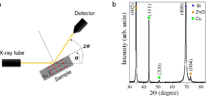
2.4 X-ray Diffraction ... 48
2.5 UV Visible Near-Infra Red (UV-VIS-NIR) Spectroscopy ... 50
2.6 Ellipsometry ... 53
2.7 Photoluminescence spectroscopy ... 54
2.8 Scanning Electron Microscopy ... 56
2.9 Transmission Electron Microscopy and Electron Energy Loss Spectroscopy ... 57
2.10 X-ray Photoelectron Spectroscopy ... 61
2.11 Hall Effect and 4-point Probe Method ... 63
2.12 Conductive Atomic Force Microscopy ... 64
2.13 Current-density Characteristics ... 66
3 Local Structure and Point-Defect-Dependent Area-Selective Atomic Layer Deposition of Copper Oxide and Metallic Copper Thin Films ... 71
3.1 Introduction ... 73
3.2 Microstructure and Morphology of the Cu2O and Cu Thin Films ... 75
3.3 Temperature-driven Selective Deposition of Cu and Cu2O on α-Al2O3 ... 81
3.4 Cu2O Deposition on Monocrystalline ZnO Substrates ... 85
3.4.1 ZnO Polar Surfaces ... 86
3.4.1 ZnO Non-Polar Surfaces ... 89
3.5 Mechanism for the Area-Selective ALD of Cu2O and Cu ... 90
3.6 Fabrication of p-Cu2O/n-ZnO Microjunctions ... 95
3.6.1 Electrical Characterization of the Microjunctions ... 98
3.7 Chapter Conclusions ... 100
4 Tunable Localized Surface Plasmon Resonance and Broadband Visible Photoresponse of Cu Nanoparticles / ZnO Surfaces ... 103
XV
4.2 Evolution of the NP with the Number of ALD Cycles ... 106
4.3 Metallic Cu Thin Film ... 109
4.4 Localized Surface Plasmon Resonance ... 110
4.5 Cu/ZnO Schottky Diode ... 113
4.6 Photo-response of Cu NP under Visible Light ... 114
4.7 Preliminary Results on the Deposition of Cu NP on ZnO Nanowires ... 119
4.8 Chapter Conclusions ... 121
5 Fabrication of Semi-Transparent p-Cu2O/n-ZnO Thin Film Heterojunctions for Photovoltaics and Photo-detecting Applications ... 123
5.1 Introduction ... 125
5.2 Structural, Morphological and Chemical Characterization ... 126
5.3 Optical Characterization of the Cu2O and ZnO Films ... 129
5.4 Electrical Characterization of the Films ... 132
5.5 Electrical and Optical Characterization of the Heterojunctions ... 133
5.6 Characterization of the Sputtered Cu2O films ... 138
5.7 Improving the Electrical Properties of the Heterojunction ... 138
5.8 Preliminary Results in the Cu2O Deposition on ZnO Nanowires ... 142
5.9 Chapter Conclusions ... 145
Conclusions and Outlook ... 147
Appendixes ... 153
Bibliography ... 157
Resume ... 180
Publications ... 181
1
Motivation
Area-selective atomic layer deposition has attracted much attention in recent years due the possibility of achieving accurate patterning with nanoscale precision, even for 2D and 3D nanostructures [1]. The area-selective growth is achieved in most cases by deactivating part of the substrate by certain molecules or by self-assembly monolayers (SAMs)[2], prior to atomic layer deposition (ALD), which results in the localized growth of the desired material in specific areas of the substrate. With the continuous downscaling of electronic devices, it is critical to develop new methods for achieving simultaneously selective deposition of different materials on different surfaces through bottom-up procedures. In this thesis we propose a novel approach to achieve area-selective deposition, that is based on the modulation of the substrate properties (in this case the conductivity/density of majority point defects in ZnO and Al-doped ZnO films) to allow local growth of different materials (Cu and Cu2O).
Plasmonic metallic nanostructures have also gained a lot of attention in recent years, due to the strong coupling between light and the free conduction electrons at the metallic nanostructures. By controlling the nanostructure size, shape and dielectric environment, light can be manipulated, focused and guided in exceptional manners. Plasmonic devices can serve as antennas to create strong localized electric fields, as waveguide to guide the light with nanoscale precision, as resonant light scatterers, as biosensor, among others. In combination with semiconductor materials, they can work as light trapping centers, enhancing considerably the photogeneration of carriers or they can directly inject carriers into the semiconductor band gap by hot-carrier generation at the nanostructure surface and transfer to the semiconductor. This phenomenon has been exploited for the fabrication of multiple optoelectronic devices, such as photodetectors, photocatalysts, optical antennas and solar cells [3–5]. Particularly, in this thesis we will show the potentialities of plasmonic Cu nanoparticles deposited by ALD on ZnO for visible photodetection.
Cu2O has sparked renewed interest in the scientific community due to its p-type
conductivity and high absorption combined with the abundance of constitutive elements in the earth crust, non-toxicity, and low-cost, which makes it compatible with low-cost all-oxide photovoltaics. Furthermore, theoretical power conversion efficiencies of ~20 % have been predicted for Cu2O-based solar cells [6]. Maximum efficiency achieved so far is of 8.1 % [7],
which means that there is still plenty of room for improvement. Among the possible n-type materials for partner layer, ZnO seems to be a suitable candidate regarding its wide band gap,
2
good electrical properties, and the compatibility with low-cost applications in combination with Cu2O. Furthermore, Cu2O/ZnO devices can find application in multiple fields such as all-oxide
photovoltaics, semi-transparent electronics, photodetection, among others [8,9]. In the last chapter of this thesis, we will present the results on the fabrication of semi-transparent Cu2O/ZnO heterojunctions by ALD and reactive magnetron sputtering.
Overall, this thesis deals with the selective deposition of Cu2O, and metallic Cu by atomic
layer deposition on ZnO substrates for applications in optoelectronics. The manuscript is organized in 5 Chapters, followed by the Conclusions and Outlook section.
Chapter 1 is a general introduction, where the basic properties of Cu2O and ZnO are
presented, followed by their applications in all-oxide photovoltaics. The second part of this chapter is devoted to the metallic plasmonic nanoparticles and their applications, as a preamble for the introduction of hot-carrier photodetectors.
Chapter 2 is dedicated to the basic principles of atomic layer deposition (ALD) and
reactive magnetron sputtering methods, employed for the deposition of Cu2O, metallic Cu,
ZnO, and Al-doped ZnO (AZO) films, together with the structural, optical, electronic and electrical characterization methods employed through this thesis.
Chapter 3 is devoted to the selective deposition of Cu and Cu2O thin films on ZnO, AZO,
and α-Al2O3 substrates. Both temperature-driven and substrate-driven selectivities are reported,
and the mechanisms behind are discussed. Particularly, for Cu2O films, the influence of the
substrate crystallographic orientation on the film growth is analyzed. Finally, Cu2O/ZnO/AZO
microjunctions were fabricated thanks to the area-selective atomic layer deposition process, and the electrical characterization of the junction is presented.
Chapter 4 is dedicated to the results on the fabrication of plasmonic Cu nanoparticles and
Cu thin films by atomic layer deposition on ZnO substrates. An evolution from Cu nanoparticles at lower number of ALD cycles to Cu films at higher number is reported. The optical characterization of the Cu nanoparticles was performed by spectroscopic ellipsometry, allowing to identify the existence of a localized surface plasmon resonance (LSPR) band. The causes of the LSPR red-shift observed for Cu NP obtained at different number of ALD cycles are discussed. Finally, the electrical properties of Cu NP/ZnO device are investigated by conductive atomic force microscopy, and the mechanism responsible for the visible photoresponse of the device is discussed.
Chapter 5 is dedicated to the fabrication and characterization of semi-transparent
heterojunctions based on Cu2O and ZnO thin films. The optical characterization of the films
3 was done through 4-point probe and Hall-effect methods. The heterojunction performance was studied by macroscopic electrical measurement in dark and under 1 Sun illumination, and the average transmittance was calculated from the transmittance spectrum in the visible region.
5
Chapter 1
1
General Introduction
In this chapter, some key elements regarding the main results obtained in this thesis are presented. The basic properties (structure, defects, electrical and optical properties, etc.) of Cu2O and ZnO thin films are discussed, together with the deposition methods employed for
their fabrication. This is followed by a description of the applications of metal oxide semiconductors in all-oxide photovoltaics, and particularly the Cu2O/ZnO-based
heterojunctions. The second part of this chapter is devoted to plasmonic nanoparticles and photodetection mechanisms. First, the main applications of plasmonic nanostructures are presented, emphasizing those related with localized surface plasmon resonance (LSPR). Secondly, some basic ideas of photodetection are discussed as a preamble for the introduction of the hot-carrier plasmonic photodetectors.
Contents
1 General Introduction ... 5 1.1 Basic Properties of Cu2O ... 6
1.1.1 Atomic Layer Deposition of Copper Oxide Thin Films... 9 1.2 Basic Properties of ZnO ... 11 1.3 All-oxides Photovoltaics ... 13 1.3.1 Cu2O-based Solar Cells ... 14
1.3.2 Cu2O/ZnO Heterojunctions ... 16
1.4 Noble Metal Nanoparticles ... 18 1.4.1 Localized Surface Plasmon Resonance ... 18 1.4.2 Effects of Size, Shape and Interparticle Distance on the LSPR Signal ... 20 1.4.3 Hot-electron Generation ... 21 1.5 Photodetectors ... 23 1.5.1 Hot-carrier Photodetectors ... 26
6
1.1 Basic Properties of Cu2O
Copper I oxide (Cu2O) is a stable binary copper compound that crystalizes in a cubic
structure (cuprite, space group Pn-3m) with lattice constant of 4.269 Å. The unit cell contains 4 copper atoms and 2 oxygen atoms. The copper atoms (blue balls) are arranged forming a face-centered-cubic sublattice and the 2 oxygen atoms (red balls) are forming a body-face-centered-cubic sublattice, as is depicted in Figure 1.1. Each oxygen atom is 4-fold coordinated with oxygen atoms and each copper atom is linearly coordinated with the two oxygen atoms, the bond lengths are indicated in Figure 1.1 [10].
Cu2O is a direct forbidden band gap semiconductor (𝐸𝑔 = 2.1 at 4.2 𝐾) with large exciton
binding energy of 150 meV [11]. In recent years, there has been a renewed interest in Cu2O due
to the experimental observation of Rydberg excitons with a principal quantum number of 25 [12], which has opened the research on giant Rydberg interaction that is of potential interest for fundamental research in condensed matter physics, and of potential impact in quantum information technologies [13].
A schematic of the Cu2O band structure at the Γ-point of the Brillouin zone is shown in
Figure 1.2. The highest valence band (Γ7+) has a d-like character since it originates from the
3d-Cu orbital, while the lowest conduction band (Γ6+) presents a 4s-like character and originates
from the 4s-Cu orbital. The transitions from the valence band to the conduction band are represented in Figure 1.2, and, from their associated emission wavelength, they are named: yellow (Γ7+ → Γ
6+, 𝐸 = 2.173 𝑒𝑉), green (Γ8+ → Γ6+, 𝐸 = 2.304 𝑒𝑉), blue (Γ7+ → Γ8−, 𝐸 =
2.625 𝑒𝑉) and indigo (Γ8+ → Γ
8−, 𝐸 = 2.756 𝑒𝑉) [14,15]. The lowest fundamental transition is
dipole-forbidden, since the parity of the lower conduction band and the highest valence band is the same. In consequence, the yellow and green series, can only occur by a phonon-assisted process, and the lowest allowed optical transition are the blue and the indigo series. This is the Figure 1.1. Crystal structure of cuprite Cu2O (space group Pn-3m). The bond lengths are indicated.
7 reason why experimentally optical bandgap values ranging from 2.4 to 2.7 eV have been reported for Cu2O [16].
Regarding the electrical properties, Cu2O films exhibit intrinsic p-type conductivity. From
theoretical studies and by deep-level transient spectroscopy analysis, it has been determined that the possible defects contributing to p-type conductivity in Cu2O are: single Cu vacancies,
VCu, copper vacancies in the split configuration, V Cu split (a copper interstitial, Cu i, between two VCu) [18], and oxygen interstitials Oi in tetrahedral (O i tet) or octahedral (O i oct) coordination
(Figure 1.3). Among them, the single VCu and the V Cu splitconfiguration have the lowest formation
energy under both, Cu-rich and Cu-poor conditions (see Figure 1.3), with transitions levels 𝜖(0/−) at 0.22 and 0.47 eV above the valence band maximum, respectively [19], in agreement with the experimental values of 0.2 and 0.5 eV, obtained by deep-level transient spectroscopy [20]. On the other hand, Oi defects have much higher formation energies and are located deeper in the bandgap. Therefore, Oi defects don’t contribute to the p-type conductivity, which arises mainly from VCu and V Cu split.
The influence of extrinsic defects in Cu2O has also been studied. For example, nitrogen
doping results in the formation of a shallow acceptor level associated to the molecular N2
substituting Cu, (N2)Cu, that enhances hole carrier concentration and Cu2O conductivity [21].
H-related defects have also been analyzed, and the complex H-VCu (that results from the Figure 1.2. Schematic of the Cu2O band structure at the 𝚪-point of the Brillouin zone, the different
electronic transitions leading to the four excitonic series are indicated. Origin of conduction and valence bands from the atomic orbitals and the band splitting considering crystal-field and spin-orbit interaction are depicted on the right [17].
8
interaction between an hydrogen atom and a VCu presents low formation energy (0.17 eV), with transitions levels 𝜖(0/−) at ~ 1.15 𝑒𝑉, very deep inside the band gap. Therefore, this type of defect mainly works as hole killer, affecting p-type conductivity in Cu2O [22].
Several techniques have been used for the deposition of Cu2O like sputtering [23], pulsed
laser deposition [24,25], electrochemical deposition [26], molecular beam epitaxy, chemical vapor deposition, and atomic layer deposition (ALD) [27,28]. The electrical properties of Cu2O
are very sensitive to deposition method, since the Cu2O stoichiometry and point defect densities
evolve from one technique to other. In fact, the resistivity, carrier concentration and carrier mobility reported in the literature, change widely depending on the growth conditions. Cu2O
films deposited by thermal oxidation show resistivity values ranging from 102− 104 Ω cm [29]. For electrodeposited films, even higher values have been reported around 104− 106 Ω cm, with low hole carrier concentrations of 1013− 1014 𝑐𝑚−3, and mobilities of
~1 𝑐𝑚2⁄ [29,30]. Lower resistivity values have been reported for sputtered Cu𝑉𝑠
2O films
ranging from 10 to 103 Ω cm, with higher hole concentrations of 1016− 1017 𝑐𝑚−3, and carrier mobilities of 1 − 62 𝑐𝑚2⁄ [16,31], which make this technique effective for the 𝑉𝑠 fabrication of Cu2O films, with good electrical performance. Recently, ALD has emerged as a
successful approach to deposit high quality Cu2O thin films, with the additional advantage of
producing highly uniform and conformal films. D. Muñoz-Rojas et al. reported the fabrication of low resistivity (125 Ω cm) Cu2O thin films (~100 nm) deposited at relatively low temperature
(225 °C) by atmospheric pressure spatial ALD, with hole mobilities and carriers concentrations of 5 𝑐𝑚2⁄ and 10𝑉𝑠 16 𝑐𝑚−3, respectively [28]. High carrier mobility of 8.05 𝑐𝑚2/𝑉 𝑠 has Figure 1.3. Theoretical calculations of the formation energy for the different acceptor levels in Cu2O,
under Cu-rich (left) and Cu-poor (right) conditions (color lines). The vertical dashed lines represent experimental values obtained from deep-level transient spectroscopy measurements [19].
9 also been reported for Cu2O thin films deposited by thermal ALD, however the films presented
lower carrier concentrations of 5.88 × 10¹⁴ 𝑐𝑚−3 [27].
High mobility and carrier concentrations of at least 1016 𝑐𝑚−3, are required for the applications in the TCO industry, and also to achieve good performance in photovoltaics. In this sense, sputtering and ALD appear to be promising for the fabrication of Cu2O-based
devices.
1.1.1 Atomic Layer Deposition of Copper Oxide Thin Films
Atomic layer deposition has emerged as a successful technique for the growth of high quality thin films, with high uniformity and high degree of conformability. The self-limiting growth mechanism in which ALD is based allows a very precise thickness control and a conformal deposition on high aspect-ratio structures, which is highly demanded in the microelectronics industry due to the continuous miniaturization trend in semiconductor devices. ALD found its first application in the thin film electroluminescent displays (TFEL) industry, since high-quality luminescence films deposited on large area substrates were required [32], and where it is widely used to the present days. Furthermore, ALD is commercially used in the semiconductor industry for the fabrication of high-k dielectrics like Al2O3, ZrO2, and HfO2 for
metal–oxide semiconductor field-effect transistors (MOSFET), capacitors for dynamic random access memory (DRAM), and, in general, for complementary metal-oxide semiconductor (CMOS) technology [33]. ALD processes have been developed for the fabrication of metal and nitrides for electrodes and interconnects [32]. Recently, ALD has also been applied in photovoltaic technology for the fabrication of electrodes, transparent conductive oxides, thin-film semiconducting layers, passivation layers, and moisture diffusion barrier in organic solar cells [33–35].
There are many reports regarding the deposition of metallic Cu film by ALD [36–40], mainly for applications in microelectronics interconnection. In contrast, the deposition of copper oxides by ALD has been considerably less studied, and it started to gain interest in recent years due to the potentialities of Cu2O for all-oxides photovoltaic applications.
Different approaches have been employed for the deposition of Cu2O films. T. Törndahl
reported the deposition of Cu2O thin films on amorphous SiO2 and single crystalline α-Al2O3
substrates by a high-temperature thermal ALD process (from 350 to 700 °C), using copper (I) chloride and water as precursors [41]. The films deposited were polycrystalline on SiO2 and
showed a (110) texture in α-Al2O3, more pronounced at higher temperatures. However, they
10
at higher deposition temperatures. They also reported a lower temperature ALD process (210 - 300°C) when using a different precursor, copper (II) hexafluoroacetylacetonate, Cu(hfac)2. This
precursor was employed for the growth of Cu3N films in a six-steps ALD process, using water
and ammonia as reactants [42], and Cu2O films were formed when the ammonia pulse was
removed. A two-step process was reported by Kwon et al., consisting on the growth of metallic Cu using hexafluoroacetylacetonate Cu(I) (3,3-dimethyl-1-butene) and a H2 plasma followed
by oxidation in an O2 plasma. This method allows the selective deposition of Cu, CuO and
Cu2O by changing the number of Cu deposition steps [43]. Highly-conformal Cu2O films were
also deposited by bis(1–dimethylamino–2–methyl–2–butoxy) copper (C14H32N2O2Cu), and
H2O in an ALD temperature window ranging from 120 to 240 °C [27]. Copper acetylacetonate,
Cu(acac2), was employed as copper precursor in combination with ozone (O3) from depositing
the tenorite phase of copper (II) oxide films [44]. Muñoz-Rojas et al. obtained high mobility Cu2O film by atmospheric pressure spatial ALD, using (Trimethylvinylsilyl)
hexafluoroacetylacetonato Copper(I), Cu(I)(hfac)(TMVS), as copper precursor and water as oxidizer [28].
In this thesis we will demonstrate the deposition of high quality Cu2O thin films by thermal
ALD, using Cu(hfac)2 as copper precursor and water as oxidizer. The films grown by this
method present excellent electrical properties with high mobility and low resistivity. Furthermore, temperature-driven and conductivity-driven selective deposition processes will be demonstrated on different substrates, which allow the deposition of both metallic Cu and Cu2O thin films.
11
1.2 Basic Properties of ZnO
ZnO is a n-type transparent conductive oxide (TCO) with a wide band gap of 3.37 eV, large exciton binding energy of 60 meV, high electron mobility, high thermal conductivity, and strong piezoelectric responses [45]. Furthermore, it is available as high-quality single crystal, and can be easily fabricated in different nanostructured architectures [46]. These properties make it an ideal candidate for UV photodetection, light emitting diodes, transparent thin film transistors, sensors, and window layers in solar cells [47–50].
At ambient conditions ZnO crystalizes in the wurtzite hexagonal crystal structure (space group P63mc), with lattice parameter 𝑎 = 3.25 Å and 𝑐 = 5.21 Å (see schematic in Figure
1.4). This structure is the superposition of two hexagonal-close-packed (hcp) sublattices of Zn and O. The zinc atoms are connected with oxygen atoms in tetrahedral coordination and vice versa.
Due to its large band gap of 3.37 eV, ZnO is transparent in the visible range of the electromagnetic spectrum. It is a direct band gap semiconductor since the valence band maximum and the conduction band minimum are located at the same k-point (Γ-point of the Brillouin zone), as can be seen in Figure 1.5 A. The conduction band arises mainly from the empty 4s states of Zn2+, meanwhile the highest valence band arises from the occupied 2p states of O2- [51].
Several native point defects have been identified in ZnO crystals: oxygen vacancies (VO), zinc vacancies (VZn), oxygen interstitials (Oi), and zinc interstitials (Zni), among others. Most of the calculations agree that VO has the lowest formation energy among all the ZnO defects
(~ 1 eV under oxygen-poor conditions) [52]. On the other hand, VZn have shown its lowest formation energy under oxygen-rich conditions, particularly for n-type ZnO [45]. Oi and VZn
have been considered acceptor defects in ZnO. Particularly, VZn are considered as the main
compensating centers in n-type ZnO; this was corroborated experimentally by positron annihilation spectroscopy [45]. On the contrary, Vo and Zni are both donor defects, Zni being a shallow donor (~ 0.05 eV below the conduction band), and VO a deep donor [45,52]. In n-type ZnO, Zni has a very high formation energy, however it has been suggested that this type
of defect can still be formed under out-of-stable-equilibrium conditions [53]. The intrinsic n-type conductivity of ZnO can be explained by the presence of native donor defects, however this topic is still under debate, and some authors claim that it is the result of the existence of impurities in the ZnO acting as extrinsic donor defects. In particular, interstitial hydrogen (Hi)
12
and substitutional hydrogen at the oxygen site (HO) have been identified as shallow donors,
with low formation energies, which means that they can exist in large amount in ZnO [45,52]. There is also the possibility of intentionally doping ZnO in order to increase the carrier concentration. Potential candidates for n-doping are the elements of group III B, that substitute the Zn cation site, such as Al, Ga, B or In. These elements have one additional valence electron compared to Zn, and therefore they introduce an extra electron into the ZnO conduction band [54,55]. The elements of group VII like Cl, F or I, can also act as donor dopants, in this case by substituting the oxygen atom, and providing also an extra electron into the conduction band [56]. Al has been the most commonly employed dopant for ZnO, improving considerably the ZnO conductivity [57,58]. Minami et al. reported resistivity values of 2 × 10⁻⁴ Ω𝑐𝑚, and carrier concentration of ~ 1021 𝑐𝑚−3, for AZO films fabricated by RF magnetron sputtering
[59]. Resistivity of ~10−4 Ω𝑐𝑚 and carrier concentration of 11 × 1020 𝑐𝑚−3, were obtained
for Al-doped ZnO (AZO) thin films deposited by high impulse magnetron sputtering [60], and Agura et al. reported resistivity and carriers concentration of 8.5 × 10⁻⁵ Ω𝑐𝑚, and 1.5 × 10²¹ 𝑐𝑚−3, respectively for AZO films deposited by pulsed laser deposition (PLD) [61].
ZnO thin films can be grown by several techniques. Examples of the chemical routes most commonly employed are the sol-gel methods, electrochemical deposition, that has been widely employed for the growth of ZnO nanostructures [62], and chemical vapor deposition [63]. On Figure 1.5. Band structure of a ZnO perfect crystal (A), and considering different types of defects: oxygen vacancies in the neutral state (B) and 2+ charge states (C), and Zn interstitial at the octahedral site in the neutral state [52].
13 the other hand, among the physical vapor deposition methods there are: pulsed laser deposition [61], molecular beam epitaxy [64], and sputtering (DC, RF and HiPIMS) [60,65].
The sputtering technique is one of the most popular techniques employed for the deposition of ZnO thin films. It is a relatively simple method that allows the deposition of ZnO films with good electrical and optical properties, at low operating temperature, with the advantage of scalability to large-area substrates.
In this thesis we used the reactive magnetron sputtering method for the growth of ZnO and AZO films in Ar+O2 atmosphere. By changing the O2 partial pressure in the reaction chamber
it is possible to tune the conductivity of the ZnO films in a large range.
1.3 All-oxides Photovoltaics
Metal oxide semiconductors have gained a lot of attention regarding their good chemical stability, abundance of constitutive elements in the earth crust, non-toxicity and low-fabrication cost. They can find application in a wide variety of fields like optoelectronics [45], photovoltaics [8,67], water splitting [26], and photodetection [9], among others. Furthermore, the fabrication of all-oxide based devices is emerging as a promising approach to reduce manufacturing costs and environmental impact.
The photovoltaic market has experienced a spectacular growth in the last decade (Figure 1.6). In 2017 the solar global market grew by 30% with respect to the previous year, reaching a global solar photovoltaic installed capacity of 99 GW, which leads to a cumulative installed capacity of more than 400 GW. However, even with this prosperity, further improvements need to be achieved in terms of efficiency and prize reduction to render PV competitive with Figure 1.6. Evolution of the annual global photovoltaic production in the period 2010 - 2017 [66].
14
traditional electricity generation systems based on fossil fuels. In this sense, the use of low-cost, abundant and environmental-friendly materials is one of the challenges of PV technology. PV based on semiconductor oxides is a promising solution to accomplish this objective.
Metal oxide semiconductors have been already employed in solar cells technology, mainly as transparent conductor oxides (TCOs), such as indium tin oxide (ITO), fluorine-doped tin oxide (FTO), and ZnO-based materials [8]. TCOs have been widely used in the commercially available copper indium gallium diselenide (CIGS), and CdTe thin film technology [68–70], in copper indium selenide (CIS) solar cells [71] and in amorphous Si [72] technology. Two different solar cells configurations based on CdTe and CIGS absorber layers are depicted in Figure 1.7, with the use of different TCOs (ZnO, Al-doped ZnO, and ITO). The fabrication of textured or nanostructured TCOs has also been explored as a way of enhancing absorption, by light trapping and internal reflectance enhancement, and to increase carrier transport efficiency [8,73].
1.3.1 Cu2O-based Solar Cells
Most of the applied TCOs are n-type materials, and achieving p-type doping is challenging. Therefore, for the progress of all-oxide photovoltaic industry entirely based on semiconductor oxides, p-type absorber materials with as good electrical properties as their n-type counterpart, Figure 1.7. Schematic and cross-section SEM micrograph of a thin film CIGS solar cell on a flexible polyimide substrates, from [74] (a). Schematic and colored cross-section SEM micrograph of a CdTe solar cell, from [75] (b).
15 need to be developed. Among the p-type semiconductor oxides, Cu2O is a suitable candidate
due to its large absorption coefficient, high hole mobility, abundance of constitutive element in the earth crust, and non-toxicity. It has found application as p-type absorbed layer in combination with n-type wide bandgap semiconductor oxides such as ZnO, TiO2, and Ga2O3
[76–78], as hole transporter layer in perovskite solar cells [79], and it has been investigated as constitutive of the top cell of Si-based tandem solar cells in combination with ZnO [80].
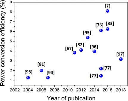
A theoretical power conversion efficiency (PCE) of 23% was predicted by the Shockley-Queisser theory [8] for Cu2O as absorber layer in solar cells. However, so far, efficiencies
reported for Cu2O based devices remain far from the theoretical value (see Figure 1.8). The
𝑉𝑂𝐶, 𝐼𝑆𝐶, 𝐹𝐹, and PCE of several Cu2O-based solar cells are reported in Table 1.1, from 2004
up to the present. Cu2O/TiO2 heterojunctions have been fabricated on FTO/glass substrates by
spray-pyrolysis. Maximum open circuit voltage (𝑉𝑂𝐶), and short-circuited current (𝐼𝑆𝐶) values
for this device were of 350 𝑚𝑉, and 0.4 𝑚𝐴/𝑐𝑚2, respectively. The authors claim that the small current density measured is not due to low absorption but to poor electrical quality of the Cu2O films [78]. Cu2O/ITO and Cu2O/ZnO/ITO devices were fabricated by Mittiga et al. [81].
The Cu2O thin films were grown by oxidation of Cu sheet at high temperatures, and the TCOs
films (ITO and ZnO) were deposited by ion beam sputtering at room temperature. Higher 𝑉𝑂𝐶
and 𝐼𝑆𝐶 values of 575 𝑚𝑉 and 6.78 𝑚𝐴/𝑐𝑚2, were obtained compared with the Cu2O/TiO2
heterojunctions. PCE of 1 and 2 % were reported for the Cu2O/ITO and Cu2O/ZnO/ITO,
respectively. The authors point out that the factor limiting the device performance is the
16
presence of high series resistance, due to the high resistivity (~1000 Ω𝑐𝑚) of the Cu2O films.
Nishi et al. reported an improvement of PCE by introducing a 50-nm ZnO buffer layer between a n-AZO and a p-Cu2O films, reaching a PCE of 4.12 %, that is the highest value reported for
a ZnO/Cu2O-based solar cells [82].
A PCE of 6.25 % was reported by Minami et al., in a MgF2/AZO/
(Ga0.975Al0.025)2O3/Cu2O:Nadevice, with 𝑉𝑂𝐶 and 𝐼𝑆𝐶 values of 840 𝑚𝑉 and 10.8 mA/cm2,
respectively [83]. The improvement of the device performance was achieved in this case by optimization of the chemical composition of the n-type oxide and optimization of the Cu2O film
resistivity through Na-doping. Minami et al. also reported a higher PCE of 8.1 %, in a similar device by replacing the multi-component oxide (Ga0.975Al0.025)2O3 by Zn0.38Ge0.62O. The
authors claim that the improvement of the PCE in this device is the result of the lower electron affinity of the new multi-component oxide employed, that allows a reduction of the conduction band offset with Cu2O.
1.3.2 Cu2O/ZnO Heterojunctions
As can be seen in Table 1.1, the Cu2O-ZnO system has been by far the most studied. Until now
we have presented some examples of Cu2O-based devices in which the thickness of the Cu2O
absorber layer ranged from 2 to 250 μm. However, there are several approaches where nanostructured devices have been fabricated to enhance the optical absorption without the need of thick absorbing layers as a way of improving charge collection, and reducing material use. Most of them consist in the deposition of Cu2O thin films on ZnO nanostructures (nanowire,
nanorods, or nanotubes), due to the versatility of ZnO to be produced in nanostructure architectures of different sizes and shapes [84–87]. Therefore, due to the high surface area of the nanostructured devices, lower thicknesses of Cu2O are required. Additionally, the distance
that carriers need to travel before reaching the junction is significantly reduced, increasing carrier collection efficiency.
Cu2O/ZnO heterojunctions have also been studied for application in low-cost transparent
electronics and transparent photovoltaics. In this type of devices, a compromise between transparency and electrical performance need to be reached. The relatively large band gap of Cu2O (higher than the optimum value of 1.34 eV, predicted by the Shockley-Queisser theory
[88]) makes it a promising candidate in this field in combination with ZnO [89–91]. Furthermore, Cu2O/ZnO heterojunctions have been explored as possible candidates for
photodetection [86], particularly in nanostructured architectures. High-performance in UV-VIS photodetection was reported in a device made of single-wall carbon nanotubes (SWNTs)/PET
17 substrates covered by ZnO/Cu2O hybrid nanofilm, deposited by RF magnetron sputtering [92],
and recently, a fast response self-powered photodetector was reported in a ZnO/Cu2O core-shell
nanowires device [9].
In this thesis we will present the results on the fabrication of transparent thin film ZnO/Cu2O heterojunctions. The Cu2O films were deposited by ALD, since it allows achieving
high mobility and low resistivity values which is essential to improve carriers transport properties. Furthermore, a good interface matching is obtained between the Cu2O and ZnO
films, which is particularly important to achieve an efficient charge separation and improve the device performance.
Table 1.1. Cu2O-based photovoltaic devices, electrical performance up to 2018. Growth method Heterojunctions VOC (V) JSC (mA/cm2) FF (%) PCE (%) Ref. PLD / TO AZO/Cu2O 0.4 7.1 0.4 1.28 [93] IBS / TO ITO/ZnO/Cu2O 0.59 6.78 50% 2 [81] ECD ZnO/Cu2O 0.41 7.1 42 1.28 [94] PLD / TO AZO/ZnO/Cu2O 0.69 10.1 55 3.83 [67] PLD / TO AZO/ZnO/Cu2O 0.72 9.67 58 4.12 [82] PLD / TO AZO/Ga2O3/Cu2O 0.8 9.99 67 5.38 [95]
ALD / ED AZO/Ga2O3/Cu2O 1.2 7.37 44.7 3.97 [96]
AALD / TO ITO/Zn0.79Mg0.21O/Cu2O 0.65 6.9 49.2 2.2 [77]
AALD / TO ITO/ZnO/Cu2O 0.49 7.5 40 1.46 [77] PLD / TO AZO/Al0.025Ga0.975O/ Cu2O:Na 0.84 10.95 66 6.1 [76] PLD / TO AZO/(Al0.025Ga0.975)2O3/ Cu2O: Na 0.84 10.8 69 6.25 [83] PLD / TO AZO/Zn0.38Ge0.62O/ Cu2O:Na 1.1 11.1 62 8.1 [7] RO/RPE-CVD ZnO/Cu2O 0.557 11.42 49.8 3.17 [97]
TO, thermal oxidation; PLD, pulsed laser deposition; IBS, ion beam sputtering; ECD, electrochemical deposition; ALD, atomic layer deposition; AALD, atmospheric ALD; RO, radical oxidation; RPE-CVD, remote-plasma-enhanced chemical vapor deposition.
18
1.4 Noble Metal Nanoparticles
Noble metal nanoparticles have attracted lot of attention for mankind since prehistoric times, particularly gold and silver, which were used mainly for artistic and decorative purposes, for example, in the coloration of glasses, ceramics, fabric, etc. Today the comprehension of the atomic world, and the technological advances in nanofabrication techniques, have opened an avenue toward new applications that allow the precise control and manipulation of light, through the metal nanostructures that can be effectively used to focus and guide the light with nanoscale precision. By controlling the size, shape, chemical composition, and agglomeration of the nanoparticles, their chemical, optical and electrical properties can be manipulated, finding application in multidisciplinary fields such as, catalysis, optoelectronics, bio-sensing, photovoltaics, among others [98–101].
1.4.1 Localized Surface Plasmon Resonance
Metallic nanoparticles exhibit localized surface plasmon resonance (LSPR), that is the collective oscillation of the valence electrons at the metallic nanoparticle that enters in resonance with an external electromagnetic field, resulting in a selective absorption of light at the resonance plasmon frequency, and the enhancement of the electromagnetic field at the particle surface (see Figure 1.9).
Gustave Mie was the first to provide a theoretical background for explaining the plasmon resonance phenomenon observed in noble metal nanoparticles, by solving Maxwell equations on a metallic sphere of radius R, under the action of an electromagnetic field [102]. When the wavelength (𝜆) of the incident light is much higher that the particle radius (𝑅 𝜆⁄ < 0.1), only
![Figure 1.9. Schematic of localized surface plasmon resonance at the metallic nanoparticles [98]](https://thumb-eu.123doks.com/thumbv2/123doknet/14721193.751182/38.892.166.729.816.1051/figure-schematic-localized-surface-plasmon-resonance-metallic-nanoparticles.webp)
![Figure 1.17. SEM micrograph of an hybrid photodetector made of Au nanorods on ZnO nanowires (left), the photocurrent of the hybrid device (red) and of the virgin ZnO nanowires (blue) as a function of the wavelength (right), modified from [5] (a)](https://thumb-eu.123doks.com/thumbv2/123doknet/14721193.751182/48.892.120.784.132.602/micrograph-photodetector-nanorods-nanowires-photocurrent-nanowires-function-wavelength.webp)
![Figure 2.5. Evolution of the GPC with the number of ALD cycles. Linear growth (a), substrate- substrate-enhanced growth (b), substrate-inhibited growth type I, and substrate-inhibited growth type II (d) [121]](https://thumb-eu.123doks.com/thumbv2/123doknet/14721193.751182/58.892.194.696.106.457/evolution-substrate-substrate-enhanced-substrate-inhibited-substrate-inhibited.webp)