RESEARCH OUTPUTS / RÉSULTATS DE RECHERCHE
Author(s) - Auteur(s) :
Publication date - Date de publication :
Permanent link - Permalien :
Rights / License - Licence de droit d’auteur :
Bibliothèque Universitaire Moretus Plantin
Institutional Repository - Research Portal
Dépôt Institutionnel - Portail de la Recherche
researchportal.unamur.be
University of Namur
Study of ZrN layers deposited by reactive magnetron sputtering
Del Re, M.; Gouttebaron, R.; Dauchot, J.P.; Leclere, P.; Terwagne, Guy; Hecq, M.
Published in:Surface and Coatings Technology
Publication date: 2003
Document Version Peer reviewed version
Link to publication
Citation for pulished version (HARVARD):
Del Re, M, Gouttebaron, R, Dauchot, JP, Leclere, P, Terwagne, G & Hecq, M 2003, 'Study of ZrN layers deposited by reactive magnetron sputtering', Surface and Coatings Technology, vol. 174-175, pp. 240-245.
General rights
Copyright and moral rights for the publications made accessible in the public portal are retained by the authors and/or other copyright owners and it is a condition of accessing publications that users recognise and abide by the legal requirements associated with these rights. • Users may download and print one copy of any publication from the public portal for the purpose of private study or research. • You may not further distribute the material or use it for any profit-making activity or commercial gain
• You may freely distribute the URL identifying the publication in the public portal ?
Take down policy
If you believe that this document breaches copyright please contact us providing details, and we will remove access to the work immediately and investigate your claim.
0257-8972/03/$- see front matter䊚 2003 Elsevier Science B.V. All rights reserved. doi:10.1016/S0257-8972Ž03.00679-0
Study of ZrN layers deposited by reactive magnetron sputtering
M. Del Re *, R. Gouttebaron , J.-P. Dauchot , P. Leclere , G. Terwagne , M. Hecq
a, a a`
b c aLaboratoire de Chimie Inorganique et Analytique, Universite de Mons-Hainaut, Parc Initialis, Av. Copernic 7000 Mons, Belgium
a ´
Service de Chimie des Materiaux Nouveaux, Universite de Mons-Hainaut, Parc Initialis, Av. Copernic 7000 Mons, Belgium
b ´ ´
Laboratoire d’Analyse par Reactions Nucleaires, FUNDP, Rue de Bruxelles, 61 5000 Namur, Belgium
c ´ ´
Abstract
Zirconium nitride films are deposited onto borosilicate wafers by reactive magnetron sputtering. The films are analysed in situ by X-ray photoelectron spectroscopy(XPS). We have studied by XPS the effects of the nitrogen partial pressure (1–100%), the subtract temperature(ambient to 450 8C), and biasing (0–80 W) on the stoichiometry of ZrN films. The N1s peak is composed of three components at 397.2, 396.4 and 395.8 eV in binding energy. These components are correlated with the three existing phases of zirconium nitride(ZrN, Zr N and ZrN ). With an increase of the nitrogen partial pressure, a shift of the Zr3d line to3 4 2
the high binding energy and the increase of the N1s component at 395.8 eV are observed. These observations are explained by the charge transfer between Zr to N which increases with P(N ) as previously described for the Ti–N system w1x. The bulk2 2
stoichiometry is calculated by Rutherford backscattering and nuclear reaction measurements. The resistivity of the films is measured by the four-point probes technique. The reflectivity of the films are recorded by a spectrophotometer in the IR–Vis range. A correlation between the reflectivity and the resistivity is observed. The roughness of the films is measured by atomic force microscopy. The bias voltage has a great influence on the surface roughness and on the reflectivity of the films. The dependence of the ZrN films structure and morphology with the discharge parameters is established.x
䊚 2003 Elsevier Science B.V. All rights reserved.
Keywords: XPS; RBS; Reactive magnetron sputtering; ZrN
1. Introduction
The thermal insulation techniques of windows have been enhanced due to the development of thin films sputter deposition. ZrN is known to be a good reflective material in the IR wavelength range w2x. It is due to the metallic structure of the stoichiometric ZrN. This prop-erty is interesting for applications in thermal insulation coatings. Thin films are deposited by various methods: evaporation, spray pyrolysis, chemical vapour deposition and sputtering. In the present work, we study the sputtering of a zirconium target in a mixture of AryN2 direct current magnetron discharges. X-ray photoelectron spectroscopy (XPS), Rutherford backscattering (RBS) and NRA are used to characterize the composition of the films. The resistivity is given by the four points probe technique. The reflectivity of the films are record-ed in the IR–Vis range. The roughness of the films is measured by atomic force microscopy(AFM). We have *Corresponding author. Tel.: 38-51; fax: q32-65-37-38-41.
E-mail address: [email protected](M. Del Re).
correlated the shapes and positions of the XPS peaks with the stoichiometries of the ZrN films.x
2. Experimental details
The ZrN films are deposited by d.c. reactive magne-tron sputtering. The target–substrate distance is 15 cm. The substrate is a borosilicate glass of 1 cm cleaned2 with a Balzers substrate cleaner 1 and 2. The experi-mental system is described elsewhere w3x. The low pressure is obtained by means of a turbomolecular– diaphragm pump combination. The ultimate vacuum pressure is approximately 10y7 Torr. The sputtering gas is an argonynitrogen mixture and the pressure is
regu-lated with a throttlevalve. The gas inlet is situated in front of the substrate holder. Two gas flow controllers maintain the argon and nitrogen flows in the chamber. A continuously variable power supply MDX 500 is used as the power source. The target current is set at 200 mA. The target voltage is fluctuating (f250 V) with the nitrogen partial flow. Zirconium disk(99.2% purity) of 1.3 inch in diameter is used as target. The deposition
Fig. 1. Stoichiometry vs. P N .2
Fig. 2.(a) ZrN without bias, profile, after air contamination; (b) ZrN with bias, profile, after air contamination.
rate is measured using a quartz microbalance. All the experiments have been performed under UHV, there is no air contamination of film surfaces before XPS anal-ysis. The samples are transferred under UHV into an ESCA analysis chamber. XPS was performed on a VG-ESCALAB 220iXL spectrometer. The pressure in the analysis chamber was typically 8=10y11 Torr. Atomic composition were derived from peak areas by using photoionisation cross section calculated by Scofield w4x, corrected for the dependence of the escape depth on the kinetic energy (KE) of the electrons (assumed to have
the form lsKE0.6) and corrected for the analyser
transmission function of our spectrometer. The diameter of the Al Ka X-ray beam is 250 mm. The scan number for each XPS area corresponding to all the film elements varies from 10 to 15. RBS and NRA measurements were performed on the Tandetron´ 娃 2 MV (ALTAIS) at¨ the LARN. For RBS measurements, the energy of the incident particles( He ) is 2.0 MeV. This technique is4 2q suitable for the quantification of heavy atoms like Zr. Otherwise, for the NRA measurement, the energy of the incident particles is raised to 4.8 MeV. This technique is preferred for the quantification of light atoms like N
or O. Simulated curves are compared to the experimental ones to quantify the atomic composition of the films. AFM measurements were performed on a Nanoscope IIIa microscope in the tapping mode. The root mean square (RMS) deviation are calculated from several pictures taken on each sample w10x. This measure is assimilated to the roughness of the film surface. The analysed surface is varied from 25 to 1 mm .2
3. Results and discussion 3.1. Stoichiometry
We have studied ZrN coatings deposited at room temperature under different nitrogen partial pressure(1–
100%). The total pressure is fixed at 8 mTorr. The ZrN
films are synthesized with and without bias voltage of
y200 V and analysed by XPS. Whatever the
experi-mental conditions may be, oxygen traces are detected on the films surfaces (f4% at.) and on the bulk films
(f2% at.). This low oxygen contamination of the films
can be explained by the extreme reactivity of Zr in relation to H O still present as traces in the residual gas2 phase of the preparation and transfer chambers (10y7 Torr). The results are shown on Fig. 1. Without bias,
the ratio NyZr is under 1 until 15% of nitrogen and
goes to 1.07 at 100%. The addition of a bias of 200 V induces a decrease of the ratio. It stays under 1 for all the nitrogen partial pressure. It is due to the preferential sputtering of the nitrogen in the growing film. We have realized an XPS depth profile of ZrN films synthesized with and without bias voltage and after air contamination
(Fig. 2a and b). We can observe that the films
synthe-sized without any bias are oxidised through all the bulk. The final stoichiometry reaches ZrN O . On the other0.5 0.5 hand, the films synthesized with bias contents only 6% of oxygen in the bulk. It is due to the porosity decrease of the films when bias is added during deposition. The oxygen diffusion in the bulk film is decreased.
The N1s XPS spectrum shows three components at 397.1 eV(1) in binding energy, 396.4 eV (2) and 395.8
Fig. 3. N1s peak fit.
Table 1
Bulk stoichiometries of the ZrN films obtained by RBS and NRA Ech. PN2(%) Bias (V) Zr (%) N (%) O (%) Stiochio princ
1 1 250 46 46 7 ZrN 2 3 250 50 47 2 ZrN 3 50 250 43 51 4 ZrN1,2 4 100 250 30 57 13 ZrN2 5 1 0 36 34 30 ZrNO 6 3 0 36 32 32 ZrNO 7 50 0 36 60 4 ZrN2 8 100 0 35 60 5 ZrN2
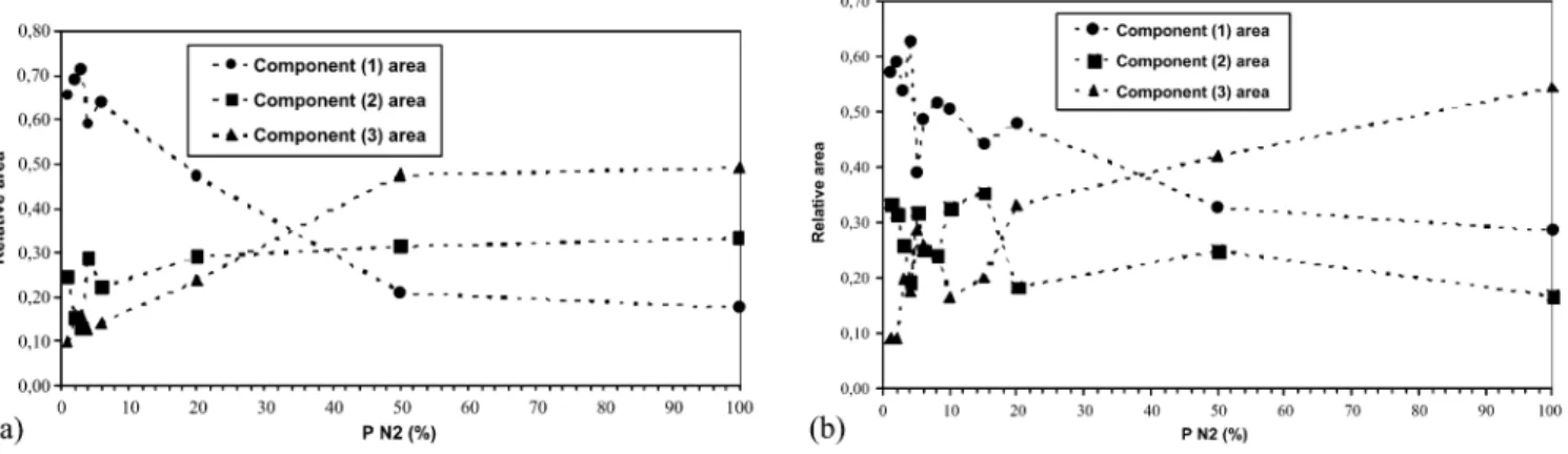
Fig. 4.(a) Quantification of the N1s XPS peak, film synthesized with bias; (b) quantification of the N1s XPS peak, film synthesized without
bias.
eV (3) (Fig. 3: at 4% N2, y200 V bias). In some
papers w1,2x, the component(1) is attributed to the ZrN
stoichiometry while the component (2) is attributed to
zirconium oxynitride w5x. But in an other paper w6x, the component(2) corresponds to the Zr N stoichiometry.3 4 The component (3) could be attributed to an
over-stoichiometry like ZrN . We have followed the evolution2 of these three components areas with the increase of the nitrogen partial pressure in films synthesized with bias and without bias (Fig. 4a and b, respectively). These evolutions are quite different depending on whether the deposition is done with or without bias voltage. In both cases, the area of the component(1) is higher than the others until a nitrogen partial pressure of 40%. On the other hand, the area of the component (2) increases
only with bias voltage. At 100% of nitrogen, the ratio between area(3) and (1) is almost 3 with bias while it
is under 2 without bias. The components (2) and (3)
correspond to phases which appear when the sputtered atoms arriving on the film surface receive an energy supply thanks to the bombardment of the growing film by positive ions (Ar , N ). These two componentsq q
2
could correspond to the over-stoichiometric metastable phases of the ZrNx (Zr N and ZrN ). A chemical shift3 4 2 to the high binding energy of the Zr3d XPS peak with
the nitrogen partial pressure increases has been observed
(Fig. 5). The Zr3d peak goes from 179.6 eV at 1% of
nitrogen partial pressure to 180.6 eV at 100%. These kind of shift has already been observed for TiN films sputtered by Nq ions w1x. The absence of the oxyde
2
components in the Zr3d peaks(located at 182.2 eV and 184.6 eV in binding energy) turns down the oxynitride
hypothesis. From the XPS results, zirconium nitride films synthesized with bias voltage are made of over stoichiometric metastable phases(Zr N , ZrN ). But the3 4 2 atomic composition derived from peak areas(calculated
by the method describes at point 2) shows that nitrogeny
zirconium ratio is always lower than 1. In order to understand this result, the stoichiometry of the films has been measured using another techniques, RBS and NRA
w7x. The combination of these techniques gives the
stoichiometry of the films which varies from ZrN to ZrN when the N percentage increases from 1 to 100%2 2
(Table 1).
The under-estimated stoichiometry results obtained by XPS can be explained by the approximation of the electron mean free path to KE0.6 from the universal curve(at 1 KE, strong variations of l depending on the nature of the analysed components), the sensitivity factor used (Scofield rather than Wagner). This point has still to be improved.
Fig. 5. Chemical shift of the Zr3d XPS peak with nitrogen.
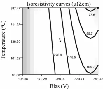
Fig. 6. Isoresistivity curves obtained byDESIGN-EXPERT䉸.
Fig. 7. Reflectivity of ZrN films.
A correlation between the bulk stoichiometries of the films and the Zr3d and N1s XPS peaks shapes and positions has been observed. We can also conclude that the component (1) of the N1s peak is correlated to a ZrN stoichiometry. The component (3) is correlated to a ZrN stoichiometry. Otherwise, the component2 (2) is not yet well defined.
3.2. Resistivity
We have studied the influence of the bias voltage and the substrate temperature on the films resistivity. The nitrogen partial pressure is fixed at 3.5% to stay in the ZrN stoichiometry. The total pressure is 8 mTorr and the target current is fixed at 200 mA. The DESIGN
-EXPERT䉸 software has been used to reduce the
experi-ments number w8x. It is a statistical tool that allows us to calculate the dependence of the resistivity on different parameters (temperature, bias voltage). The ranges of
studied temperatures and bias are (80–450 8C) and (y50 to y450 V). The isoresistivity curves are shown
on Fig. 6. This statistical tool pointed the strong influ-ence of the bias on the resistivity. A theoretical minimum of 70 mV cm has been located at y350 V and 380 8C. 3.3. Reflectivity
The relative reflectivity (the reference sample is a silver film of 50 nm deposited onto borosilicate) of ZrN films has been measured on the same samples used for the resistivity measurements. We have investigated the influence of the bias voltage and substrate temperature on the film reflectivity. The wavelength range is (300– 2000 nm). Fig. 7 shows an example of the results. The sample 13 has been synthesized at y350 V and 350
8C, the sample 1 at y200 V and 80 8C and the sample
5 at y90 V and 260 8C. Afterwards, we have measured the reflectivity of the films at 1500 nm. The results have been analysed by the DESIGN-EXPERT䉸 software. Theo-retical isoreflectivity curves has been calculated by the software. A maximum of reflectivity at 1500 nm has
been located at approximately y370 V and 390 8C. It corresponds approximately to the minimum of resistivity. It confirms the relation of Hagen–Rubens for the reflec-tivity and resisreflec-tivity of metals w9x.
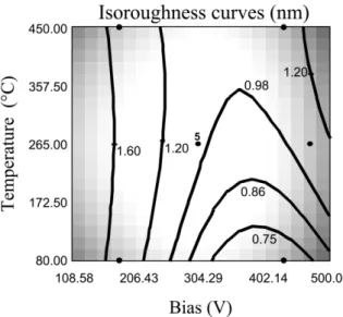
3.4. Roughness
Finally, the samples have been analysed by AFM. All the pictures are quite similar(Fig. 8). The RMS devia-tion are calculated from several pictures taken on each sample w10x. Here again, the results are treated by the
DESIGN-EXPERT䉸 software. With the theoretical
iso-roughness curves(Fig. 9), we can observe that the bias
voltage has a great influence on the roughness. An optimal bias appears at approximately y360 V. On the opposite, the roughness seems to be quite indifferent to the substrate temperature. The fact that the roughness is increasing after a critical value of bias voltage is explained as follows. The negative bias voltage of the
Fig. 8. AFM picture of ZrN film.
Fig. 9. Isoroughness curves obtained byDESIGN-EXPERT䉸.
substrate induces a bombardment of the growing film by the positive ions of the plasma. The collisions smooth the film surface and the roughness decreases. However, when the ions energy is too high, the film surface starts to be sputtered and the roughness increases again. 4. Conclusions
We have correlated the shapes and the positions of the XPS peaks with the stoichiometries of the ZrNx films thanks to the combination of XPS, RBS and NRA techniques. The positions of the N1s and Zr3d peaks
corresponding to the ZrN and ZrN stoichiometries have2 been defined.
The measurements of the roughness, resistivity and reflectivity of the ZrN films have pointed a substrate temperature and bias voltage limits. Over these limits, these three parameters deteriorate. We have observed that a substrate temperature of approximately 350 8C and a bias voltage of y350 V allows us to obtain a ZrN film with optimum features.
For industrial applications of these results, the opti-mum conditions in bias voltage and substrate tempera-ture must be adjusted to the real coating equipment and all coating conditions.
Acknowledgments
M. Del Re thanks the Fonds pour la Recherche dans l’Industrie et l’Agriculture (FRIA, Brussels) for finan-cial support.
References
w1x I. Bertoti, S.O. Saied, Surf. Interface Anal. 21(1994) 467–473. w2x L. Pichon, T. Girardeau, A. Straboni, F. Lignou, P. Guerin, J.´
Perriere, Appl. Surf. Sci. 150` (1999) 115–124.
w3x V. Vancoppenolle, P.-Y. Juan, M. Wautelet, M. Hecq, J. Vac.
Sci. Technol. A 17(6) (1999) 3317–3321.
w4x A. Tarniowy, R. Mania, M. Rekas, Thin Solid Films 311 (1997) 93–100.
w5x P. Prieto, L. Galan, J.M. Sanz, Surf. Interface Anal. 21(1994)
395–399.
w6x J.M. Sanz, L. Soriano, P. Prieto, G. Tyuliev, C. Morant, E.
w7x G. Terwagne, J. Colaux, G.A. Collins, F. Bodart, Thin Solid
Films 377–378(2000) 441–446.
w8x Optimisation des conditions operatoires de la spectrometrie de´ ´ masse des decharges electriques magnetrons par la methodol-´ ´ ´ ´ ogie des plans d’experiences Sabine Springael, Memoire de´ ´ Licence en Sciences Chimiques, 1994.
w9x Charles Kittel, Physique de l’etat solide, Editions DUNOD,´ 301.
w10x Pascal Viville, Analyse par Microscopie a force atomique de` biomateriaux polymeres a surface heterogene Ph.D. Thesis,´ ` ` ´ ´ ` UMH, 1997.