RESEARCH OUTPUTS / RÉSULTATS DE RECHERCHE
Author(s) - Auteur(s) :
Publication date - Date de publication :
Permanent link - Permalien :
Rights / License - Licence de droit d’auteur :
Bibliothèque Universitaire Moretus Plantin
Institutional Repository - Research Portal
Dépôt Institutionnel - Portail de la Recherche
researchportal.unamur.be
University of Namur
Ultralocal modification of surface plasmons properties in silver nanocubes
Mazzucco, S.; Stéphan, O.; Kociak, M.; Geuquet, N.; Henrard, L.; Ye, J.; Van Roy, W.; Van
Dorpe, P.
Published in: Nano Letters DOI: 10.1021/nl2037672 Publication date: 2012 Document VersionPublisher's PDF, also known as Version of record Link to publication
Citation for pulished version (HARVARD):
Mazzucco, S, Stéphan, O, Kociak, M, Geuquet, N, Henrard, L, Ye, J, Van Roy, W & Van Dorpe, P 2012, 'Ultralocal modification of surface plasmons properties in silver nanocubes', Nano Letters, vol. 12, no. 3, pp. 1288-1294. https://doi.org/10.1021/nl2037672
General rights
Copyright and moral rights for the publications made accessible in the public portal are retained by the authors and/or other copyright owners and it is a condition of accessing publications that users recognise and abide by the legal requirements associated with these rights. • Users may download and print one copy of any publication from the public portal for the purpose of private study or research. • You may not further distribute the material or use it for any profit-making activity or commercial gain
• You may freely distribute the URL identifying the publication in the public portal ?
Take down policy
If you believe that this document breaches copyright please contact us providing details, and we will remove access to the work immediately and investigate your claim.
Ultralocal Modification of Surface Plasmons Properties in Silver
Nanocubes
Stefano Mazzucco,
†Nicolas Geuquet,
‡Jian Ye,
§Odile Ste
́phan,
†Willem Van Roy,
§Pol Van Dorpe,
§Luc Henrard,
‡and Mathieu Kociak*
,††Laboratoire de Physique des Solides, University Paris-Sud, CNRS, UMR 8502, F-91405 Orsay Cedex, France ‡Department of Physics, University of Namur (FUNDP), 61 Rue de Bruxelles, 5000 Namur, Belgium §Imec vzw, Kapeldreef 75, B-3001, Leuven, Belgium
ABSTRACT: The plasmonic properties of individual subwavelength-sized silver nanocubes are mapped with nano-metric spatial resolution by means of electron energy-loss spec-troscopy in a scanning transmission electron microscope. Three main features with different energies and spatial behavior (two peaked at the corners, one on the edges) are identified and re-lated to previous measurements on ensemble or individual nanoparticles. The highly subwavelength mapping of the energy
position and intensity of the excitations shows that the surface plasmon modes, localized at specific areas of the particles, for example, the corners or the edges, are modified by their size, the presence of a substrate, and the very local environment. Helped by discrete dipole approximation numerical simulations, we discuss how local modifications of the environment affect the global modes of the particles. In particular, we show both experimentally and theoretically that absorption resonances at different corners of the same nanocube are largely independent of each other in energy and intensity. Our findings provide a better understanding of the spatial coherence of the surface plasmons in nanoparticles but also give useful insights about their roles in the nanoparticle sensing properties.
KEYWORDS: Surface plasmons, nanoparticles, nanocubes, electron energy loss spectroscopy (EELS), discrete dipole approximation (DDA), spatial coherence
I
t has been extensively reported that a deep understanding of the physical properties lying beneath the localized surface plasmons (LSPs) in metallic nanoparticles (NP) could open the path to extremely useful applications ranging from medicine to electronics. The study of LSPs at the sub-NP level has been recently shown to be possible with various techniques, includ-ing scanninclud-ing near optical microscopy (SNOM),1photon elec-tron emission microscopy (PEEM),2cathodoluminescence (CL),3 electron energy loss spectroscopy (EELS),4,5and photochemical imaging.6 In particular, having a spatial resolution of a few nanometers, EELS in a scanning transmission electron micro-scope (STEM) is a very effective technique in the study of LSPs in metallic nanoparticles (e.g., individual silver triangular prisms,4,7 gold nanorods and nanospheres,5,8,9 nanostars10) and more complex lithographied structures.11−13Most of the applications rely on the fact that the electro-magnetic field induced by LSP excitations is confined at the vicinity of the nanoparticle and is locally enhanced at specific positions on the NP’s surface.14Such local enhancement makes possible, for example, the acquisition of surface enhanced raman scattering (SERS) signal on single molecules, which could not be possible otherwise.10In textbook cases, the surface plasmons are considered to be spatially coherent over the whole extent of subwavelength-sized NPs. For example, a 10 nm diameter metal sphere exhibits a dipolar mode with field enhancement at both poles. A local modification of the environment (e.g., the sphere
is lying on a surface) would have a global effect on the energy and symmetry of the LSP modes. An important consequence is that, although the fields can be localized over distances smaller than the typical wavelengths in the vacuum, the excitation is coherent on the whole NP. Such coherence of LSP is also obtained when one spatial dimension of the particle is smaller than the skin depth of the metal, as shown for nanoantennas15 or nanoplatelets.16In these cases, strong and localized coherent enhancement can be observed on different areas of the nano-objects, even when separated by distances much larger than the skin depth mediated by plasmonic standing waves.16Also, as the size of the object becomes larger than the typical vacuum wavelength, coherence is recovered for surface plasmon polaritons.
In this paper, we explore the conditions to have spatially coherent LSPs or not over a metallic nanoparticle. The sensing properties of metallic NPs depend on the global NP response to a change of environment that, in turn, could be local. We investigate such effects for a system, silver nanocubes, with a rather complex LSP excitation scheme and modes localized at its corners, edges, and faces. The local modification is investigated
Received: October 25, 2011 Revised: January 11, 2012 Published: January 20, 2012
for two cube sizes and through two substrates, onto which the NPs are deposited, and through the local deposition of amorphous material.
The STEM-EELS experiments described here make possible to access the whole spectral information (e.g., energy posi-tion and intensity of the excitaposi-tions) at the nanometer scale in the near-infrared-to-ultraviolet regime in combination with the parallel acquisition of images (high angle annular dark-field (HAADF) imaging). Discrete dipole approximation (DDA) simulations are used to support our conclusions.
Silver nanocubes are studied here as a playground to probe the effect of the substrate and of the local environment on the LSP optical properties, thanks to their high level of symmetry. On one hand, Fuchs17was the first to envision theoretically the response of a cubic particle described by a model dielectric constant in the electrostatic limit. In the case of ionic nano-cubes, several surface phonon modes coexisting in a relatively narrow energy range were predicted. These results remain formally valid for LSPs provided that a dielectric constant adapted to the optical response in the UV−visible range is considered.18On the other hand, the optical properties of Ag nanocube have been extensively measured19−21as well as their SERS properties revealed.22,23Within these studies, the effects of many parameters, that is, environment and substrate,19,24,25 shape of the corners,21cube orientation23and size,25have been investigated using either ensemble or individual nanocube measurements supported by numerical simulations. However, although the numerical simulations can predict the spatial distribution of the LSP modes within the particles, no experi-mental evidence has been reported, to the authors’ knowledge, due to insufficient maximum spatial resolution that can be achieved. Moreover, studies on the effects of local modifica-tions, that is, within few nanometers, on nanocubes seem to be scarce.
The silver nanocubes have been synthesized and charac-terized as explained by Ye et al.20For STEM-EELS, the NPs were deposited on a 25 nm thick Si3N4 membrane or on a
cleaved KAl2(AlSi3O10)(OH, F)2(mica) substrate. Si3N4has a gap at 5 eV, while mica has a gap at 6.5 eV.26,27This makes the two materials suitable for low energy-loss experiments in the energy range of the visible spectrum. Since the two substrates have a different refractive index, n = 2.05 for Si3N4and n = 1.56 for mica, the effect of the substrate on LSPs can also be inves-tigated. Aggregates of nanoparticles were observed on both Si3N4 and cleaved mica substrates with the majority of the
particles having a cubic shape with smooth corners. When indi-vidual cubes were found, the average edge size was about 60 nm with yet larger sizes available.
The chrono spectrum-image (ChSPIM) technique,4a modi-fication of the spectrum-image (SPIM) method,28 has been used to acquire the data: the electron probe of the STEM scans over the area of interest of the sample collecting 50 complete energy-loss spectra at each pixel. The dwell time is typically 3 ms for each spectrum, while the energy range falls in the visible spectrum (1.7 to 3.1 eV). For every experiment, the SPIMs have been calibrated using the well-known bulk plasmon mode of silver at 3.8 eV, resulting in an energy dispersion of about 0.045 eV/ch. The scanned area is typically subdivided into 32 × 32 pixels and, depending on the magnification, the spatial sampling goes from about 3 to about 9 nm per pixel. Along with the EELS spectra, a HAADF image is acquired. This allows one to compare directly the EELS signal with the morphology of the sample. Also, the ChSPIM method allows
one to maximize the signal-to-noise ratio (SNR) and partially eliminate the instabilities due to the mains frequency. This is critical in the study of LSPs because the resonances in the energy-loss spectrum fall very close to the elastic peak (ZLP). After the acquisition, the spectra corresponding to each pixel are aligned along the ZLP and summed, so that a conventional SPIM is recovered. Then, the Richardson−Lucy (RL) de-convolution29 is applied to the entire data set in order to decrease the full width at half-maximum (fwhm) of the ZLP and thus enhance the signal due to the LSPs. Typically, a 5 to 15 iterations deconvolution is applied to the data. However, in one exceptional case the deconvolution process has been pushed up to 200 iterations (see the nanocube presented in Figure 1) in
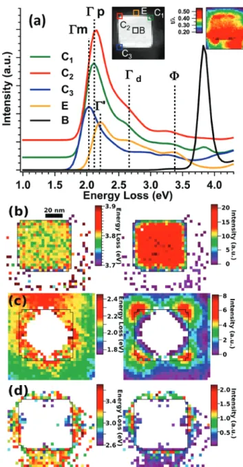
Figure 1.(a) Electron energy-loss spectra extracted from the SPIM of a 60 nm Ag cube on Si3N4substrate depicted in the HAADF image in the middle inset; right inset: thickness map expressed in unit of the electron mean free path, showing the deposit of material at the bottom of the cube. (b−d) Energy and intensity maps in the range of the bulk mode (b), theΓ and Γ′ modes (c) and the Φ mode (d). C1 and C2 spectra are vertically offset to improve the readability.
Nano Letters Letter
dx.doi.org/10.1021/nl2037672| Nano Lett. 2012, 12, 1288−1294 1289
order to verify that the results were consistent with the lower iteration analysis. Finally, the data set is treated with procedures developed in-house to subtract the ZLP and fit the detected peaks with Gaussians. The maps of the plasmon modes features (energy, intensity) can then be obtained (see ref 30 for details). The procedures are available upon request from the correspond-ing author. This method has been already successfully applied to the analysis of various plasmonic systems.4,16,12,31
Figure 1 shows the energy-loss spectra extracted from a SPIM of a 60 nm edge silver nanocube deposited on Si3N4and
the maps of the energy and intensity of the detected surface plasmon resonances. Electron energy-loss spectra summed over selected pixels (see inset) of the SPIM are shown in Figure 1a. The insets show the HAADF image and the relative thickness (in units of electron mean free path, t/λ) map of the nanocube. Spectrum B, acquired at the center of the particle, shows the well-known bulk plasmon of silver at 3.8 eV. In both spectra C1
and C2, acquired at the corners of the cube, a surface plasmon
resonance centered around 2.1 eV is detected, along with a shoulder around 2.65 eV; these modes will be calledΓpandΓd, respectively. When the probe moves toward the middle of the cube’s edge (E trajectory), two other surface plasmons arise at 2.2 eV (Γ′) and 3.3 eV (Φ). No relevant features have been measured when the probe was focuzed far from the nanocube. We stress here that in the geometry of the experiment the impinging electron is perpendicular to the substrate. As a con-sequence, the LSP modes for the C1, C2, and C3trajectories of the beam (see Figure 1) could have an electromagnetic response located both at corners (nearby and far from the substrate) and/ or at the vertical edge. Similarly, theΦ mode for the E trajectory actually probes the edge and the face of the cube.
The experimental energy and intensity maps of the bulk mode of silver are shown in Figure 1b. With the exception of some pixels outside the cube that have been incorrectly fitted, both the energy and intensity maps show how the peak at ∼3.8 eV is detected only inside the cube as expected. The energy distribution within the energy map of the bulk mode is centered at 3.796 eV with a fwhm of 0.016 eV; the relative precision is then 0.4%, demonstrating the reliability of the measurements and data analysis. Thanks to the high number of iterations in the RL deconvolution it has been possible to obtain an average width of 0.12 eV for this mode. The intensity map is also very interesting; the strength of the bulk mode is decreased by a factor of∼2 within one pixel (3.1 nm) of the cube’s surface. This is a direct observation of the renormaliza-tion of the bulk plasmons intensity due to the presence of the surface (Begrenzung effect).
Figure 1c (respectively d) shows the energy (left) and intensity (right) maps corresponding to the LSP modesΓ (respectively Φ) and presents an approximate 4-fold symmetry. However, the horizontal symmetry is slightly broken as seen for trajectory C3
(bottom left of the cube) for which an unique red-shifted mode Γmappears. TheΓdmode could not be mapped, although it is
present on averaged spectra on the upper side of the map (see also the C1, C2, and E trajectories). As a general tendency, the intensity ratio IΓp/IΓdbetween the modes is higher at the corner
than at the middle of the edge.
To help interpreting the experimental data, we performed DDA simulations for Ag nanocubes. Because the optical re-sponse of nanocubes is quite intricate, we first discuss the case of nanocubes in the vacuum to explore the expected size effects on both optical and EELS response, then we discuss the effect of the substrate based on simulations corresponding to the
situation investigated experimentally in Figure 1. The simulated optical (dashed lines) and EELS responses (solid lines) are displayed in Figure 2 for 10, 60, and 90 nm edge NPs
together with the spatial mode distributions. The optical spectra have been obtained with the DDSCAT code32and the EELS obtained with the homemade DDEELS code.33,34 The dielectric properties of Ag have been taken from ref 35 and 8000 dipoles have been used to discretize the cubes.
The smallest cube (10 nm) lies in the electrostatic limit (i.e., no retardation effects are expected) while the two larger ones have the sizes of the experimentally analyzed NPs (as displayed in Figures 1 and 4). The 10 nm edge cube shows a major opti-cal absorption, and no scattering, at around 3 eV and less intense features (3.2 and 3.4 eV), which is in agreement with previous works.19,25 We insist here on the complex LSP structure of metallic cubes that is observed when a model dielectric function with small damping is used.17,18,24When a tabulated dielectric function is considered, as it is the case here, numerical simula-tions show one or two broad peaks as seen in Figure 2 and in agreement with the experimental data.19,36 It has already been shown that the splitting of the two main resonances (such as the one for theΓ mode in Figure 2) may depend on either the cube size25or the interaction with a substrate.19In the latter case, the modes have been named distal and proximal by ref 36 and the interaction with the substrate explains the degeneracy lifting. For what concerns the size effect, theΓ peak has been shown to be the combination of a dipolar (D) and a quadrupolar (Q)
Figure 2.Optical and EELS DDA simulations for silver nanocubes in vacuum with various edge lengths. From top to bottom: 10, 60, and 90 nm. On each panel, the optical extinction, absorption and scattering (dashed lines), and EELS spectra for the C and E trajectories (solid lines) are displayed. The norm of the total electric field induced by a plane wave with an electric field pointing out of the picture and an horizontal wave vector are plotted for the three main modes,Γ, Γ′, and Φ (top of the figure).
mode that are degenerated in energy for small edge sizes. The modes then split at larger sizes due to retardation effects.24It is worth noting that both the dipolar and quadrupolar modes exhibit a charge distribution with an extremum at each of the eight corners of the cube. The main differences is the relative sign, or phase, of the charge density at each corner.24 In the case of the dipolar mode, if the sign of the charge density is positive at each corner of a given face, then it will be negative on the opposite side. In the case of the quadrupolar mode, the signs are alternating from one edge to the other around an axis passing through the center of a face. The quadupolar mode is shown here to be less intense optically for the considered size of NP. On Figure 2, we also see that the dipolar mode, mainly related to the scattering, rapidly shifts when the cube size increases and that the quadrupolar mode, mainly related to the absorption of light, is less dispersive.
The simulations of EELS spectra on the same Figure 2 show that an electron passing nearby the corner of a cube (C trajectory) excites preferentially the Q mode, even if the D mode is dominant in the optical spectra. As a consequence, the optical scattering spectrum and the EELS do not probe the same plasmon modes, especially as the size of the particle increases. We conclude here that theΓ mode that would be observed in EELS for a cube in the vacuum is directly related to the Q mode whereas the optical measurements probe both the Q and D mode, depending of the size and on the geometry of the experiments. However, at this stage, if only the Q mode is excited (at 2.9 eV for a 60 nm cube) by an electron trajectory passing near the corner of the cube (C), it cannot explain the presence of the three modes,Γd(2.65 eV),Γp(2.11 eV), andΓm(2.03 eV).
A Γ′ mode is also simulated for the optical absorption (Figure 2) with a spatial distribution centered on the corners of the cube, but less localized on the extreme tip of the cube. In simulated EELS spectra, it also appears for an intermediate electron trajectory (between C and E (not shown)). Note that an experimentalΓ′ mode having a similar spatial distribution is detected for an electron trajectory displaced from the corner such as the E trajectory in Figure 1. At the corner, however, the experimental Γ′ cannot be detected as it is embedded in the experimentalΓ mode, very close in energy and which is much stronger at the corners.
For an electron trajectory mimicking the E trajectory of the experiment, a resonance is obtained at 3.4 eV. Its spatial distribution can be identified with theΦ mode experimentally observed at 3.15 eV. In the simulation, a resonance at 3.7 eV is also observed but this seems not to correspond to any experi-mental feature. The origin of this discrepancy has to be analyzed in a future work.
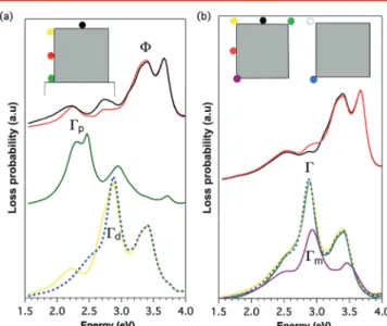
Now that we have clearly identified the feature of EELS experiments and compare them to optical measurements, the substrate effect can be taken into account. In optics, the pre-sence of a substrate leads to a splitting ofΓ modes.19,36,24On Figure 3a, we present EELS simulations for a 60 nm Ag nano-cube deposited on a Si3N4 substrate (n = 2.05) (solid lines),
compared with the one obtained for an isolated cube (dashed lines, same data than in Figure 2). The electron trajectories are taken parallel to the substrate for technical reasons (see ref 33 for details) and can be visualized on the figure (inset). Although this is not the same geometry as in EELS experiments, it still catches the influence of substrate on the LSP resonances. TheΓ mode is shifted to 2.14 eV when the electrons passes close to the corner of the cube in contact with the substrate (the electrons actually passes close to two corners, both in contact to the
substrate) (middle curve). For an electron trajectory exploring the Γ mode for a corner far from the substrate, (almost) no shift is observed (bottom curves).
Figure 3b displays the induced field of the modes as excited by the electron passing by the middle of an edge. We have chosen this particular trajectory because both modes are excited with a similar probability. It then allows a direct comparison between the mode maps. A clear similarity with the distal and proximal mode features described previously36suggests that the splitting of the mode observed for a corner trajectory is related to an interaction with the substrate. Finally, theΦ mode instead does not exhibit a noticeable shift due to the substrate.
With the support of the above simulations, we can now interpret unambiguously the experimental data displayed in Figure 1. TheΦ mode is clearly well reproduced by the simula-tions and will not be discussed further. We have seen experi-mentally that the Γ mode is split into two components Γp
andΓd at around 2.1 and 2.65 eV, respectively, and that the
simulations have predicted the distal and proximal modes at 2.1 and 2.9 eV. As previously stated the experimental trajectory passes by two corners, one close to the substrate, one far from it and then excites both modes. Having in mind the uncertainties on the exact shape of the cube (local deformations are possible), we can assign the two observed modes to the modes associated to the two local environments (with and without substrate), which is in fair agreement with the experimental results. We note that the distal mode has an energy almost equal to theΓ mode in the vacuum (see Figure 3), as expected. The simulation also agrees with the experimental finding that the intensity ratio IΓp/IΓdis higher at the corners than at the middle of the edge. The very low intensity of the Γp mode in the experimental
spectra cannot be explained at this stage. It is not related to the different electron trajectories (parallel and perpendicular to the substrate) as it will be shown in the following example. It can be related to a local modification of the shape of the corner of the cube (snipping) near the surface (that cannot be observed in STEM) or to a local contamination localized near the sub-strate (see below).
The experimental data of Figure 1c put in evidence a slight change in intensity between the mode situated at the top and at the bottom of the figure. However, the occurrence of theΓm mode and the vanishing of the Γp and Γd modes cannot be Figure 3.Substrate effect on a 60 nm Ag cube on Si3N4simulated by DDA. (a) EELS spectra for various trajectories for a cube lying on the substrate (solid lines) and isolated (dashed lines). Top: edge trajectory far from the substrate. Middle: corner trajectory close to the substrate. Bottom: corner trajectory far from the substrate. Inset: schematic view of the electron trajectory. (b) Map of the modulus of the induced electric field for the modes at 2.13 and 2.93 eV for an electron trajectory indicated by the white spot. Red, maximum; blue, zero.
Nano Letters Letter
dx.doi.org/10.1021/nl2037672| Nano Lett. 2012, 12, 1288−1294 1291
related to a substrate effect. Instead, it can be explained by an amorphous material contamination happening during the scan (starting from the top left of the figure, line by line). The accumulation of the amorphous material (seen on the HAADF images and the relative thickness measurements) modifies the local environment and thus the resonance behavior of the plasmon. Both corners share now the same environment, the amorphous contamination. Thus, theΓp andΓdmerge into a single mode that is red-shifted.
Considering now the second set of experimental data re-ported here, Figure 4 shows the energy-loss spectra, HAADF
image, relative thickness, LSP energy and intensity maps for a 90 nm edge silver nanocube lying on mica, a different substrate than in the previous example. In the energy-loss spectra, two peaks are detected at 3.1 and 2.6 eV when the electron beam passes close to the corners of the cube (spectrum C1). We also note a breaking of the 4-fold symmetry with a redshift and a merging of the modes associated with the spectrum C2(bottom
left corner of the cube). On the basis of their spatial distribu-tion, these three modes seem to derive from theΓ mode described
earlier. A resonance at 3.5 eV is detected at the edges of the cube (spectrum E) and is associated with the mode Φ pre-viously discussed. The energy and intensity maps for the LSP modes above corresponding to this mode are represented in Figure 4e.
Following the arguments developed for the 60 nm nano-cube on Si3N4, the two peaks at 2.6 and 3.1 eV can be directly
assigned to theΓpand Γd modes. The DDA simulations find such modes to have energies of 2.24 and 2.87 eV, respectively (Figure 5a). We note that, in this case, the intensity of the two
modes are similar in the simulation and in the experiment. As previously, theΦ mode does not exhibit a noticeable shift due to the substrate (black curve of simulated spectrum in Figure 5 compared with purple spectrum in Figure 2 (bottom)).
A closer view of theΓ modes is given in Figure 4d where the energy and intensity maps for the LSP modes below 3.1 eV are displayed. The redshift of the plasmon energy is clearly visible in the bottom left corner compared to the other three corners. At the same time, the relative thickness map (Figure 4c) shows that a contamination by amorphous material took place only in the bottom left area (a similar process that has been evoked for the cube of Figure 1). We can then directly correlate the presence of the local change of the LSP energy and intensity to a local change of the environment.
It has been impossible to discriminateΓpandΓdon
experi-mental maps due to a limitation of the automatic fitting proce-dure. As a result, the energy map in Figure 4d shows an averaged value of about 2.8 eV, however the two peaks appear well separated in the individual relevant spectra (spectrum C1). The
intensity map shows that the intensity of the plasmon modes is stronger at the corners, but it is locally damped in the con-taminated area.
It is interesting to note here that since the scan direction of the STEM probe is left−right top−bottom with respect to the
Figure 4.(a) Electron energy-loss spectra extracted from the SPIM of a 90 nm Ag cube on mica substrate for the trajectories indicated on the HAADF image (b). (c) Relative thickness map. (d,e) Energy (left) and intensity (right) maps for the C (corner) and E (edge) trajectories. The spectra are vertically offset to improve the readability.
Figure 5.Effect of the local environment on a 90 nm Ag cube on mica (n = 1.56) simulated by DDA. (a) EELS spectra for various trajectories for a cube lying on the substrate (solid lines) and isolated (dashed lines). Top: edge trajectories far from the substrate and close to it. Middle: corner trajectory close to the substrate. Bottom: corner trajectory far from the substrate (yellow). (b) Electron energy-loss spectra for a perfect isolated Ag nanocube (dashed line) and for a cube snipped on an edge (solid lines). The position of the electron beam with respect to the nanocube for each spectrum is given in the inset.
images, the contamination occurred in the bottom left corner before the bottom right corner was scanned. The plasmon energy of the bottom right corner is the same as the other non-contaminated corners. Hence, the contamination affected the corner mode on a local level leaving the other modes unaltered. This could be explained by the fact that the size of the studied cubes is larger than the skin depth of silver (∼20 nm at optical wavelengths).31This entails that the faces of the particles are not coupled, so that a LSP mode does not “see” the others contrary to what happens, for example, in thin silver triangular nanoprisms16or in nanoresonators.12
In order to have a better understanding of the experimental EELS data, we have performed DDA simulations of energy-loss spectra for a 90 nm edge cube in vacuum with and without a local environment modification. On Figure 5b, the dashed line presents the simulations for a perfect cube (identical to the curve in Figure 2 (bottom)). Instead, the solid line is relative to a cube with a snipped edge (see inset). The latter configuration has been chosen to simulate a very local change of the environ-ment of an edge of a cube when other edges are kept perfect. For the perfect cube, theΓ mode is obtained at 2.90 eV and theΦ mode at 3.40 eV. For the snipped cube, the resonance energies of theΓ and Φ modes remain unchanged, except for the spectrum corresponding to an electron trajectory passing very close to the defective edge; in such case the LSP is blue-shifted to 3.0 eV. A decrease in intensity is also associated to the fact that the electron probe is further from the cube and the blueshift is a known consequence of the snipping when all corners are modified.37,38 We emphasize here the very high localization of the effect: this simulation shows that a local change of environment leads to a change of energy of the Γ mode only for an electron trajectory passing nearby the modified edge, as observed experimentally. The very same effect appear with the nanocube of Figure 1 for which a contamination on both sides arose.
In conclusion, we have confirmed the existence of a local splitting of the corner (Γ) modes of nanocubes into a distal and proximal modes in presence of a substrate. Then, the localization of LSPs at the level of a single corner has been observed experimentally by EELS and has been confirmed by the DDA calculations. It has been shown how a very local change, in shape (snipping of one corner) or dielectric environ-ment (contamination, substrate), of the particle configuration alters the energy and intensity of the associated LSP mode. To the best of the authors' knowledge, this is the first time that the “locality” of the LSP modes is studied and that the decoupling of the resonances has been demonstrated. Finally, we want to point out the potential usefulness of the extreme locality of the Γ mode for sensing applications, where each individual corner, rather than a full nanoparticle, could be used as a plasmonic sensor.
■
AUTHOR INFORMATIONCorresponding Author
*E-mail: [email protected].
Notes
The authors declare no competing financial interest.
■
ACKNOWLEDGMENTSSimulations have been performed at the Interuniversity Scientific Computing Facility located at the University of Namur, Belgium, which is supported by the F.R.S.-FNRS under
convention No. 2.4617.07. The authors from Orsay and Namur acknowledge the WBI/FRS-FNRS/CNRS scientific coopera-tion program PHC “Tournesol”. The authors acknowledge financial support from the European Union (E4) under the Framework 6 program under a contract for an Integrated Infrastructure Initiative (reference 026019 ESTEEM). J.Y. and P.V.D. acknowledge financial support by the FWO-Flanders.
■
REFERENCES(1) Imura, K.; Okamoto, H. Bull. Chem. Soc. Jpn. 2008, 81, 659−675. (2) Douillard, L.; Charra, F.; Korczak, Z.; Bachelot, R.; Kostcheev, S.; Lerondel, G.; Adam, P. M.; Royer, P. Nano Lett. 2008, 8, 935−940.
(3) Gomez-Medina, R.; Yamamoto, N.; Nakano, M.; Abajo, F. J. G. New J. Phys. 2008, 10, 105009.
(4) Nelayah, J.; Kociak, M.; Stephan, O.; García de Abajo, F. J.; Tence, M.; Henrard, L.; Taverna, D.; Pastoriza-Santos, I.; Liz-Marzán, L. M.; Colliex, C. Nat. Phys. 2007, 3, 348−353.
(5) Bosman, M.; Keast, V. J.; Watanabe, M.; Maaroof, A. I.; Cortie, M. B. Nanotechnology 2007, 18, 165505.
(6) Hubert, C.; Bachelot, R.; Plain, J.; Kostcheev, S.; Lerondel, G.; Juan, M.; Royer, P.; Zou, S. L.; Schatz, G. C.; Wiederrecht, G. P.; Gray, S. K. J. Phys. Chem. C 2008, 112, 4111−4116.
(7) Nelayah, J.; Gu, J.; Sigle, W.; Koch, C. T.; Pastoriza-Santos, I.; Liz-Marzan, L. M.; van Aken, P. A. Opt. Lett. 2009, 34, 1003−1005.
(8) N’Gom, M.; Li, S. Z.; Schatz, G.; Erni, R.; Agarwal, A.; Kotov, N.; Norris, T. B. Phys. Rev. B 2009, 80, 113411.
(9) Chu, M.-W.; Myroshnychenko, V.; Chen, C. H.; Deng, J.-P.; Mou, C.-Y.; García de Abajo, F. J. Nano Lett. 2009, 9, 399−404.
(10) Rodriguez-Lorenzo, L.; Alvarez-Puebla, R. A.; Pastoriza-Santos, I.; Mazzucco, S.; Stephan, O.; Kociak, M.; Liz-Marzan, L. M.; de Abajo, F. J. G. J. Am. Chem. Soc. 2009, 131, 4616.
(11) Sigle, W.; Nelayah, J.; Koch, C. T.; van Aken, P. A. Opt. Lett. 2009, 34, 2150−2152.
(12) Boudarham, G.; Feth, N.; Myroshnychenko, V.; Linden, S.; Garca de Abajo, J.; Wegener, M.; Kociak, M. Phys. Rev. Lett. 2010, 105, 255501.
(13) Koh, A. L.; Fernandez-Dominguez, A. I.; McComb, D. W.; Maier, S. A.; Yang, J. K. W. Nano Lett. 2011, 11, 1323−1330.
(14) Ye, J.; Chen, C.; Lagae, L.; Maes, G.; Borghs, G.; Van Dorpe, P. Phys. Chem. Chem. Phys. 2010, 12, 11222−11224.
(15) Novotny, L. Phys. Rev. Lett. 2007, 98, 266802.
(16) Nelayah, J.; Kociak, M.; Stephan, O.; Geuquet, N.; Henrard, L.; de Abajo, F. J. G.; Pastoriza-Santos, I.; Liz-Marzan, L. M.; Colliex, C. Nano Lett. 2010, 10, 902−907.
(17) Fuchs, R. Phys. Rev. B 1975, 11, 1732.
(18) Ruppin, R. Z. Phys. D: At., Mol. Clusters 1996, 36, 69−71. (19) Sherry, L.; Chang, S.-H.; Schatz, G.; VanDuyne, R.; Wiley, B.; Xia, Y. Nano Lett. 2005, 5, 2034−2038.
(20) Ye, J.; Chen, C.; Van Roy, W.; Van Dorpe, P.; Maes, G.; Borghs, G. Nanotechnology 2008, 19, 325702 (6pp).
(21) McMahon, J.; Wang, Y.; Sherry, L.; VanDuyne, R.; Marks, L.; Gray, S.; Schatz, G. J. Phys. Chem. C 2009, 113, 2731.
(22) Rycenga, M.; Kim, M.; Camargo, P.; Cobley, C.; Li, Z.-Y.; Xia, Y. J. Phys. Chem. A 2009, 113, 3932.
(23) McLellan, J. M.; Li, Z. Y.; Siekkinen, A. R.; Xia, Y. N. Nano Lett. 2007, 7, 1013−1017.
(24) Zhang, S.; Bao, K.; Halas, N. J.; Xu, H.; Norlander, P. Nano Lett. 2011, 11, 1657−1663.
(25) Zhou, F.; Li, Z. Y.; Liu, Y.; Xia, Y. N. J. Phys. Chem. C 2008, 112, 20233−20240.
(26) Atkins, A. J.; Misell, D. L. J. Phys. C: Solid State Phys. 1972, 5, 3153−3160.
(27) Buechner, U. J. Phy. C: Solid State Phys. 1975, 8, 2781−2787. (28) Jeanguillaume, C.; Colliex, C. Ultramicroscopy 1989, 28, 252− 257.
(29) Gloter, A.; Douiri, A.; Tence, M.; Colliex, C. Ultramicroscopy 2003, 96, 385−400.
Nano Letters Letter
dx.doi.org/10.1021/nl2037672| Nano Lett. 2012, 12, 1288−1294 1293
(30) Zagonel, L. F.; Mazzucco, S.; Tencé, M.; March, K.; Bernard, R.; Laslier, B.; Jacopin, G.; Tchernycheva, M.; Rigutti, L.; Julien, F. H.; Songmuang, R.; Kociak, M. Nano Lett. 2011, 11, 568−573.
(31) Mazzucco, S.; Stephan, O.; Colliex, C.; Pastoriza-Santos, I.; Liz-Marzan, L. M.; de Abajo, J. G.; Kociak, M. Eur. Phys. J.: Appl. Phys. 2011, 54, 33512.
(32) Draine, B. T.; Flatau, P. J. J. Opt. Soc. Am. A 1994, 11, 1491− 1499.
(33) Geuquet, N.; Henrard, L. Ultramicroscopy 2010, 110, 1075. (34) Henrard, L.; Geuquet, N. DDEELS, version 1.07alpha; University of Namur: Namur, Belgium; http://perso.fundp.ac.be/∼geuquetn/ddeels.php. (35) Palik, E. D. Handbook Of Optical-Constants; Academic Press: New York, 1984; Vol. 1.
(36) Ringe, E.; McMahon, J.; McMahon, J.; Sohn, K.; Cobley, C.; Xia, Y.; Huang, J.; Schatz, G.; Marks, L.; VanDuyne, R. J. Phys. Chem. C 2010, 114, 12511.
(37) Kelly, K. L.; Coronado, E.; Zhao, L. L.; Schatz, G. C. J. Phys. Chem. B 2003, 107, 668−677.
(38) McLellan, J. M.; Siekkinen, A.; Chen, J. Y.; Xia, Y. N. Chem. Phys. Lett. 2006, 427, 122−126.