RESEARCH OUTPUTS / RÉSULTATS DE RECHERCHE
Author(s) - Auteur(s) :
Publication date - Date de publication :
Permanent link - Permalien :
Rights / License - Licence de droit d’auteur :
Institutional Repository - Research Portal
Dépôt Institutionnel - Portail de la Recherche
researchportal.unamur.be
University of Namur
Electronic dynamics in graphene and MoS2 systems
Mark, Géza; Fejér, Gyöngyi R. ; Vancso, Peter; Lambin, Philippe; Biró, László P.
Published in:Physica Status Solidi (B) Basic Research
DOI:
10.1002/pssb.201700179
Publication date:
2017
Link to publication
Citation for pulished version (HARVARD):
Mark, G, Fejér, GR, Vancso, P, Lambin, P & Biró, LP 2017, 'Electronic dynamics in graphene and MoS2 systems', Physica Status Solidi (B) Basic Research, vol. 254, no. 11, 1700179.
https://doi.org/10.1002/pssb.201700179
General rights
Copyright and moral rights for the publications made accessible in the public portal are retained by the authors and/or other copyright owners and it is a condition of accessing publications that users recognise and abide by the legal requirements associated with these rights. • Users may download and print one copy of any publication from the public portal for the purpose of private study or research. • You may not further distribute the material or use it for any profit-making activity or commercial gain
• You may freely distribute the URL identifying the publication in the public portal ?
Take down policy
If you believe that this document breaches copyright please contact us providing details, and we will remove access to the work immediately and investigate your claim.
Physica Status Solidi B (2017) DOI: 10.1002/pssb.201700179
Electronic dynamics in graphene and MoS
2
systems
Géza I. Márk *,1, Gyöngyi R. Fejér1, Péter Vancsó1,2, Philippe Lambin2, and László P. Biró1
1 Institute of Technical Physics and Materials Science, Centre for Energy Research, P.O Box 49, H-1525 Budapest, Hungary 2 Physics of Matter and Radiation, University of Namur, 61. Rue de Bruxelles, B-5000 Namur, Belgium
Keywords wave packet dynamics, band structure, defects in 2D materials, Scanning Tunneling Microscopy
We performed wave packet dynamical calculations for graphene- and MoS2 monolayers by a new formulation of the split-operator FFT method utilizing ab-initio band structure results into the kinetic energy operator. While the time dependent dynamics is available through the solution of the time dependent Schrödinger equation in wave packet dynamics, the energy dependent dynamics is calcu-lated by the application of the time-energy Fourier
trans-form to the wave function. Time dependent probability re-sults show an anisotropic spreading of the probability den-sity current. The magnitude and angular dependence of the anisotropy is dependent i) on the process creating the ini-tial wave packet (e.g. injection from an STM tip or scat-tering on an impurity) and ii) on the details of the band structure.
.
1 Introduction One of the possible material families of the post-Silicon era is the family of the two dimensional (2D) materials. Whereas graphene was the first member of this group, transition-metal dicalchogenides (TMDCs) pro-vide a large variety of properties [1,2], In order to analyse measurement results and to design nanoelectronic devices, it is important to precisely understand the dynamics of elec-trons in these materials. Wave packet dynamics (WPD) [3] is a flexible method to simulate electronic dynamics and transport phenomena at the nanoscale which is capable of calculating realistic models containing several hundred at-oms already on a personal computer. Given a Hamiltonian and an initial wave function, WPD yields the time depend-ent wave function by the solving of the time dependdepend-ent Schrödinger equation. By application of time-energy Fou-rier transform, the energy dependent dynamics is also avail-able. During the past two decades [4], we have been per-forming WPD calculations for many sp2 Carbon nanosys-tems. In all these calculations the physical system was mod-elled by some kind of
V
(r
)
potential function. In the first approximation [5,6] this potential function was a simple jel-lium potential. This was suitable to model the geometric ef-fects in Scanning Tunneling Microscopy (STM) imaging of carbon nanotubes (CNTs) [5,6].STM offers the possibility to study both the atomic and electronic structure of the same nanostructure with sub-na-nometer resolution. This unique advantage of the method is
* Corresponding author: e-mail [email protected], Phone: +36 1 392 2222, Fax: +36 1 392 2226, www.nanotechnology.hu
also its greatest difficulty: the influence of the geometry and the electronic structure is always intimately mingled in STM images and Scanning Tunneling Spectroscopy (STS) curves. In order to include electronic structure into the WPD calcu-lation, we began using a local atomic pseudopotential [7] modelling the π electron bands of the sp2 carbon sheet. This potential has two major advantages: i) it brings the specific electronic dynamics (linear dispersion near the K points for electrons near the Fermi energy (EF), trigonal warping for hot electrons, etc) of the π bands into the WPD calculation and ii) makes it possible to handle localized defects. We uti-lized this potential for many calculations, networks of CNTs [8], modelling tip induced anisotropic electron dynamics during the STM imaging of graphene [9], and scattering of electrons by grain boundaries in graphene [10,11].
Atomic pseudopotential WPD, though an effective and capable method, is limited by the availability of a suitable local atomic pseudopotential function, which is not readily available for every material systems. The Hamiltonian, however, contains both a kinetic- and a potential energy op-erator,
H
=
K
+
V
and modifyingK
provides us an addi-tional degree of freedom in describing electronic dynamics. In our pseudopotential Schrödinger WPD calculations the kinetic energy was quadratic ink
and the peculiarities of the graphene band structure (linear near K point, etc) was2 Márk, Fejér, Vancsó, Lambin, and Biró: Electronic Dynamics in Graphene and MoS2 Systems
introduced into the Hamiltonian by the
V
(r
)
potential function. Dirac equation WPD calculations [12], however, utilize a kinetic energy linear ink
, hence these calculations correctly reproduce the small excitation energy (linear) band structure of graphene without any potential term. By addi-tion of potential, and vector potential terms, Dirac equaaddi-tion WPD calculations can nicely reproduce a large variety of effects important in graphene, such as charge puddles [13] and magnetic phenomena [14].Possibilities of exploitation of the kinetic energy opera-tor does not end by using a quadratic or linear
k
depend-ence. TheE
=
E
n(k
)
dispersion relation contains the full electronic structure information for a given crystalline ma-terial and the dispersion relation is readily available from state-of-the-art band structure calculations for practically any material. In this paper we present a general method to include the band structure information into the WPD calcu-lation. First we demonstrate the method for the case of a graphene sheet, modelled by the simplest tight-binding band structure, then apply the method to analyse electronic dy-namics on monolayer MoS2 utilizing state of the art ab-initio results.The present calculations are aimed at illustrating the spreading of a localized WP in the context of transport. These do not intend to explore the relaxation of hot electrons prepared e.g. by optical excitations [15]. Localized WPs can be injected, for example, onto a 2D sheet by an STM tip. Zero temperature calculations exclude electron scattering by phonons. Bloch equation calculations [15,16,17], however, should be more appropriate to deal with phonons at finite temperature then time dependent Schrödinger equation.
Elastic collisions by impurities like Oxygen and other defects could be included by introducing appropriate scat-tering potentials in the Hamiltonian [13]. This will be done in a future step. The present paper can be considered as a preparatory stage for more realistic calculations.
The organization of the paper is as follows. Section 2 gives an outline of the WPD method and of the dispersion relations used for graphene and MoS2. In Sec. 3 numerical results are presented for spreading of the WPs on graphene and MoS2. Section 4 is devoted to the discussion of the re-sults.
Hartree atomic units are used in all formulas except where explicit units are given. SI units are used, however, in all the figures and numerical data.
2 Calculation methods
2.1 The split-operator FFT method In this method the time development of the
ψ
( t
r
,
)
wave function is computed from the time-dependent 3D Schrödinger equa-tion using the split operator Fourier-transform method [18]
)
,
(
)
,
(
r
t
t
e
iHˆ tψ
r
t
ψ
+
∆
=
− ∆)
(
3 2 / ˆ ˆ 2 / ˆ ) ˆ ˆ (t
O
e
e
e
e
−i K+V ∆t≅
−iK∆t −iV∆t −iK∆t+
∆
where the potential energy propagator is a simple multi-plication with
exp(
−
iV
(
r
)
∆
t
)
for local potentials, and the effect of the kinetic energy propagator)
2
/
ˆ
exp(
−
i
K
∆
t
is dealt with in k space by multiplicat-ing the momentum space wave function by2
exp(
−
i k
|
|
∆
t
/ 4)
. We are able to obtain all measura-ble quantities from theψ
( t
r
,
)
time dependent wave func-tion, such as the probability densityρ
( t
r
,
)
, the probabil-ity currentj
( t
r
,
)
, etc. By applying a t-E Fourier trans-form the (more conventional)ψ
( E
r
,
)
wave function and energy-dependent measurables are also available. One of the advantages of the split operator method is the norm con-servation of the WP, which is necessary to calculate accu-rate transport values during the simulation time.The
2
k
term in the kinetic energy expression is noth-ing else but the free spaceE
=
k
2/
2
dispersion relation of an electron. Indeed, the split operator method exactly re-produces the free-space evolution of the electronic wave packet for the case ofV
(
r
)
≡
0
zero potential. Why not changing the dispersion relation to anyE
=
E
n(k
)
func-tion, which correctly describes the electronic structure of the specific material? This can be done, indeed, and this makes it possible to go beyond the Dirac-like physics of graphene and to study such effects in WPD as trigonal warping and anisotropic spreading.2.2 Calculation of the dispersion relations We demonstrate the method in two examples: i) tight-binding (TB) description of graphene and ii) Density Functional (DFT) treatment of Molybdenum-disulphide (MoS2).
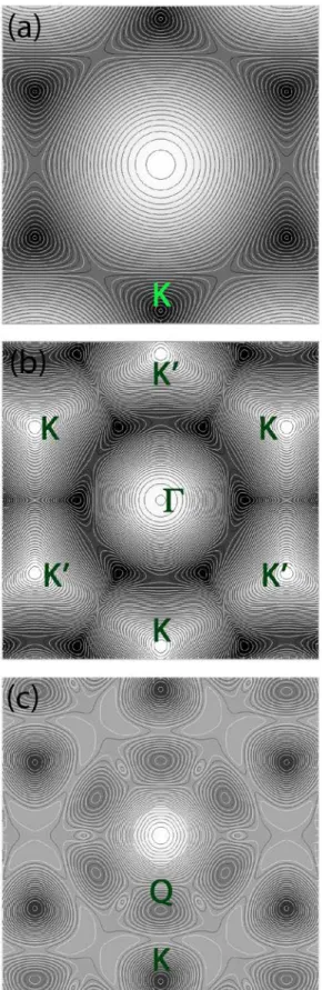
For our graphene calculations we used the simplest pos-sible TB approximation [19], with its six double Dirac cones at the six K points, as seen on Fig. 1a.
For the case of monolayer MoS2 a more sophisticated DFT calculations were performed using the Vienna ab initio simulation package (VASP) [20]. In DFT calculations the results depend on the approximation of the exchange corre-lation potential that describes the many-body interaction be-tween electrons. In the present paper we used the general gradient approximation (GGA) in the scheme of PBE (Perdew-Burke-Ernzerhof) functional [21]. Previous
calcu-1 2 3 4 5 6 7 8 9 10 11 12 13 14 15 16 17 18 19 20 21 22 23 24 25 26 27 28 29 30 31 32 33 34 35 36 37 38 39 40 41 42 43 44 45 46 47 48 49 50 51 52 53 54 55 56 57
lations show [22,23], that this functional gives proper de-scription of the MoS2 including the indirect-direct band gap transition when the bulk material is thinned to a monolayer, in good agreement with experimental findings [24].
In the calculation we used projector augmented wave (PAW) pseudo-potentials [25] and the kinetic energy cut-off for the plane wave expansion was 500 eV. The Brillouin-zone was sampled using with 8×8×1 Monkhorst−Pack mesh [26]. Figure 1b-c shows the calculated dispersion relations of the valence- and conduction bands. In order to focus on basic effects of the anisotropic WP spreading we neglected spin-orbit coupling – we will switch it back in a subsequent work.
3 Results In this section we analyse the time develop-ment of the direct space probability density function
)
;
,
(
x
y
t
ρ
. The momentum space probability density func-tionρ
(
k
x,
k
y;
t
)
remains constant, equal to its initial value,)
;
,
(
)
;
,
(
k
xk
yt
ρ
k
xk
yt
0ρ
=
. This is because the potential is zero in this calculation,V
(
r
)
≡
0
.All of our initial WPs studied in this paper are localized to a small spatial region in the direct space. The initial
)
;
,
(
x
y
t
0ρ
direct space probability density is a simple Gaussian for all the cases, but the complex phase of the wave function is a different function of the position in the different cases (K, K’, Q, Γ points), which corresponds to different initial momentum space wave functions, dictated by the analytic properties of the Fourier transform.Figure 2 shows the time development of the
ρ
(
x
,
y
;
t
)
probability density of the WP on graphene, when the initial state is a Gaussian located at one of the K points, i.e. the initial momentum-space wave function is2 2 ) (
)
0
,
(
x k kKNe
t
k
−∆ −=
=
ψ
, where N is a normaliza-tion constant and∆
x
is the direct space width of the Gauss-ian. The corresponding momentum space width of the Gaussian is∆
k
=
(
1
/
2
)(
1
/
∆
x
)
. The spreading of the WP shows an anisotropic time development, it splits into three parts, each moving away from the centre, showing a three-fold symmetry. This is because of the trigonal warping ef-fect around the K point (cf Fig. 1a).Figure 1
E
(
k
x,
k
y)
dispersion relation for graphene (tight-binding model) and MoS2 (DFT PBE calculation). (a) graphene4 Márk, Fejér, Vancsó, Lambin, and Biró: Electronic Dynamics in Graphene and MoS2 Systems
conduction band,
E
∈
[ ]
0
,
9
eV
(b) MoS2 valence band[
]
eV
E
∈
−
1
.
06
,
−
0
.
10
, (c) MoS2 conduction band[
]
eV
E
∈
1
.
58
,
2
.
70
. Black corresponds to energy minimum and white to energy maximum of the bands. There are 80 evenly spaced isoenergy contour lines in each figure. Those points of the Brillouin zone, which were used as wave packet starting points are marked with letters. (See the text for details.)Figure 2 Time development of the direct space probability density
of the wave packet on the graphene sheet. The momentum space wave function (not shown) is a Gaussian centred on the K point (marked in Fig.1a). White corresponds to zero probability and black to the maximum probability. Each snapshot is individually normalized. Size of the presentation window is 11.52 nm. Width of the initial Gaussian is
∆
x
=
0
.
187
nm
.The magnitude of the anisotropy depends on the
∆
x
parameter. A large
∆
x
(i.e. a small∆
k
) corresponds to a thin WP in momentum space, which means that the majority of the WP resides in the linear dispersion range around the K point, hence the WP evolution shows only negligible an-isotropy. A small∆
x
(i.e. a large∆
k
) represents, by con-trast, a wide dispersion in momentum space, the majority of the WP falls outside the linear dispersion range and that yields a considerable anisotropy in the time development. Indeed, the first two terms of the Taylor series expansion of the graphene TB dispersion relation around the K point isϕ
π
3
sin
2
2k
k
+
∆
∆
, which shows that the larger∆
k
is, the larger the three fold symmetric term becomes.The case of the MoS2 monolayer is more complicated. In this direct gap semiconductor there is a hole conduction at the six K points of the valence band, but the Γ point of the valence band is very close in energy to the K points. The lowest energy points of the first conduction band are also at the K points, but the Q points (halfway between Γ and K) are close in energy to the K points.
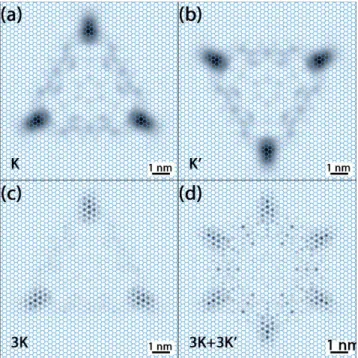
Figure 3 shows the
ρ
(
x
,
y
;
t
)
snapshots at t=14.5 fs at four characteristic initial WP positions at the MoS2 Brillouin zone for the valence- and conduction bands. The momentum space width of the initial WP was the same for all these four calculations (but larger as the value used for graphene, cf. Fig.2). When the initial WP is centred in the momentumspace at the K point, we see trigonal warping both at the valence- and conduction bands (Figs. 3a and 3c), though the valence band case shows a higher amount of anisotropy. This can be understood by looking at the dispersion relations shown on Fig.1, where the trigonal warping is considerably higher around the K points of the valence band (Fig.1b) than at the conduction band (Fig.1c). Figure 3b shows the t=14.5 fs probability density snapshot when the initial WP is cen-tred at the Γ point of the valence band. We see a slow iso-tropic spreading here, which can be explained by the slow and isotropic variation of the energy around the valence Γ point, cf. Fig.1b. Isoenergy contours around the Q point of the conduction band (halfway between Γ and K, cf. Fig. 1c) shows a peculiar distorted twofold symmetric pattern. This is the cause of the probability density pattern seen on Fig.3d.
Figure 3 MoS2 direct space probability density snapshots (t=14.5 fs) for different scenarios. (a) K point at the valence band (cf Fig.1b), (b) Γ point at the valence band (cf Fig.1b), (c) K point at the first conduction band (cf Fig.1c), (d) Q point at the first con-duction band (cf Fig.1c). White corresponds to zero probability and black to the maximum probability. Each snapshot is individually normalized. Size of the presentation window is 11.52 nm. Width of the initial Gaussian is
∆
x
=
0
.
374
nm
.Figure 4 shows
ρ
(
x
,
y
;
t
)
, the probability density of the direct space WP for t=14.5 fs for different initial wave packets for the case of the valence band. When 0(
k
)
ψ
is a Gaussian centred on one of the K points (Fig.4a), we see a trigonal warping effect similar to Fig.3a. This time, however, we choose a smaller direct space width for the Gaussian (thex
∆
parameter), which means a larger width in momentum space. This explains that the anisotropy is larger in Fig.4a1 2 3 4 5 6 7 8 9 10 11 12 13 14 15 16 17 18 19 20 21 22 23 24 25 26 27 28 29 30 31 32 33 34 35 36 37 38 39 40 41 42 43 44 45 46 47 48 49 50 51 52 53 54 55 56 57
than in Fig.3a. When the Gaussian is centred on a K’ point (Fig.4b), a similar pattern emerges, but rotated by 60o. The subsequent two images show situations, when the initial wave packet is a superposition of three Gaussians centred on the three K points (Fig.4c) and when it is a superposition of six Gaussians, centered on the three K and the three K’ points (Fig.4d). The three K points time development is very similar to that obtained for one K point, but a small wave-length, atomic scale modulation is seen on the probability density – similar to the HOMO-LUMO patterns calculated by DFT [27]. This is caused by interference of the plane wave parts of the three Gaussians in direct space. The three K – three K’ points case (Fig.4d) has a similar atomic scale modulation, but the envelope function shows a six-fold sym-metry in this case.
Figure 4 Direct space probability density snapshots (t=14.5 fs) for
different initial momentum space WP configurations in the MoS2 valence band, shown on Fig.1c. (a) Single Gaussian on a K point, (b) single Gaussian on a K’ point, (c) Superposition of 3 Gaussians at the 3 K points, (d) Superposition of 6 Gaussians at the 3 K and 3 K’ points. The atomic lattice is shown by thin lines. White cor-responds to zero probability and black to the maximum probability. Each snapshot is individually normalized. Size of the presentation window is 10.02 nm. Width of the initial Gaussian is
nm
x
=
0
.
187
∆
.4 Discussion Anisotropic WP spreading is seen for all the three studied dispersion relations: the graphene conduc-tion band, MoS2 valence- and conduction bands, but their magnitude is different. The width of the graphene conduc-tion band is nearly ten times as much as that of the MoS2 valence- and conduction bands (9 eV vs. 0.96 eV and 1.12
eV), hence the same initial direct space Gaussian width
∆
x
corresponds to a much larger energy distribution of the ini-tial WP for the graphene than for MoS2. Indeed, trigonal warping effects on graphene become apparent only for hot electrons having energy
E
F±
1
.
2
eV
but the energy rangeof the linear dispersion is only +-0.1 eV in MoS2. The shape of the dispersion relation around the K point is also different for the MoS2 valence- and conduction bands [28]: the isoen-ergy contours are much more distorted at the valence band which results a more pronounced anisotropy of the WP spreading for the case of the valence band, which affect transport in slightly p-doped configurations.
The specific form of the initial wave packet in a real sys-tem depends on how this initial state was created. In order to create a localized electronic state on the otherwise perfect 2D crystal lattice one needs some kind of localized pertur-bation. This localized perturbation can be, for example, an apex of an STM tip [9], or a structural defect [27]. As we showed earlier [9], the tunnelling from the STM tip to the graphene surface is a rather complex phenomenon and the details of this process determine, what will be the initial state of the further evolution of the WP on the graphene (or MoS2) sheet. The specific initial state is determined by many factors, e.g. the position of the tip and the bias voltage. These initial states correspond to the different initial mo-mentum space wave functions analysed in this paper.
Indeed, a localized WP can be created by inserting elec-trons from the STM tip into a slightly p-doped MoS2 sheet. As we have shown earlier for the case of graphene sheet [9], when the STM tip is above a center of a hexagon, the initial WP will have 6-fold symmetry, resulting a 6-fold symmetry in WP spreading (like in Fig. 4d), when it is above a carbon atom, the initial WP has 3-fold symmetry, causing a 3-fold symmetric spreading (like in Fig. 3c). If, however, the tip is placed to a point with no particular symmetry, e.g. displaced slightly from the “above the atom” position, this can lend a linear momentum to the WP specified by the direction of the above mentioned displacement. The linear momentum is represented in the direct space wave function as a plane wave component, which corresponds to a displacement of the wave function in momentum space. This way we can design “tailor made” initial WPs by carefully choosing the position of the STM tip.
In the case of slightly p-doped MoS2, transport will arise from few electrons around the K and K’ points of the first Brillouin zone. In the present non spin polarized calculation, K and K’ are perfectly equivalent, which means we have to deal with a symmetric combination of the 6 points (Fig.4d). In the presence of spin polarization, the valence bands around K and K’ points will be equally populated, but with electrons of opposite spins. For each spin, the current will spread like shown in Fig. 4c, but the total current will aver-age according to Fig. 4d.
Further localized perturbations may come from struc-tural defects, e.g. Sulphur vacancies, which cause mid-gap
6 Márk, Fejér, Vancsó, Lambin, and Biró: Electronic Dynamics in Graphene and MoS2 Systems
states in MoS2 [29]. These mid gap states have triangular and hexagonal atomic scale patterns observed recently in STM measurements [30]. Ghorbani et al analysed [27] the effect of different localized defects on the MoS2 transport for currents in the zigzag- and armchair directions, utilizing a non equilibrium Green function DFT approximation. Their results show a considerable anisotropy (difference of the zizag- and armchair current) for all studied localized de-fects.
5 Conclusions Investigating the anisotropy of the current in TMDC materials in the absence and presence of defects has a considerable importance. Our WPD calcula-tions based on ab-initio calculated energy dispersion rela-tions highlight an intrinsic anisotropy in the MoS2 band structure at low energies, which might give important infor-mation for future TMDC based nanoelectronic devices.
Acknowledgements This work was carried out within the
framework of the H2020 project 696656 Graphene Core1. GIM gratefully acknowledges support of the Belgian FNRS.
References
[1] Q. H. Wang, K. Kalantar-Zadeh, A. Kis, J. N. Coleman, and M. S. Strano, Nat. Nanotechnol. 7, 699 (2012).
[2] O. V. Yazyev and A. Kis, Mater. Today 18, 20 (2015). [3] B. M. Garraway andK.-A. Suominen, Rep. Prog. Phys. 58, 365
(1995).
[4] G. I. Márk, P. Vancsó, L. P. Biró, D. G. Kvashnin, L. A. Cher-nozatonskii, A. Chaves, Kh. Rakhimov, and Ph. Lambin, Wave packet dynamical calculations for carbon nanostruc-tures, Ser. NATO Science for Peace and Security Series B: Physics and Biophysics (Springer,Dordrecht,2016) , p. 89. [5] G. I. Márk, L. P. Biró, and J. Gyulai, Phys. Rev. B 58, 12645
(1998).
[6] G. I. Márk, L. P. Biró, and Ph. Lambin, Phys. Rev. B 70, 115423 (2004).
[7] A. Mayer, Carbon 42, 2057 (2004).
[8] D. G. Kvashnin, P. Vancsó, L. Y. Antipina, G. I. Márk, L. P. Biró, P. B. Sorokin, and L. A. Chernozatonskii, Nano Res. 8, 1250 (2015).
[9] G. I. Márk, P. Vancsó, C. Hwang, Ph. Lambin, and L. P. Biró, Phys. Rev. B 85, 125443 (2012).
[10] L. P. Biró and Ph. Lambin, New J. Phys. 15, 035024 (2013). [11] P. Vancsó, G. I. Márk, Ph. Lambin, A. Mayer, Y.-S. Kim, C.
Hwang, and L. P. Biró, Carbon 64, 101 (2013).
[12] K. S. Novoselov, A. K. Geim, S. V. Morozov, D. Jiang, M. I. Katsnelson, I. V. Grigorieva, S. V. Dubonos, and A. A. Firsov, Nature 438, 197 (2005).
[13] Kh. Yu. Rakhimov, A. Chaves, G. A. Farias, and F. M. Peeters, A. J. Phys.: Condens. Matter 23, 275801 (2011).
[14] V. Krueckl and T. Kramer, New J. Phys., 11, 093010 (2009). [15] S. Butscher, F. Milde, M. Hirtschulz, E. Malić, and A. Knorr,
Appl. Phys. Lett. 91, 203103 (2007).
[16] D. Brida, A. Tomadin, C. Manzoni, Y.J. Kim, A. Lombardo, S. Milana, R.R. Nair, K.S. Novoselov, A. C. Ferrari, G. Ce-rullo, and M. Polini, Nat. Commun. 4, 1987 doi: 10.1038/ncomms2987 (2013).
[17] Winzer T., Malić E., Knorr A., Graphene Bloch Equations. In: Egger R., Matrasulov D., Rakhimov K. (eds) Low-Dimen-sional Functional Materials. NATO Science for Peace and Security Series B: Physics and Biophysics. Springer, Dor-drecht (2013).
[18] M. D. Feit, J. A. Fleck, and Jr., A. Steiger, J. Comput. Phys.
47, 412 (1982).
[19] P. R. Wallace, Phys. Rev. 71, 622 (1947).
[20] G. Kresse and J. Hafner, Phys. Rev. B, 49, 14251 (1994). [21] J. P. Perdew, K. Burke, and M. Ernzerhof, Phys. Rev. Lett.
77, 3865-3868 (1996).
[22]A. Kuc, N. Zibouche, and T. Heine, Phys. Rev. B 83, 245213 (2011).
[23] H.-P. Komsa and A. V. Krasheninnikov, Phys. Rev. B 91, 125304 (2015).
[24] A. Splendiani, L. Sun, Y. Zhang, T. Li, J. Kim, Ch.-Yu. Chim, G. Galli and F. Wang, Nano Lett. 10 (4), 1271 (2010). [25] P.E. Blöchl, Phys. Rev. B 1994; 50, 17953 (1994).
[26] H. J. Monkhorst and J. D. Pack, Phys. Rev. B 13, 5188 (1976). [27] M. Ghorbani-Asl, A. N. Enyashin, A. Kuc, G. Seifert, and T.
Heine, Phys. Rev. B 88, 245440 (2013).
[28] A. Kormányos, V. Zólyomi, N. D. Drummond, P. Rakyta, G. Burkard, and V. I. Fal'ko, Phys. Rev. B 88, 045416 (2013). [29] J. Noh, H. Kim, and Y. Kim, Phys. Rev. B 89, 205417 (2014). [30] P. Vancso, G. Z. Magda, J. Peto, J. Y. Noh, Y. S. Kim, C. Hwang, and L. Tapaszto, Sci. Rep., http://doi.org/10.1038/srep29726.