HAL Id: hal-02111734
https://hal.archives-ouvertes.fr/hal-02111734
Submitted on 26 Apr 2019
HAL is a multi-disciplinary open access
archive for the deposit and dissemination of
sci-entific research documents, whether they are
pub-lished or not. The documents may come from
teaching and research institutions in France or
abroad, or from public or private research centers.
L’archive ouverte pluridisciplinaire HAL, est
destinée au dépôt et à la diffusion de documents
scientifiques de niveau recherche, publiés ou non,
émanant des établissements d’enseignement et de
recherche français ou étrangers, des laboratoires
publics ou privés.
Atomic redistribution of implanted Fe and associated
defects around moving SiO 2 /Si interfaces
Anthony de Luca, Nelly Burle, Alain Portavoce, Catherine Grosjean,
Stéphane Morata, Michael Texier
To cite this version:
Anthony de Luca, Nelly Burle, Alain Portavoce, Catherine Grosjean, Stéphane Morata, et al.. Atomic
redistribution of implanted Fe and associated defects around moving SiO 2 /Si interfaces. physica
status solidi (c), Wiley, 2015, 12 (8), pp.1166-1169. �10.1002/pssc.201400233�. �hal-02111734�
pss-Header will be provided by the publisher
Review copy – not for distribution (pss-logo will be inserted here
by the publisher)
Atomic redistribution of implanted Fe and
associated defects around moving SiO
2/Si
interfaces
Anthony De Luca1, Nelly Burle1*, Alain Portavoce1, Catherine Grosjean2, Stéphane Morata3, Michaël Texier1
1
Aix Marseille Université, CNRS, IM2NP UMR 7334, bd Escadrille Normandie Niémen F-13397 Marseille, France
2 ST Microelectronics, ZI Peynier Rousset F-13790 Peynier, France 3 Ion Beam Services, ZI Peynier Rousset F-13790 Peynier, France
Received ZZZ, revised ZZZ, accepted ZZZ
Published online ZZZ (Dates will be provided by the publisher.)
Keywords : TEM, diffusion, contamination, oxide.
The behaviour of Fe atoms at the Si/SiO2 interface, as a
modelisation of an involuntary Fe contamination before or during the oxidation process has been studied in Fe-implanted wafers. As-Fe-implanted and oxidized wafers were characterized by SIMS, APT, HR-TEM and STEM-HAADF. Successive steps of Fe segregation, iron-silicides precipitation and dissolution were identified. As expected for such a temperature range, the iron-silicide precipitates adopt the FeSi2 structure. Fe enriched phases
were also identified in an advanced step of precipitation. Dynamic mechanisms are proposed, taking into account the competitive oxidizing of precipitates and silicon ma-trix, to understand the different steps and precipitation phases observed in the samples during the non-equilibrium conditions due to the oxide layer growth. The correlation between the formation of characteristic py-ramidal defects at the SiO2/Si interface and the presence
of the Fe-rich precipitates is explained.
Copyright line will be provided by the publisher
1 Introduction Silicon oxide remains the main gate
oxide used in C-MOS technology. It still plays a key role in the advanced MOSFET technology as constituting a thin transition layer between the Si substrate and the high-k gate oxide layer [1]. However, metallic impurities in sili-con, even for low contamination levels, may affect hugely the reliability of the component by creating electric defects in the active region as well as by disturbing the quality of the interface SiO2/Si.
Iron is one of the most deleterious metallic contami-nants in silicon; various steps of the process can lead to Fe contamination via different sources (polishing slurries, im-purities in quartz tubes material, SiC boats, furnaces liners) [2], and because its high diffusivity [3] and capacity to act as donor [4] it is known to strongly degrade the device per-formances.
Fe contamination may affect the SiO2/Si interface
in-tegrity as it has been shown in various studies. For exam-ple, Honda et al., showed that -FeSi2 precipitates can
nu-cleate at the SiO2-Si interface, which is responsible for the
increase of leakage currents and leads to dielectric break-down in MOS capacitors [5]. SIMS measurements per-formed on Fe-contaminated, dry-oxidized Si wafers also evidenced iron atoms accumulation at the SiO2/Si interface
while a part of the iron atoms is trapped in the oxide layer [6]. Sadamitsu et al. identified the precipitation of the
cu-bic phase FeSi at the Si/SiO2 interface and identified
inclu-sions in the oxide as probably being Fe3O4 and -Fe2SiO4
precipitates [7]. Pyramidal defects and -FeSi2 precipitates
have been observed , with the same density, at the SiO2/Si
interface in surface Fe-contaminated Si wafers [8]. These authors suggested that the injection of excess self-interstitial Si atoms by FeSi2 precipitation would enhanced
the formation of such pyramids. Anyway, the alteration of electrical characteristics of devices would be due not only to the Fe-induced levels in the gap, but also to the reduc-tion of the grid oxide thickness [6]. It must be noticed that the size of the observed precipitates does not change with the contamination level and remains close to 10 nm in di-ameter. Similar pyramidal defects and precipitates were not observed in bulk-contaminated samples.
The aim of this work is to evidence the links between the two main defects in iron-contaminated wafers: precipi-tates and pyramidal defects, and to justify this correlation.
2 Materials and methods Fe implantation has been
performed in P doped (2-20 cm) (001) Si wafers (extrac-tion voltage of 65 kV, fluence of 1.0×10¹⁵ atomscm−2). The incidence angle of 7 ° from the Si(001) surface al-lowed reducing the channelling effect [9, 10].
2 Author, Author, and Author: Short title
Copyright line will be provided by the publisher
SIMS measurements were performed in as-implanted and oxidised samples until 500nm in depth. Fe-implantation profiles were also simulated by Stopping and Range of Ions in Matter (SRIM) calculations [11], taking into account the possible mixing artefact [12] , and by Atomic Probe Tomography (APT). These various tech-niques gave well correlated results; the concentration pro-files follow a gaussian distribution centred on a 55 nm-average implantation depth.
Oxidation of the implanted wafers was carried out by thermal annealing in oxygen atmosphere at 900 °C or 1100 °C for various durations. For this, the wafers were first introduced in a furnace at 800 °C under N2 flux.
Af-terward, the wafers were maintained under (N2)90%
+(O2)10% flux to avoid undesired nitriding of the surface
while the temperature was increased using a ramp of 5 °Cmin-1 until the annealing temperature (900 °C or 1100 °C) was reached. After being annealed under O2 flux,
the oxidized wafers were then cooled down to the room temperature under N2 atmosphere at 5 °Cmin-1. Oxide
layer thicknesses were determined using ellipsometry measurements.
Samples for transmission electron microscopy (TEM) and scanning transmission electron microscopy (STEM) analyses were prepared by focused ion beam (FIB) mi-cromachining using a FEI Helios 600 Nanolab microscope equipped with a Ga+ ion source.
TEM and STEM analyses were performed using a FEI Titan 80-300 Cs-corrected microscope operating at 300 kV
and equipped with annular HAADF-STEM detector. For both optimizing spatial resolution and reducing spatial de-localisation, spherical aberration Cs was adjusted to -7 µm
for TEM imaging.
3 Results and discussion
2.1 Fe implantation and precipitation SIMS
measurements and APT analyses revealed that the initial Fe distribution follows a gaussian profile with a maximum concentration at the depth of 55 nm. In as-implanted sam-ples, the presence of a superficial amorphous layer (thick-ness: 925 nm) was evidenced by TEM imaging.
However, the recrystalisation of this layer was ever complete in the sample annealed at 900 °C during 5 min, which is not surprising since the recrystallisation rate is es-timated to at least 1800 nmmn-1 at 800°C [14] so the whole 92 nm would be cured in less than 30 s . This fast recrystalisation leads to the formation of numerous end-of-range (EOR) defects [15] in the area corresponding to the initial interface between amorphous and crystalline silicon. However, no Fe segregation is evidenced on these defects, in contrast with the observation of Fe-decorated extended defects already reported in various studies [16--19]. In spite of the very short duration of the thermal annealing performed on this sample, post mortem TEM analysis also reveals the presence of precipitates at the SiO2/Si interface.
A rough estimation of 3108 precipitates per surface square centimetre is found. The observed precipitates exhibit fac-etted shapes, with facets parallel to the {114} and {111} atomic planes of the Si substrate. These precipitates reach in few cases a few tens of nanometres in diameter. It must be noticed that they are systematically totally included in the silicon substrate.
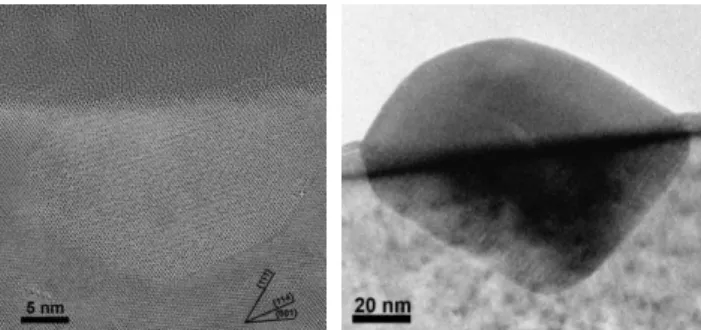
On the contrary, the precipitates observed in samples annealed for a longer time (i.e. 3h and 10h) usually strad-dle the interface between the substrate and the oxide layer. In that case, although the precipitates’ density and size (be-tween 20 nm and 50 nm) remain similar to the ones of the precipitates observed in the sample annealed during 5 min, their shape is slightly different. In particular, the part of the precipitates embedded in the oxide layer is rounded, that is in sharp contrast with the other part, faceted, contained in the silicon substrate (figure 1). This morphological change suggests that the precipitates were partially oxidized during the oxidation process of the silicon, leading to a vanishing of the faceting imposed by the symmetry of the surround-ing crystalline matrix when included in the silicon sub-strate, to the benefits of a more energetically favourable spherical shape in the amorphous oxide layer. The analysis of the Fourier transform of the HRTEM images systemati-cally confirms that the structure of these precipitates coin-cides with the -FeSi2 silicide.
Figure 1 Precipitates observed in Fe-implanted silicon
sub-strate (fluence: 1.0×1015 cm−2) and dry-oxidized at 900 °C during a) 5 min (left) and b) 10 hours (right).
2.2 Pyramidal defects at SiO2/Si interfaces and
correlation with precipitates Numerous pyramidal
de-fects, identified from HRTEM imaging as crystalline sili-con, were systematically observed at the SiO2/Si interface
in all samples. Their density and size are roughly about 2×108 cm-2, 10 nm × 30 nm in 900 °C samples, about 3×107 cm-2, 10-30 nm × 60 nm in 1100 °C samples (esti-mated from TEM observations).
Moreover, spherical -FeSi2 precipitates were
fre-quently observed at the top of pyramids (figure 2), that is supporting the hypothesis of a correlation between the presence of the precipitates and the formation of the pyra-mids. In the case of softer pyramids, smaller FeSi precipi-tates have also been identified, whereas their small size can
1 2 3 4 5 6 7 8 9 10 11 12 13 14 15 16 17 18 19 20 21 22 23 24 25 26 27 28 29 30 31 32 33 34 35 36 37 38 39 40 41 42 43 44 45 46 47 48 49 50 51 52 53 54 55 56 57
avoid them to be systematically detected. Finally, STEM-HAADF imaging revealed the presence of small Fe-rich clusters at the vicinity of pyramids in the oxide layer.
Considering the respective oxidation rates of silicon and iron-silicide precipitates, a faster oxidation rate of the
-FeSi2 precipitates in comparison with silicon would
sys-tematically lead to the observation of precipitates totally embedded in the silicon layer. On the contrary, the obser-vation of some of them partially or totally included in the oxide layer necessarily implies that bulk silicon is faster to oxidise than FeSi2 precipitates. Thus, natural explanation
of figure 2 is that the precipitate hinders the oxydation of silicon.
Figure 2 Example of pyramidal defect observed at the
SiO2/Si interface in oxidized silicon substrates previously
im-planted with Fe atoms, observed by HAADF-STEM imaging. Annealing conditions are 1100 °C, 12 min but similar configura-tions are observed in the others annealing condiconfigura-tions (except 900 °C, 5 min). The precipitate composition is FeSi2.
The advance of the SiO2/Si interface being locally
masked by the presence of a precipitate, a pyramid is formed below. Nevertheless, the lateral sides of pyramids are also oxidised, which progressively leads to the inclu-sion of the precipitate in the growing oxide layer. As far as the precipitate is totally included in the oxide, the pyramid is progressively consumed in the same time the interface is moving forwards. The shape evolution of pyramids would probably follow the sketch illustrated in figure 3.
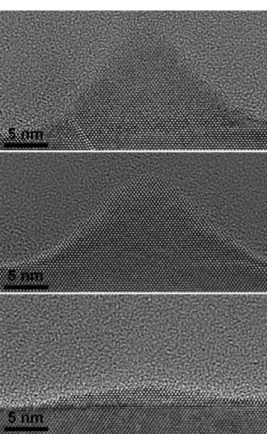
Some pyramidal defects are also observed whereas no precipitate is visible (figure 3). It could be attributed to natural roughness of the layer, but the most probable ex-planation is that the thinning of the sample can be located out of the medium plane of the pyramid so that the sample surface would be crossing the basis of the pyramid without intersecting the precipitate.
2.3 Diffusion of chemical species inside the precipitates Two main observations give evidence of
competition between the moving of interface and some dif-fusion mechanisms:
Figure 3 Various pyramidal defects observed at the SiO2/Si
interface in oxidized silicon substrates previously implanted with Fe atoms; Si pyramids are clearly coherent with the Si substrate. A stacking fault is visible within the pyramidal defect on the up-per image.
a) SIMS measurements reveal that the maximum con-centration of iron is always located at the interface, in good agreement with TEM observations in which big precipi-tates are consistently located in the vicinity of the SiO2/Si
interface whatever the oxidising time. So we can conclude that whereas the oxidation of Si is quicker than the oxida-tion of FeSi2, the precipitates move with the interface. It
implies both dissolution of the part of the precipitates in-cluded in the growing silicon oxide layer an the continu-ous growing of the FeSi2 phase at its interface with the
sili-con substrate; this is possible only if Fe atoms diffuse to-wards the substrate, whereas Si in FeSi2 is oxidized on the
top part;
b) In some cases, some other phases with higher Fe contents have also been observed, corresponding to ad-vanced oxydation phases (figure 4): a detailed analysis of these precipitates will be found elsewhere [20].
It is thus likely that diffusion of chemical species: Si and Fe, occurs inside the precipitates, and it can be as-sumed that several (Fe, Si) phases simultaneously co-exist, forming and vanishing in the same time in non-equilibrium conditions.
4 Author, Author, and Author: Short title
Copyright line will be provided by the publisher
5 nm
Figure 4 Nanometric FeSi precipitate at the top of a
pyra-mid (oxidation conditions 1100°C, 12 min).
2.4 Diffusion, precipitation and dissolution of Fe at the moving SiO2/Si interface The behaviour of implanted
iron during the oxidation annealing may then be described as follows:
a) Diffusion towards the surface occurs in 10-2 s, when the sample is introduced in the furnace at 800°C ;
b) in less than 5 min at 900 °C, the main part of iron is precipitated as facetted FeSi2 precipitates;
c) as the oxidation-front is moving forwards, precipi-tates follow the interface by Si oxidation–induced dissolu-tion on one side, and simultaneous -FeSi2 growth on the
other side;
d) -FeSi2 precipitates enriche in Fe because of
prefer-ential oxydation of Si atoms leading to the formation of Fe-rich phases for the longer times of oxidation;
e) nanometric Fe-rich clusters gettered in the SiO2
ox-yde layer remains observable in the vicinity of interfacial pyramids which would be the track of a dissolved precipi-tate overpassed by the oxidation front.
This easy-to-read storyline is hiding more complex be-haviour: the dissolution/recrystallisation is an unavoidable mechanism to explain that precipitates are always located at the SiO2/Si interface whatever the annealing time;
nev-ertheless no change in precipitate compositions would be observed if it was not counterbalanced by the fast growth of the SiO2 layer and the probable fast diffusion of iron
within the -FeSi2 precipitates (and perhaps
simultaneous-ly in SiO2).
As several of the steps described above are observed in single samples whatever the annealing time and tempera-ture, we can reasonably conclude that competitive kinetics are involved resulting in the formation of the observed py-ramidal defects: Fe segregation and precipitation, advance of the SiO2/Si interface, Fe-silicide dissolution. The global
SIMS measurements show that Fe is mainly located close to the interface; the local (TEM,APT) analyses reveal that the local increase of iron concentration results from unsta-ble, dynamic mechanisms.
4 Conclusion Immediate segregation of Fe close to
the surface, and fast re-crystallisation of the amorphous layer during the temperature increase from the room tem-perature up to 900 °C of the performed thermal annealing. No segregation of Fe is observed on extended defects like
EOR; -FeSi2 precipitates were very frequently observed
at the SiO2/Si interface. The characteristics pyramidal
de-fects reported in [10] were also observed by TEM. The detailed analysis of the various oxidised samples strongly suggests that the formation of these defects at the SiO2/Si interface is correlated with the presence of the
pre-cipitates. Moreover, a mechanism allowing understanding the formation of the pyramidal defects is proposed.
Competition between several kinetics (growth of sili-con oxide, diffusion inside the precipitates, Fe-segregation at the moving interface, Fe-enrichment of pre-cipitates, progressive dissolution of precipitates) is sup-posed to play a key role, leading to the observed complex microstructure : iron-silicides precipitates and associated pyramidals defects located at the moving SiO2/Si interface.
Acknowledgements The French Ministry of Industry has
funded this work in the frame of the COMET project. (Industrial partners: ST Microelectronics, Lfoundry, Ion Beam Services, Rockwood, Biophy Research, TERA Environnement , VEGAtec)
References
[[1] G.D. Wilk, R.M. Wallace, J.M. Anthony, J. Appl. Phys. 89, 5243 (2001).
[2] P.F. Schmidt and C.W. Pearce, J. Electrochem. Soc., 128, 3, 630 (1981).
[3] A.A. Istratov, H. Hielsmair and E.R. Weber, Appl. Phys. A:
Mat. Sci. Process. 69, 13 (1999).
[4] L.C. Kimerling and J.L. Benton, Physica B 116, 297 (1983). [5] K. Honda, T. Nakanishi, A. Ohsawa and N. Toyokura, J.
Appl. Phys. 62, 1960 (1987).
[6] Y. Kamiura, F. Hashimoto and M. Iwami, Appl. Phys. Lett. 53, 1711 (1988).
[7] S. Sadamitsu, A. Sasaki, M. Hourai, S. Sumita and N. Fujino,
Jap. J. Appl. Phys. 30, 1591 (1991).
[8] D.J. Wong-Leung, J. Eaglesham, J. Sapjeta, D.C. Jacobson, J.M. Poate and J.S. Williams, J. Appl. Phys. 83, 580 (1998). [9] K. Oura, T. Kojima, F. Shoji and T. Hanawa, Nucl. Instr.
Meth. Phys. Res. B 37-38, 975 (1989).
[10] J. Bausells, G. Badenes and E. Lora-Tamayo, Nucl. Instr.
Meth. Phys. Res. B. 55, 666 (1991).
[11] J. F. Ziegler, www.srim.org
[12] A. Portavoce, N. Rodriguez, R. Daineche, C. Grosjean and C. Girardeaux , Mater. Lett 63, 8, 676 (2009).
[13] M. Texier and J. Thibault-Pénisson, Micron 43, 516 (2012). [14] R.M. Drosd and J.Washburn, J. Appl. Phys 53, 1, 397 (1982). [15] C. Bonafos, D. Mathiot, A. Claverie, J. Appl. Phys 83, 3008
(1998).
[16] E. Nes, J. Appl. Phys 42, 3562 (1971).
[17] A.G. Cullis and L.E. Katz, Phil. Mag. 30, 1419 (1974). [18] W. Wijaranakula, J. Appl. Phys. 79, 4450 (1996).
[19] A.A. Istratov, H. Hielsmair and E. Weber, Appl. Phys. A:
Mat. Sci. Process. 70, 489 (2000).
[20] A. De Luca, M.Texier, A.Portavoce, N. Burle, C. Grosjean, S.Morata, F. Michel, J.Appl. Physics 117, 115302 (2015).