RESEARCH OUTPUTS / RÉSULTATS DE RECHERCHE
Author(s) - Auteur(s) :
Publication date - Date de publication :
Permanent link - Permalien :
Rights / License - Licence de droit d’auteur :
Bibliothèque Universitaire Moretus Plantin
Institutional Repository - Research Portal
Dépôt Institutionnel - Portail de la Recherche
researchportal.unamur.be
University of Namur
Functionalization of MWCNTs with atomic nitrogen: electronic structure
Ruelle, Benoit; Felten, Alexandre; Ghijsen, Jacques; Drube, Wolfgang; Johnson, Robert;
Liang, Duoduo; Erni, Rolf; Van Tendeloo, Gustaaf; Dubois, Philippe; Hecq, Michel;
Bittencourt, Carla
Published in:
Journal of Physics D: Applied Physics
Publication date:
2008
Link to publication
Citation for pulished version (HARVARD):
Ruelle, B, Felten, A, Ghijsen, J, Drube, W, Johnson, R, Liang, D, Erni, R, Van Tendeloo, G, Dubois, P, Hecq, M & Bittencourt, C 2008, 'Functionalization of MWCNTs with atomic nitrogen: electronic structure', Journal of
Physics D: Applied Physics, vol. 41.
General rights
Copyright and moral rights for the publications made accessible in the public portal are retained by the authors and/or other copyright owners and it is a condition of accessing publications that users recognise and abide by the legal requirements associated with these rights. • Users may download and print one copy of any publication from the public portal for the purpose of private study or research. • You may not further distribute the material or use it for any profit-making activity or commercial gain
• You may freely distribute the URL identifying the publication in the public portal ?
Take down policy
If you believe that this document breaches copyright please contact us providing details, and we will remove access to the work immediately and investigate your claim.
Functionalization of MWCNTs with atomic nitrogen: electronic structure
This article has been downloaded from IOPscience. Please scroll down to see the full text article. 2008 J. Phys. D: Appl. Phys. 41 045202
(http://iopscience.iop.org/0022-3727/41/4/045202)
Download details:
IP Address: 138.48.4.247
The article was downloaded on 04/11/2012 at 12:15
Please note that terms and conditions apply.
View the table of contents for this issue, or go to the journal homepage for more Home Search Collections Journals About Contact us My IOPscience
IOP PUBLISHING JOURNAL OFPHYSICSD: APPLIEDPHYSICS J. Phys. D: Appl. Phys. 41 (2008) 045202 (4pp) doi:10.1088/0022-3727/41/4/045202
Functionalization of MWCNTs with
atomic nitrogen: electronic structure
Benoit Ruelle
1,2, Alexandre Felten
3, Jacques Ghijsen
3, Wolfgang Drube
4,
Robert L Johnson
5, Duoduo Liang
6, Rolf Erni
6, Gustaaf Van Tendeloo
6,
Philippe Dubois
2, Michel Hecq
1and Carla Bittencourt
1,71LCIA, University of Mons-Hainaut, B-7000 Mons, Belgium 2SMPC, University of Mons-Hainaut, B-7000, Belgium
3Lab. Electron Spectroscopy (LISE), FUNDP, B-5000 Namur, Belgium 4DESY, Hasylab, D-22603 Hamburg, Germany
5Institut f¨ur Experimentalphysik, Hamburg University, D-22761 Hamburg, Germany 6EMAT, University of Antwerp, B-2020 Antwerp, Belgium
E-mail: [email protected]
Received 12 October 2007, in final form 10 December 2007 Published 28 January 2008
Online atstacks.iop.org/JPhysD/41/045202 Abstract
The changes induced by exposing multi-walled carbon nanotubes (CNTs) to atomic nitrogen were analysed by high-resolution transmission electron microscopy (HRTEM), x-ray and ultraviolet photoelectron spectroscopy. It was found that the atomic nitrogen generated by a microwave plasma effectively grafts chemical groups onto the CNT surface altering the density of valence electronic states. HRTEM showed that the exposure to atomic nitrogen does not significantly damage the CNT surface.
(Some figures in this article are in colour only in the electronic version)
1. Introduction
The wide range of potential applications associated with carbon nanotubes (CNTs) has triggered intense research on their synthesis and characterization. The electronic properties range from semiconducting to metallic, depending on chiral angle and diameter [1]. This fact opens up the conceptual possibility that the electronic properties of CNTs could be ‘easily’ tailored by controlling their chiral angle and/or diameter, but this has not yet been achieved. Moreover, the bundles of CNTs formed during their synthesis are a technological problem to be overcome to obtain dispersion in polymers and metal matrices [2,3]. One approach to tackle these drawbacks is to tailor the electronic, electrical and chemical properties by post-growth treatments such as grafting molecules or metal clusters onto the tube sidewall. For example, oxygen radicals can be used to functionalize CNTs by changing their electrical conductivity and tuning their surface reactivity [4]. Consequently, understanding the effect of post-treatments is essential for assessing process controllability, CNT stability and applications. The questions to be addressed
7 Author to whom any correspondence should be addressed.
in this work are as follows: how does the grafting of nitrogen atoms on the tube surface modify the CNT valence band electronic structure? Does the plasma treatment induce etching of the CNT surface?
Typically, functionalization is accomplished by immersing the nanotubes in appropriate chemical solutions or exposing them to vapours at high temperatures [5–8]. As an alternative it was shown that chemical radicals could be added to CNTs by using a cold plasma technique [9–11]. Functionaliza-tion by plasma treatments have the advantage of being clean and providing a wide range of different functional groups depending on the plasma parameters such as applied power, precursor, pressure and duration of the treatment [11].
To study the influence of grafting nitrogen atoms onto CNT surfaces, multi-walled carbon nanotubes (MWCNTs) were exposed to atomic nitrogen generated by dissociating molecular nitrogen in an Ar + N2 microwave plasma
[9]. The resulting modification of the electronic structure of the CNT was investigated by x-ray and ultraviolet photoelectron spectroscopy and high-resolution transmission electron microscopy (HRTEM) was used to investigate the surface morphology [11].
J. Phys. D: Appl. Phys. 41 (2008) 045202 B Ruelle et al
Figure 1. HRTEM image of MWCNTs treated in the post-discharge
region of an Ar + N2microwave plasma.
2. Experiments
Samples were prepared using commercial MWCNT (NC7000) powder synthesized via catalytic chemical vapour (carbon) deposition (CCVD) (www.nanocyl.com). Functionalization was performed in the post-discharge chamber of an Ar + N2
microwave plasma (2.45 GHz) [9]. The average discharge power was set to 400 W with a flow ratio of Ar (700 sccm) to N2(50 sccm) of 14 : 1. These discharge parameters yielded
a nitrogen dissociation rate of 18% [12]. The samples were prepared by exposing them to the plasma for three different treatment times: 5 min, 15 min and 45 min, respectively.
For photoemission analysis, the MWCNT powder was pressed and supported on a conductive adhesive tape. The samples for the TEM analysis were first dissolved in ethanol and then deposited on lacey carbon film supported by a copper grid. The supported samples were exposed to the plasma treatment.
X-ray photoemission measurements (XPS) were performed at HASYLAB on the BW2 beamline at a photon energy of 3300 eV [13,14]. The Au 4f7/2 peak at 84.32 eV,
recorded on a reference sample, was used to calibrate the binding energy scale. Ultraviolet photoelectron spectroscopy (UPS) experiments were performed at the FLIPPER II beam-line using a photon energy of 55 eV [15]. The position of the Fermi level was calibrated by measuring the Fermi edge of a continuous thick evaporated gold film. The overall resolution of the system (source + analyser) was 0.2 eV.
HRTEM was carried out using a Philips CM30 FEG instrument operated at 300 kV. To reduce potential knock-on radiation damage caused by the 300 keV electron beam, the electron dose was reduced so that no changes in the nanotubes were observed during the entire electron-beam exposure.
3. Results and discussion
The samples were analysed by HRTEM to evaluate the possible etching of CNT walls due to exposure to atomic nitrogen.
500 400 300 200 100 0
Binding Energy (eV)
Intensity (arb. units)
405 400 395
a) b)
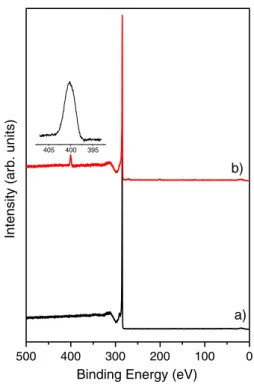
Figure 2. Overview XPS spectra: (a) pristine MWCNTs,
(b) MWCNTs exposed to atomic nitrogen flow in the post-discharge region for 15 min. The inset shows the XPS N 1s spectrum.
Figure1shows a typical micrograph recorded from a treated sample after 45 min in the Ar + N2 microwave plasma. The
excellent condition of the walls of the CNTs indicates that, for the chosen parameters, the plasma treatment does not damage the CNT surface. Normally the outer surfaces of the CNTs are covered by an amorphous carbon layer which is formed during the synthesis. After the plasma treatment, the typical extension of the amorphous layers covering the CNT surface decreased, indicating that this process could be used to clean the CNT surface. Further, experiments are being performed to elucidate this point.
Changes in the chemical nature of the CNT surface caused by exposure to atomic nitrogen were evaluated by analysing the kinetic energy of photoelectrons generated by 3300 eV photons. Figure 2 shows the comparison of XPS spectra recorded on pristine CNTs and on N-functionalized CNTs. The peak at 284.3 eV binding energy, observed in both spectra, arises from photoelectrons emitted from the C 1s core level. The presence of the peak near 399 eV, in the spectrum recorded on the nitrogen-plasma treated sample, proves the effective grafting of nitrogen [16]. The N 1s peak recorded with high energy resolution is shown in the inset of figure 2. The asymmetry of this peak indicates the presence of different nitrogen groups grafted onto the CNT surface. It has been reported that amine, nitrile, oxime and amide groups can be formed by exposing CNTs to a nitrogen-based plasma and the relative concentrations can be tailored by changing plasma parameters [9,11].
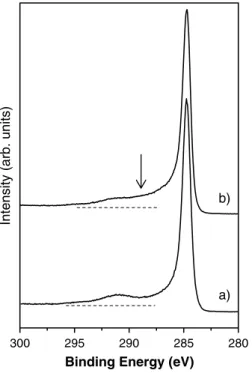
Figure 3 shows a comparison between the C 1s peaks recorded from pristine and treated MWCNTs. Photoelectrons emitted from carbon atoms in the ‘graphite-like’ walls generate the main feature of these spectra at a binding energy of 284.3 eV, i.e. 0.3 eV lower than the value for 2
J. Phys. D: Appl. Phys. 41 (2008) 045202 B Ruelle et al
300 295 290 285 280
Binding Energy (eV)
Intensity (arb. units)
b)
a)
Figure 3. XPS C 1s spectra recorded on (a) pristine CNTs and
(b) atomic nitrogen treated CNTs.
photoelectrons emitted from graphite samples [17]. This shift was associated with the weakening of the C–C bond caused by the redistribution of the electron density with respect to graphene resulting from the curvature of the graphene sheets. The chemical modification produced by the plasma treatment is revealed by the new broad structure near 287.5 eV that is attributed to photoelectrons emitted from carbon atoms belonging to amine, nitrile, amide and oxime groups [9–11].
The C 1s electron energy-loss spectrum has a peak at ∼6.6 eV loss energy (centred at a binding energy of 291.0 eV) for pristine CNTs, corresponding to a π plasmon excitation (figure 3) [17]. A similar loss feature is observable in the spectrum recorded from the treated CNTs. The energy position of the π plasmon loss peak is known to be related to the delocalization of 2p-π electrons; for higher plasmon energy larger electron delocalization is expected; conversely, smaller plasmon energy is related to electronic localization. The absence of loss structures in the C 1s spectrum recorded on the treated MWCNTs, for plasmon energy higher than 6.6 eV energy suggests that the degree of electron delocalization was not increased by grafting nitrogen groups onto the CNT surface. However, an increase in the electron localization cannot be claimed, as in this case photoelectrons emitted from carbon atoms belonging to nitrogen groups would be superimposed to the electron loss structure.
The XPS results reveal that the microwave plasma effectively grafts nitrogen groups onto the CNT surface. The changes on the valence electronic states are revealed in figure 4, which summarizes the UPS valence band spectra obtained from three different samples: pristine MWCNTs and MWCNTs exposed to atomic nitrogen for 5 or 15 min. The valence band spectra were recorded at a photon energy of 55 eV. Due to the random spatial orientation of CNTs in the ‘CNT-film’, the features in the valence band spectra can be
C-N (H) π states C-Cπ states C-Cσ states N lone pair states C-Nπ states C-Nσ states a) b) c) 20 15 10 5 0
Binding Energy (eV)
Intensity (arb. units)
Figure 4. Valence band spectra recorded on (a) pristine MWCNTs
and MWCNTs exposed to atomic nitrogen produced by an Ar + N2
microwave plasma for (b) 5 min and (c) 15 min. The tabs indicate the binding energy of photoelectrons emitted from oxygen atoms [18].
interpreted in terms of the electronic density of states (DOS). The angle averaging avoids any effects of the angle-dependent photoionization cross-sections that might prevent the detection of some electronic states. The valence band structure of the pristine CNTs is essentially the same as that of graphite. The characteristic features arising from the threefold coordination of the C atoms are the 2p-π band near 3.5 eV, the 2p-σ states near 5.5 and 8.0 eV and the mixed 2s–2p hybridized states at 13.6 eV. In the case of MWCNTs, the σ− π hybridization resulting from the formation of the carbon tubes is stronger and this gives rise to the intensity at 11.5 eV binding energy [17]. The feature near 14 eV was reported to be related to oxygen molecules physisorbed on the wall and at the edges of the MWCNTs [18]. In addition to the features observed in the UPS valence band spectrum recorded on the pristine CNTs reference sample, spectra recorded after the N-treatment have a band peaking near 4.2 eV that was attributed to photoelectrons emitted from nitrogen lone pair states (sp2hybridized nitrogen)
[18,19]. The dominant feature centred at 8.5 eV contains contributions from C and N 2p electrons associated with π bonds overlapping the σ -bond feature of the C 2p electrons located at about 7.5 eV (see figure4, pristine sample). The band located at 9.8 eV is generated by photoelectrons emitted from C 2p–N 2p σ -states [17]. A small quantity of oxygen grafted onto the CNT surface was observed (oxygen relative atomic concentration obtained by XPS was equal to 2.8%). The oxygen can be introduced either from the residual gas in the plasma chamber or during the ex situ sample preparation. Photoelectrons emitted from oxygen chemical groups grafted onto the CNT walls were reported to contribute to structures centred at 6.0, 14 and 19 eV [20,21].
J. Phys. D: Appl. Phys. 41 (2008) 045202 B Ruelle et al
4. Conclusion
Photoelectron spectroscopy analysis showed that by exposing MWCNTs to atomic nitrogen generated in a microwave plasma, nitrogen chemical groups can be grafted onto the CNT surface altering the density of electronic states. The observation of the C 1s loss structure on the treated samples suggests that the degree of electron localization is not modified by the treatment. After the plasma treatment, the 2p-π states can no longer be observed and the contribution of 2p-σ states is enhanced. This suggests that the chemical groups introduced by treating CNTs in the post-discharge zone of a microwave Ar + N2 plasma contribute to the 2p-σ states.
The HRTEM images reveal that the atomic nitrogen plasma removes amorphous carbon, but does not damage the surface graphene layer.
Acknowledgments
This work is financially supported by the Belgian Program on Interuniversity Attraction Pole (PAI 6/1 and PAI 6/27) and by DESY and the European Commission under contract RII3-CT 2004-506008 (IASFS). JG is a research associate of NFSR (Belgium). This work is partially supported by the ‘Fonds pour la Formation `a la Recherche dans l’Industrie et dans l’Agriculture (FRIA)’. The authors are grateful to S A Nanocyl (Sambreville, Belgium) for supplying carbon nanotube samples.
References
[1] Ciraci S, Dag S, Yildirim T, G¨ulseren O and Senger R T 2004
J. Phys.: Condens. Matter16 R901–60
[2] Thostenson E T, Ren Z F and Chou Campos T W 2001
Compos. Sci. Technol. 69 1899–912
[3] Ci L J, Ryu Z Y, Jin-Phillipp N Y and Ruhle M 2000 Acta
Mater. 54 5367–75
[4] Collins P G, Bradley K, Ishigami M and Zettl A 2000 Science
287 1801–4
[5] Mickelson E T, Huffman C B, Rinzler A G, Smalley R E, Hauge R H and Margrave J L 1998 Chem. Phys. Lett.
296 188–94
[6] Ago H, Kugler T, Cacialli F, Salaneck W R, Shaffer M S P, Friend R H and Windle A H 1999 J. Phys. Chem. B
103 8116–21
[7] Dettlaff-Weglikowska U, Benoit J-M, Chiu P-W, Graupner R, Lebedkin S and Roth S 2002 Current. Appl. Phys.
2 497–501
[8] Bahr J L, Yang J, Kosynkin D V, Bronikowski M J, Smalley R E and Tour J M 2001 J. Am. Chem. Soc.
123 6536–42
[9] Ruelle B, Peeterbroeck S, Gouttebaron R, Godfroid T, Monteverde F, Dauchot J-P, Alexandre M, Hecq M and Dubois Ph 2007 J. Mater. Chem.17 157–9
[10] Khare B N, Wilhite P, Quinn R C, Chen B, Schingler R H, Tran B, Imanaka H, So C R, Bauschlicher C W Jr and Meyyappan M 2004 J. Phys. Chem.B108 8166–72
[11] Felten A, Bittencourt C, Pireaux J-J, Van Lier G and Charlier J C 2005 J. Appl. Phys.98 074308
[12] Godfroid Th, Dauchot J and Hecq M 2003 Surf. Coating
Technol. 173–174 1276–81
[13] Drube W, Schulte-Schrepping H, Schmidt H-G, Treusch R and Materlik G 1995 Rev. Sci. Instrum.66 1668–70
[14] Drube W, Grehk T M, Treusch R and Materlik G 1998
J. Electron Spectrosc. Relat. Phenom.88 683–687
[15] Johnson R L and Reichardt J 1983 Nucl. Instrum. Methods
Phys. Res.208 791–6
[16] Beamson G and Briggs D 1992 High Resolution XPS of
Organic Polymers: The Scienta 300 Database (Chichester:
Wiley)
[17] Chen P, Wu X, Sun X, Lin J, Ji W and Tan K L 1999 Phys.
Rev. Lett.82 2548–51
[18] Lim S C, Jo C S, Jeong H J, Shin Y M, Lee Y H, Samayoa I A and Choi J 2002 Japan. J. Appl. Phys.41 5635–9
[19] Bj¨orkqvist M, G¨othelid M, Grehk T M and Karlsson U O 1998
Phys. Rev. B57 2327–33
[20] Alvarez F and dos Santos M C 2000 J. Non-Cryst. Solids
266–269 808–14
[21] Felten A, Ghijsen J, Pireaux J J, Johnson R L, Whelan C M, Liang D, Van Tendeloo G and Bittencourt C 2007 J. Phys.
D: Appl. Phys.40 7379-82