HAL Id: hal-01816372
https://hal.laas.fr/hal-01816372
Submitted on 5 Apr 2019
HAL is a multi-disciplinary open access
archive for the deposit and dissemination of
sci-entific research documents, whether they are
pub-lished or not. The documents may come from
teaching and research institutions in France or
L’archive ouverte pluridisciplinaire HAL, est
destinée au dépôt et à la diffusion de documents
scientifiques de niveau recherche, publiés ou non,
émanant des établissements d’enseignement et de
recherche français ou étrangers, des laboratoires
Fabrication and characterization of mechanical
resonators integrating microcontact printed PZT films
Daisuke Saya, Denis Dezest, Thierry Leichle, Fabrice Mathieu, Liviu Nicu,
Olivier Thomas, Aaron Welsh, Susan Trolier-Mckinstry
To cite this version:
Daisuke Saya, Denis Dezest, Thierry Leichle, Fabrice Mathieu, Liviu Nicu, et al.. Fabrication and
characterization of mechanical resonators integrating microcontact printed PZT films. 2017 Joint
IEEE International Symposium on the Applications of Ferroelectric (ISAF)/International Workshop
on Acoustic Transduction Materials and Devices (IWATMD)/Piezoresponse Force Microscopy (PFM),
May 2017, Atlanta, United States. �10.1109/ISAF.2017.8000219�. �hal-01816372�
Fabrication and characterization of mechanical
resonators integrating microcontact printed PZT films
Daisuke Saya, Denis Dezest, Thierry Leïchlé,
Fabrice Mathieu, Liviu Nicu
LAAS-CNRS University of Toulouse Toulouse, France
Olivier Thomas
LSIS/INSM Lille, FranceAaron J. Welsh, Susan Trolier-McKinstry
The Pennsylvania State University PA, USA
Abstract—We report on the fabrication and characterization of lead zirconate titanate (PZT)-coated cantilever resonators for the realization of piezoelectric nanoelectromechanical systems (NEMS) with integrated actuation and detection capabilities. PZT is deposited by microcontact printing, resulting in a relatively thin PZT film without deterioration of its piezoelectric properties induced by etching damage. The cantilever fabrication process is based on stepper ultraviolet lithography and standard micromaching. Electrical characterization was carried out with a dedicated electrical set-up enabling the devices’ resonance frequency to be detected through the piezoelectric response. These characterizations validate the simultaneous actuation and detection capability of the PZT layer. Finally, modeling of the PZT cantilever results in the estimation of the piezoelectric coupling coefficient d*31. We have found excellent large signal
d*31 of around 200 pm/V, even for PZT cantilevers with reduced
dimensions.
Keywords—NEMS; piezoelectricity; microcontact printing; PZT; cantilever; resonator
I. INTRODUCTION
With advances in nanotechnology, the realm of electromechanical systems has witnessed the emergence of nanoelectromechanical systems (NEMS) over the last decade. The significant enhancement of devices’ performance when scaling down the size has been widely reported for NEMS-based resonators [1]-[4][7]-[9]. Especially, mechanical resonators with free-standing structures consisting of nanometer scale cantilevers or bridges show great performance in mass sensing for gases [3] and biomolecules [4].
So far, piezoelectric films, which translate mechanical energy into electrical and vice-versa, have already been widely used for microelectromechanical systems (MEMS) transduction [5][6]. Piezoelectrics require relatively low actuation voltage and also offer a sensing capability, resulting in devices that are compact, thus potentially portable. Employing piezoelectric films for NEMS could be even more advantageous for high integration potential of both actuation and sensing capabilities [7]-[9]. To this aim, deterioration of the piezoelectric characteristics with reduced sizes should be
overcome. Indeed, when patterning PZT films deposited by sputtering onto NEMS resonators, deterioration of their characteristics is difficult to avoid [8][9]. Recently, microcontact printed PZT films were found to retain their characteristics with reduced lateral dimensions and reduced thicknesses [10].
In this paper, cantilever resonators with integrated PZT thin film deposited by microcontact printing method were fabricated and characterized. The PZT cantilevers were assessed for piezoelectric excitation and detection. The PZT cantilevers were then modeled in order to estimate their piezoelectric coefficient.
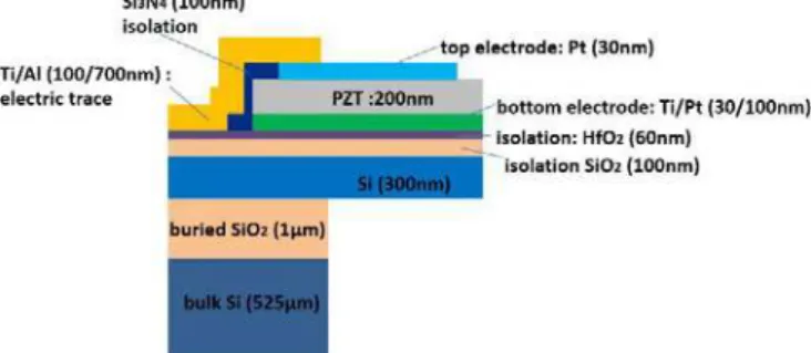
II. FABRICATION A. Cantilever chip design
We designed two types of cantilever structures in order to study possible dimentional effects upon PZT properties: the short version is 35 µm long and 5 µm wide and the long version is 150 µm long and 30µm wide. Each cantilever is a
multilayer composed of 300 nm thick Si, 100 nm thick SiO2,
60 nm thick HfO2 for isolation, 30 nm/100 nm thick Ti/Pt
layers as the bottom electrode, 200 nm thick microcontact printed PZT layer, and 30 nm thick Pt top electrode, as shown in Fig. 1. An unreleased cantilever with exactly the same structure was integrated onto the same chip, serving as a reference to compensate the static capacitance of the piezoelectric stack during electrical characterization as described in section III.
B. Fabrication of PZT cantilevers
Fabrication of PZT cantilevers started with an SOI (silicon on insulator) wafer, with top Si thickness of 340nm, buried SiO2 1µm and bulk Si 525µm. An ultraviolet (UV) stepper
photo repeater (I-line FPA 3000 Canon Inc.) was used for lithography since high resolution and precise alignment are desirable for top-down NEMS fabrication.
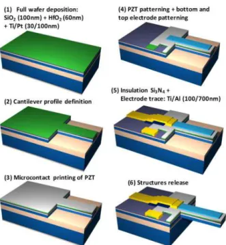
First, thermal oxidation was used for isolation (film thickness, 100 nm), followed by atomic layer deposition of HfO2 with a thickness of 60 nm which served as a barrier
against Pb diffusion. Then, 30 nm/100 nm thick Ti/Pt layers were deposited by sputtering to serve as the bottom electrode (Fig. 2(1)). Next, the cantilever profile was defined by successive reactive ion etching of Pt, Ti, HfO2, SiO2 and top Si
until the buried SiO2 appeared (Fig. 2(2)).
Fig. 2. Fabrication process of the microcontact printed PZT microcantilever. The colors used for each material corresponds to those of Fig. 1.
Microcontact printing of PZT was then performed (Fig.2(3)). To this aim, PZT sol-gel solution (10 wt%, 1 %Mn doped, with atomic percent Pb=110%, Zr=30%, Ti=70%, Mn= 1%), was prepared and spin-coated on polydimethylsiloxane (PDMS) stamp. Then, PZT was printed on the entire surface of the chip by hand, followed by annealing at 350 °C for 300 sec and rapid thermal annealing at 650 °C for 60 sec. This printing process was repeated three times to achieve a final 200 nm thickness. Since the cantilever profile with bottom electrode was defined before PZT printing as shown in Fig. 2(2), there was no need for precise alignment during PZT printing for PZT patterning on the cantilever.
In order to connect the bottom electrode, PZT was patterned by wet etching with buffered hydrofluoric acid (BOE), followed by Ti/Pt bottom electrode patterning by reactive ion etching. Then, the 30 nm thick Pt top electrode was deposited by lift off (Fig.2(4)).
The next step was dedicated to patterning the ground plane, in order to allow the top Si layer of the SOI wafer to be electrically grounded. This process consisted first in etching the HfO2 and SiO2 films to reveal the top Si layer everywhere
on the chip surface, except at the electrode and cantilever locations, and then to deposit Ti/Al. As discussed in section III, this step eliminated the parasitic capacitance between the electrodes and the top Si layer.
Next, a 100 nm thick Si3N4 insulating film was patterned by
lift-off to avoid electrical shorts between the bottom electrode and electric traces subsequently realized by 100 nm/ 700 nm Ti/Al lift-off patterning (Fig. 2(5)). Finally, backside etching for cantilever release was performed by deep reactive ion etching of the thick Si handle wafer with a thick photoresist mask of AZ40XT 40 µm followed by etching of the buried 1 µm SiO2 layer (Fig. 2(6)).
Fig. 3 shows SEM images of the PZT cantilevers.
Fig. 3. SEM images of the microcontact printed PZT microcantilevers. (a) Short cantilever, (b) Long cantilever.
III. CHARACTERIZATION
A. Electrical setup
A schematic of the electrical set up is shown in Fig. 4 [6].
A sinusoidal voltage V1 was applied across the electrodes on
the piezoelectric stack of a free-standing cantilever. An
opposite voltage -V2 was applied onto an unreleased
mechanical structure of the same dimensions which served as a reference to reduce the effect of the static capacitance of the PZT layer. The charges generated by the two structures were collected by the common bottom electrode and were amplified through a charge amplifier with a gain of 1 pC/V. The signal was then injected into a demodulator to extract both amplitude and phase.
On the chip, the top Si layer was grounded to eliminate charges generated by the parasitic capacitances C1 and C2,
while, charges from Cs were compensated by the reference,
where:
C1: parasitic capacitance between the top electrode
C2: parasitic capacitance between the bottom
electrode trace line and the top Si layer of the SOI Cs: static capacitance of the PZT (dielectric) layer
sandwiched between the top and bottom electrodes
Cmot: motional capacitance corresponding to the
charges generated by the PZT layer during the resonator motion due to the piezoelectric direct effect
Fig. 4. Schematic sketch of the electrical detection scheme.
B. Resonance frequency measurement
Resonance frequency measurement of the PZT cantilevers were carried out with the electrical set-up mentioned above. Fig. 5 shows the piezoelectric response (generated charges) of the fundamental mode resonance frequency in air before poling
treatment. The actuation voltage V1 was set to 700 mV for the
short cantilever (a) and 100 mV for the long cantilever (b).
Fig. 5. Resonance spectrum of the piezoelectric cantilever before poling treatment: (a) the short cantilever, (b) the long cantilever.
The measured fundamental mode of the short cantilever (a) is 467.5 kHz, which is consistent with simulation results of 467.1 kHz (the difference is just 0.1%). In the case of the long cantilever, the measured fundamental mode is 18.2 kHz while the simulated one is 25.5 kHz (i.e., a difference of 40%). This large discrepancy is believed to be a consequence of a decrease in the cantilever’s thickness due to overetching during
fabrication. The generated charge at the resonance peak is about 1.4 fC for the short cantilever (a) and 120 fC for the long cantilever (b), which validates the simultaneous capability of actuation and detection of the cantilevers with microcontact printed PZT.
To improve the PZT properties, thermal poling of the PZT was performed by applying 3V between the top and bottom electrodes at a temperature of 150°C for 15 minutes [11]. After poling, charges generated at the resonance peak were found to increase up to 10 fC with decreased actuation voltage of 100 mV for the short cantilever. For the long cantilever, the amplitude of resonance peak increased by 33 %. The effect of poling was much more remarkable in the case of the short cantilever.
Fig. 6. Piezoelecric responses of (a) the short and (b) the long cantilever as a function of the actuation voltage after poling treatment.
Fig. 7. Linear slopes of the generated charges at resonance as a function of the actuation voltage after poling treatment: (a) The short cantilever, (b) the long cantilever.
Resonance spectra obtained from the generated charges with variation of the actuation voltage after poling treatment are plotted in Fig. 6, showing excellent linear responses. The
applied voltages V1 varied from 25 mV to 300 mV for the short
cantilever (a) and from 25 mV to 125 mV for the long cantilever (b). The estimated quality factor are: 185 for the
Rf Cmot Cs Charge amplifier 10MΩ 1pF -+ C1 C2 C’mot R’ f C’2 C’s C’1 PZT cantilever PZT reference Bottom electrode Top electrode - V2 V1 Bottom electrode Top electrode Grounding of the top Si layer PZT cantilever PZT reference Top electrode Top electrode PZT PZT Bottom electrode - V2 V1 Cc= 1pF -+ Vout(t) HfO2insulation
short cantilever (a) and 66 for the long one (b). Linear slopes of the generated charges at resonance peak as a function of actuation voltage are plotted in Fig. 7.
C. Estimation of the piezoelectric coupling coefficient The PZT cantilever was modeled as a laminated beam [12][13]. If a sinusoidal voltage signal V(t) = V1cosωt is
applied on the top electrode of the cantilever, the part of the charge generated by the piezoelectric layer is written as q(t) = qmcos(ωt+φ). Then, the motional capacitance is theoretically
[9][12][13]:
mot= = (1)
where, Q is the quality factor, L the cantilever length and m its mass per unit length. is the modal piezoelectric coupling coefficient, which can be analytically computed as a function of the geometrical and material properties of the laminated beam’s cross section (see [12][13] for details) and which is proportional to the material piezoelectric coupling coefficient d*31. Experimental values of mot are obtained with the ratio
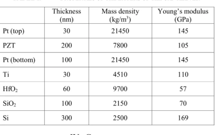
between qm and V1 (Fig. 7). By comparing them with
theoretical values computed with the material properties gathered in Tab. 1 [9][14][15], a large signal piezoelectric coefficient d*31: 163 pm/V is calculated for the short cantilever
and 221 pm/V for the long cantilever. The estimated values of d*31 of the cantilevers with microcontact printed PZT are
comparable to small signal numbers for bulk PZT ceramics [16]. Even for the shorter cantilever with reduced dimension of 5 µm in width and 35 µm in length, PZT keeps its rather high value of large signal d*31.
TABLE I. PROPERTIES OF THE LAYERS OF THE CANTILEVER
Thickness
(nm) Mass density (kg/m3) Young’s modulus (GPa)
Pt (top) 30 21450 145 PZT 200 7800 105 Pt (bottom) 100 21450 145 Ti 30 4510 110 HfO2 60 9700 57 SiO2 100 2150 70 Si 300 2500 169 IV. CONCLUSIONS
Cantilevers were fabricated with 200 nm thick microcontact printed PZT films by stepper based UV lithography and miocromachining. The cantilever resonance frequencies were detected by piezoelectric readout. The capability of simultaneous excitation and detection of the PZT cantilevers was validated. After poling, the piezoelectric properties of the PZT films were increased. The PZT cantilever was modeled to estimate the large signal piezoelectric coefficient d*31. Hence, ultra thin microcontact printed PZT
films offer promising transduction schemes for piezoelectric NEMS with integrated actuation and sensing capabilities.
ACKNOWLEDGMENTS
The French General Delegation for Armament and the French National Agency for Research (grant ANR/PNANO 2008, project NEMSPIEZO ‘ANR-08-NANO-015’), and a National Security Science and Engineering Faculty Fellowship are gratefully acknowledged for financial support.
REFERENCES
[1] H.G. Craighead , “Nanoelectromechanical systems,” Science, 2000, vol. 290, pp. 1532–1535.
[2] M. L. Roukes, “Nanoelectromechanical systems face the future,” Phys. World, 2001, vol. 14, pp. 25–31.
[3] J. Chaste, A. Eichler, J. Moser, G. Ceballos, R. Rurali and A. Bachtold, “A nanomechanical mass sensor with yoctogram resolution,” Nat. Nanotech., 2012, vol. 7 pp. 301–304.
[4] B. Ilic, Y. Yang, K. Aubin, R. Reichenbach, S. Krylov, and H. G. Craighead, “Enumeration of DNA Molecules Bound to a Nanomechanical Oscillator,” Nano Letters, 2005, vol. 5, pp. 925-929. [5] S. Trolier-McKinstry and P. Muralt, “Thin film piezoelectrics for
MEMS,” J. Electroceram. 2004, vol.12, pp. 7–17.
[6] F. Mathieu, F. Larramendy, D. Dezest, C. Huang, G. Lavallee, S. Miller, C.M. Eichfeld, W. Mansfield, S. Trolier-McKinstry, L. Nicu, “Reducing parasitic effects of actuation and sensing schemes for piezoelectric microelectromechanical resonators,” Microelec. Eng., 2013, vol. 111, pp. 68–76.
[7] R. B. Karabalin, M. H. Matheny, X. L. Feng, E. Defaÿ, G. Le Rhun, C. Marcoux, S. Hentz, P. Andreucci and M. L. Roukes, “Piezoelectric nanoelectromechanical resonators based on aluminum nitride thin films,” Appl. Phys. Lett. 2009, vol. 95, 103111.
[8] S. Guillon, D. Saya, L. Mazenq, J. Costecalde, D. Remiens, C. Soyer, L. Nicu, “Lead Zirconate Titanate Nanoscale Patterning by Ultraviolet-Based Lithography Lift-Off. Technique for Nano-Electromechanical. System Applications,” IEEE Trans. Ultrason. Ferroelectr. Freq. Control, 2012, vol. 59, pp. 1955-1961.
[9] D. Dezest, O. Thomas, F. Mathieu, L. Mazenq, C. Soyer, J. Costecalde, D. Remiens, J.-F. Deü, L. Nicu, “Wafer-scale fabrication of self-actuated piezoelectric nanoelectromechanical resonators based on lead zirconate titanate (PZT),” J. Microelec. Microeng., 2015, 25 (3), pp. 35002-35013.
[10] A.J. Welsh, R.H.T. Wilke, M.A. Hickner, S. Trolier-McKinstry, “Low-Cost, Damage-Free Patterning of Lead Zirconate Titanate Films,” J. Am. Ceram. Soc., 2013, vol. 96, pp. 2799-2805.
[11] J.F. Shepard Jr, P.J. Moses, S. Trolier-McKinstry, “The wafer flexure technique for the determination of the transverse piezoelectric coefficient (d31) of PZT thin films,” Sens. & Act. A: 1998, vol. 71, pp.
133-138.
[12] J. Ducarne, O. Thomas, and J.-F. Deü, “Placement and dimension optimization of shunted piezoelectric patches for vibration reduction,”. J. Sound Vib., 2012, 331(14) pp. 3286–3303.
[13] O. Thomas, B. Legrand, and C. Fuinel, “Optimization of length and thickness of smart transduction layers on beam structures for control and M/NEMS applications”, SMASIS 2015 Colorado Springs, USA, Sept. 2015, pp. 8857.
[14] D. Das, L. Sanchez, J. Martin, B. Power, S. Isaacson, R. G. Polcawich, and Ioannis Chasiotis, “Control of mechanical response of freestanding PbZr 0.52 Ti 0.48 O 3 films through texture,” Appl. Phys. Lett. vol. 109, 2016, pp. 131905.
[15] http://www.makeitfrom.com/material-properties/Hafnia-Hafnium-Oxide-HfO2
[16] POLYTEC PI. Piezoelectric ceramic products. http://www.piceramic.com, 2006 (Internet).