HAL Id: tel-03207382
https://tel.archives-ouvertes.fr/tel-03207382
Submitted on 24 Apr 2021Micro patterning of complex Waveguide Resonant
Gratings (WRG)
Erieta-Katerina Koussi
To cite this version:
Erieta-Katerina Koussi. Micro patterning of complex Waveguide Resonant Gratings (WRG). Optics / Photonic. Université de Lyon, 2020. English. �NNT : 2020LYSES027�. �tel-03207382�
N° ordre NNT: 2020LYSES027
THESE de DOCTORAT DE L’UNIVERSITE DE LYON
Opérée au sein du
Laboratoire Hubert-Curien
Ecole Doctorale N° 488
Sciences Ingénierie Santé SIS Spécialité: Optique, Photonique, Hyperfréquences
Soutenue publiquement le 22/10/2020 par :
Erieta Katerina KOUSSI
Micro patterning of complex
Waveguide Resonant Gratings (WRG)
Devant le jury composé de :
Stéphane CALVEZ CR CNRS, HDR, LAAS, Toulouse Rapporteur Frédéric DUMAS-BOUCHIAT Professeur, IRCER, Université de Limoges Rapporteur Marwan ABDOU AHMED Docteur HDR, IFSW, University of Stuttgart Examinateur Laurent DUBOST Ingénieur Chercheur, HEF/IREIS, Saint-Etienne Invité Christophe DONNET Professeur, LabHC, Université Jean Monnet, Saint-Etienne Examinateur Florent BOURQUARD Maître de Conférences, LabHC, Université Jean Monnet, Saint-Etienne Co-directeur de thèse Isabelle VERRIER CR CNRS, HDR, LabHC, Saint- Etienne Invitée
Δῶς μοι πᾶ στῶ καὶ τὰν γᾶν κινάσω
“Give me somewhere to stand and I will move the earth”
Archimedes, 287-212 BC, Mathematician, physicist, engineer, inventor and astronomer
Acknowledgements
This dissertation, the fruit of three years of hard work and perseverance, is fully dedicated to my family, partner, friends, colleagues and mentors as a token of gratitude for their continued contribution and support. First, I would like to thank my Mom Alexandra and my Dad Sotiris not only for their constant encouragement but also for their unwavering love and ideals that they passed on to me during my life. In addition, I owe special thanks to my boyfriend Georgios Aznaouridis who believed in me and strongly motivated me not to quit my effort, helping me to overcome my daily obstacles. His love and patience strengthened the faith on me and inspired me to be better every day. I would also like to acknowledge my friend Elena who is always there when I need her and who pushed me to write down my thesis during the last summer despite the ups and downs we have spent together. Throughout the years of my thesis, I had the privilege of meeting some amazing people, who all had a part in shaping both me and my work. I would like to thank my friend and colleague Andrei Ushkov, who is an inexhaustible source of knowledge and who was always willing to explain anything I could not understand. My friend and colleague Rim Faraj with whom we pushed each other to achieve more. The other office colleagues, Maria Usuga, Marion Hochedel, Hugo Bruhier, Arnaud Valour, Julie Dutems, Emilie Laffond, Ratish Rao, members of the grating group, who made everyday life enjoyable.
My sincerest thanks to my thesis tutor, Yves Jourlin, who supervised me and always encouraged me to push my boundaries and strive for more. I am especially grateful to my co-supervisor and friend Florent Bourquard, who offered me the opportunity to work in the Hubert Curien Laboratory and was constantly present and scientifically curious like I was in the project we started together. Within this project, I would like to thank Laurent Dubost, collaborator of the HEF Company who offered me a good expertise on the magnetron-sputtering machine. Moreover, I would like to recognize Isabelle Verrier who took me under her wing and provided valuable guidance in the most critical points of this thesis. Finally, I would like to acknowledge
Contents
General Introduction………1
1.1 Introduction ... 7
1.2 Historical Review ... 7
1.3 Principle of Diffraction Grating ... 13
Profile of diffraction gratings ... 13
Grating Illumination ... 14
Diffraction regimes ... 15
Diffracted orders and Grating Equation ... 16
Representation in the reciprocal space with Ewald Sphere ... 17
Subwavelength Gratings ... 19
1.4 Diffraction Gratings under polarized light ... 20
Polarization States ... 20
Diffraction grating dependence on light polarization ... 22
1.5 Waveguide Resonant Grating ... 23
Structure of a Waveguide Resonant Grating (WRG)... 23
Planar Waveguide ... 25
1.6 Resonance Study ... 29
Resonance Principle ... 29
Mode Coupling ... 31
Polarization dependence of the resonance response ... 39
Dimensioning resonance with optogeometrical grating waveguide parameters ... 40
True-Modal Method (TMM) ... 45
C-Method ... 46
1.8 Conclusion ... 46
Introduction ... 54
Introduction to photolithography and overview protocol for WRG fabrication... 54
Characteristics and preparation of the resists ... 57
Photosensitive Resists ... 58
Positive Resist ... 58
Negative Resist: TiO2/BzAc Solgel ... 62
Deposition methods and sample preparation ... 68
Choice and preparation of the substrate ... 68
Dip Coating ... 69
Spin Coating ... 72
Thermal treatment of the layers ... 74
Exposure Techniques ... 75
Laser Interferential lithography (LIL) or Holography set-up ... 75
Mask lithography ... 77
Development and post-treatment steps ... 78
Development ... 78
Oxygen Plasma ... 80
Conclusion ... 81
Principle of the tube exposure with the phase mask ... 92
Study of the cylindrical WRG ... 94
Design principle of the cylindrical WRG ... 94
Modelling of the cylindrical WRG ... 95
Fabrication of the resonant structure inside the tube ... 97
Substrate pre-treatment ... 97
TiO2 solgel waveguide and resist deposition ... 97
Cylindrical Photolithography ... 98
Structural characterization of the tube, the waveguide layer and the grating ... 101
Structural characteristics of the irradiated tube... 102
FIB (Focused Ion Beam) ... 102
Period measurement ... 104
Optical Resonant excitation ... 106
Resonance excitation ... 106
Effect of the incident beam polarization ... 107
Optical set-up ... 109
Results and discussion ... 112
Conclusion ... 115
4.1 Introduction ... 118
4.2 VO2 characteristics and applications ... 119
4.2.1 General Characteristics of Vanadium Dioxide (VO2) ... 119
4.2.2 Applications of VO2 ... 121
4.2.3 Intrinsic properties of Vanadium Dioxide (VO2) ... 125
4.2.4 VO2 phase diagram ... 127
4.2.5 General review in VO2 thin film formation ... 127
4.3.1 Principle of PLD ... 129
4.3.2 Review on PLD-VO2 synthesis ... 131
4.3.3 Advantages and Drawbacks of PLD technique... 132
4.3.4 PLD experimental process ... 133
4.3.5 Parametric study of the thermal switch ... 135
4.3.6 Characterization of the VO2 layer ... 140
4.4 Magnetron Sputtering ... 143
4.4.1 Principle of Magnetron Sputtering ... 143
4.4.2 Review on Magnetron sputtering -VO2 synthesis ... 146
4.4.3 Advantages and Drawbacks of Magnetron Sputtering technique ... 148
4.4.4 Magnetron Sputtering experimental process... 148
4.4.5 Characterization of bilayer Si3N4/VO2 ... 150
4.5 Conclusion ... 151
Introduction ... 162
Overview on VO2 based sensors ... 163
Designs of VO2 embedded structures fabricated by magnetron sputtering or PLD method ... 168
Design of the structure with VO2 film synthesized by magnetron sputtering (1st approach) ... 170
Design of the structure with VO2 film synthesized by PLD (2nd approach) ... 176
Fabrication and structural characterization for PLD and magnetron sputtering based designs ... 181
Results and discussion ... 186
Conclusion ... 187
Résumé
Cette thèse de doctorat intitulée “Micro structuration de Réseaux Résonants complexes” étudie les dispositifs de détection optique, qui impliquent diverses techniques de photolithographie et outils de micro/nanotechnologie pour leur fabrication. Ces dispositifs, dans leur forme classique, consistent en un réseau de diffraction formé de lignes microscopiques gravées périodiquement sur une surface photosensible, qui est déposée sur une couche diélectrique, le guide d'onde. Les deux couches sont supportées par un substrat. Pour activer les fonctions de détection, le réseau de diffraction doit être extrêmement sélectif, c'est-à-dire qu'il doit avoir la capacité de rejeter toutes les composantes spectrales reçues, en ne sélectionnant qu’une seule longueur d'onde pour la coupler au guide d'onde. Après le découplage, une réflexion dite résonante liée à sa très grande amplitude et sélectivité spectrale et angulaire se produit. Différents types de composants en fonction de l'application envisagée peuvent être réalisés sur différents types de substrats, matériaux ou géométries (plan, cylindrique).
L'un des projets de cette thèse consiste à concevoir des WRG (Waveguide Resonant Gratings) sur les parois intérieures d'un tube pour coupler les modes TE et TM à l’intérieur du guide d’onde. La fabrication est réalisée par un masque de phase radial spécialement conçu, tandis que la fonction optique est mise en évidence en utilisant un miroir conique, capable de réfléchir la lumière de manière isotrope pour l'excitation des modes.
De plus, des matériaux innovants peuvent être utilisés pour leur intégration dans des structures résonantes planaires. L'un des matériaux à l'étude pour le deuxième type de composant est le dioxyde de vanadium (VO2), qui subit respectivement des transitions de phase de premier ordre
(isolant vers métal) à basses et hautes températures. La fabrication d'un composé aussi délicat est complétée par deux méthodes de synthèse différentes, le dépôt par laser pulsé et la pulvérisation cathodique magnétron. La capacité d'induire une résonance en déclenchant thermiquement le dispositif est destinée aux applications de sécurité laser afin d'éviter l’endommagement lors d'une surchauffe.
Abstract
This PhD thesis entitled “Micro patterning of complex Waveguide Resonant Gratings (WRG)” studies the optical sensing devices, which involve various photolithography techniques and nanotechnology tools with clean room processes for their fabrication. These devices, in their classic form, consist of a diffraction grating formed by microscopic lines engraved periodically on a photosensitive surface, which is deposited on a dielectric layer, the waveguide. Both layers are supported by a substrate. To enable sensing functions, the diffraction grating must be extremely selective, i.e. it must have the ability to reject all the received spectral components, while selecting only one wavelength to couple it into the waveguide. After the out coupling, a reflection with a very large amplitude and great finesse occurs. Different types of components depending on the intended application can be produced on different types of substrates, materials or geometries (plane, cylindrical).
One of the projects of this thesis engineers WRG on the interior walls of a tube to couple TE and TM modes into the waveguide. The fabrication is achieved by a specially designed radial phase mask, whereas the optical function is highlighted by the use of a conical mirror, able to reflect light isotropically for mode excitation.
In addition, innovative materials can be used for their integration into flat WRG. One of the materials under study for the second type of device is the Vanadium Dioxide (VO2), which
undergoes first-order phase transitions (Insulator to Metal) at low and high temperatures respectively. The fabrication of such a delicate compound is completed by two different synthesis methods, the Pulsed Laser Deposition and Magnetron Sputtering. The ability to induce resonance by thermally triggering the device is intended for laser safety applications to avoid damage during overheating.
General Introduction
The “Micro patterning of complex Waveguide Resonant Gratings (WRG)” PhD thesis has been financed by the LabEX MANUTECH SISE (ANR-10-LABX-0075) of Université de Lyon, within the program “Investissements d'Avenir” (ANR-11-IDEX-0007) operated by the French National Research Agency (ANR) ANR project.
This PhD Thesis has been proposed in the project R2EX (Design and realization of resonant gratings with extreme efficiency) within the Axis 3 (Perception Engineering & White Light Processing) of the Labex MANUTECH SISE. The aim of the Axis 3 of the Labex MANUTECH SISE is to develop quantitative characterization methods (adjusted for example to human perception), but beyond that, to develop real materials and surface engineering for perceptual specifications or specific interactions with light. This project was in close collaboration between the Laboratory Hubert Curien and HEF /IREIS Company.
The objective of this thesis is to develop sensors for optical filtering applications using WRG (Waveguide Resonant Grating) configurations. These latter are proposed with complex geometries in cylindrical form or with integrated layers of attractive materials (VO2) in
waveguides for optical resonances.
Waveguide resonant gratings or resonant waveguide gratings, guided mode resonant gratings or also waveguide-mode resonant gratings have been known for a long time, since the beginning of the eighties. They are used in the fields of lasers (wavelength filtering, polarization control, transverse mode control…), sensors (bio, chemical sensors), photo-detectors, color rendering and color effects, energy (solar cells) … Most of the time, Waveguide Resonant Gratings combine surface microstructures and dielectric thin films to exploit the so-called 100% efficiency resonant (abnormal) reflection for one wavelength (and one polarization), in opposition to the so-called abnormal and extraordinary transmission when one describes plasmonics based waveguide in a metallic thin film, embedded in a dielectric film. WRGs use periodic microstructures, such as gratings and high refractive index for the dielectric thin film. In order to couple wave-guided modes in the thin film, gratings are high spatial frequency gratings to only use the 0th order that is a subwavelength grating. Even though WRG are well known theoretically, they are not extensively exploited in industry and in everyday life. One of the reasons, which could explain such fact, is the difficulty to fabricate high efficiency and
of the WRG, many parameters must be well controlled: grating parameters (duty cycle, depth, roughness, homogeneity….), and waveguide parameters (thickness, refractive index, roughness…).
Within this PhD thesis, we propose to exploit two separate approaches using WRG. The first one deals with a perfect circular grating, printed inside the inner surface of a tube, in order to measure resonant reflection considering an infinite WRG, in a complex measurement set-up. The grating has been fabricated using the cylindrical lithography-based phase mask technique developed a few years ago at the Laboratoire Hubert Curien. The second approach is well known and exploit thermally activated waveguides, using VO2 phase change material. In the
latter case, the idea is to control the resonant reflection thermally and to propose an ingenious design. In both approaches, modeling, design, fabrication and measurement are well described and discussed.
The manuscript consists of 5 chapters:
Chapter 1 introduces the basic principles of WRG configurations with a comprehensive analysis of their structure and operation. In the first part, a historical review describes Wood‘s first observations of the resonance phenomenon, which was initially identified as an anomaly, and continues with the long-term study of its understanding and exploitation in sensing. Such resonances, which correspond to sharp peaks in reflection, occur once the incident light is coupled to the waveguide modes propagating in the waveguide layer. To direct incident light in the waveguide region a corrugation on its top is necessary. The space between the corrugation grids is called period and must be of the order of micrometers and below to generate fine optical responses in the range of the visible and near infrared. These structures dependent largely on the angle and polarization of the incident light, but also on the effective index of the layers and structural characteristics. The aforementioned parameters, except polarization, are involved in the grating equation, which calculates mathematically the diffraction orders that are expected to be supported by the structure, while a graphical geometrical representation using the Ewald Sphere illustrates the direction of the modes. For additional optimization, dedicated programs as “MC Gratings” and Modal Collinear method predict the final features of the resonance
which consists of a waveguide and a diffraction grating. To fabricate thin layers with well-controlled properties, we used a negative-based sol gel resist for waveguide deposition and a positive S1805 photoresist for grating patterning. The protocol of the sol gel is developed at Hubert Curien Laboratory to be adaptable to waveguide films. Spin and dip coating techniques were used for layer deposition, compatible with flat and cylindrical substrates respectively. The micro patterning of the positive photoresist is performed with a photolithography process; laser interferential lithography obtained from the contribution of two optical fibers for planar structures and phase mask lithography for cylindrical devices as it will be discussed below. In both cases, the interferogram becomes immediately visible after the development in the TMAOH (trimethylamine N-oxide). As presumed, each treatment step is highly dependent on ambient temperature and conditions and requires clean room elaboration for contaminant free and well-structured patterns. At the end of the process and in case of a slightly altered grating, a plasma technique can be implemented to adjust the thickness to the original simulated one.
Once the techno-optical expertise has been gained, Chapter 3 proceeds with the presentation of the one of the main works of this dissertation: the WRG fabrication on the inner walls of a miniaturized cylindrical substrate. This project presents an 8-mm diameter tube of fused silica that is structured on its inside cavity with a thin sol gel waveguide and a positive photoresist grating. The patterning of the grating is performed by a radial phase mask, which is conceived, designed and fabricated exclusively for cylindrical grating fabrication. This technological compound is specially designed to diffract only the ±1 orders transversally to the tube axis while extinguishing the 0th order parallel to it. After a proper alignment of the tube with the
radial phase mask, the interference of the orders leads to a stitchingless cylindrical grating that appears upon TMAOH development (Figure 1).
Figure 1: Micro patterned grating on a TiO2 sol gel-made waveguide layer in the hollow of a fused
silica tube.
The resonance efficiency of the prepared device is characterized with the aid of a 90° apex conical mirror that enables the transformation of plane waves into cylindrical waves. The mirror
is inserted to the hollow of the tube and the incident light after being circularly polarized, impinges on the mirror and is reflected holistically to the annular WRG. At the end of the mode coupling, the expected resonances in TE and TM polarizations in the near infrared range are measured by an optical spectrometer. The device is planned for gas or liquid sensing applications.
Chapter 4 displays an extensive study on the fabrication of VOx (with x as close to 2 as possible)
layers. The VO2 chemical element is a high interest element that undergoes an insulator to metal
(IMT) transition at a critical temperature of T~68°C, with simultaneous electrical and optical switching in the near infrared. Usually in the form of thin films, VO2 is attempted to be
manufactured by two methods: The Pulsed Laser Deposition (PLD) developed at the Hubert Curien Laboratory and the pulsed DC magnetron sputtering technique performed at the HEF Group Company (IREIS). The first method in combination with the Rapid Thermal Annealing (RTA) aimed to lower as much as possible the annealing temperature to be compatible with several substrates. Thus, various substrates are tested as well as oxygen pressures during deposition and annealing, temperature and annealing time whose effects on VO2 synthesis is
investigated (Figure 2).
Figure 2: Various substrates that have undergone the effect of oxygen pressure during deposition and of annealing process.
The second method also succeeded in forming a VO2 layer with a homemade vacuum furnace
on SiO2 substrates. Upon completion of the VO2 thin films Raman, AFM, and SEM
measurements are performed. Systematically, the optical transmission and hysteresis width between cold and hot states, phase transition temperature and transmittance amplitude are
According to the synthesis method, two designs are proposed. The PLD VO2 film is deposited
in the proximity of a TiO2 anatase film to form a bilayer waveguide with almost equal refractive
indices that enhance the total reflection criteria. An upper positive photosensitive layer is patterned on the waveguide and the overall is supported by a SiO2 substrate. This configuration
permits the propagation of the fundamental mode. The magnetron sputtered design consists of a triple layer waveguide, which is calculated to only propagate the second mode. The thin VO2
film is covered up and down with a Si3N4 layer that protects it from oxidation while above it is
structured by a positive resist corrugation. The whole slab is deposited on a SiO2 substrate
(Figure 3).
Figure 3: Fabricated structures on 1-inch substrates with the corresponding illustration; lower right for PLD-made (left) and pulsed DC magnetron sputtered (right), VO2 layer.
The operational wavelength for both was set to λ=1500 nm. The resonance performance of these two structures are compared in reflection and transmission in TE polarization under ambient and heating temperatures with optical spectrometry. In addition to optical measurements, AFM and SEM analysis provided additional information on the fabricated structural features.
Introduction to Waveguide Resonant Gratings
1.1 Introduction
This chapter starts with a brief overview of the history and development of grating science and technologies. In the research of gratings, the diffraction gratings are demonstrated and the basic principles are explained. Examples of different profiles and features are given, which show the particular behavior in illumination under different diffraction regimes. The grating equation quantifies this behavior by including the resulting diffracted orders, angles of the incident and diffracted light and refractive indices. A geometrical configuration using the Ewald sphere summarizes graphically all the simultaneous actions and sheds light on diffraction and mode coupling mechanism. Following, the effect of polarization on grating responses is discussed. Extending the study of Waveguide Resonant Grating (WRG), a simple configuration of a 1D planar waveguide below the diffraction grating is described. The resonance and the mode coupling inside the waveguide and under different conditions of illumination (incidence and polarization) are evaluated mathematically and graphically, resorting to the necessary Ewald Sphere reference. Then, a study on structural features and polarization states shows the impact on resonance performance and spectral responses respectively. In the final section, some numerical simulations decompose the grating problem and examine the electromagnetic field and the dielectric permittivity at each interface. All the modeling codes used in this doctoral dissertation are based on the Rigorous Coupled Wave Analysis and the Modal Collinear code of the MC Gratings method [1].
1.2 Historical Review
In 1786, Rittenhouse was the first to conceive a primitive form of diffraction grating by fabricating a frame of 50 hairs with a half-inch of distance between them, spaced by two fine threaded screws [2]. 35 years later, Joseph von Fraunhofer fabricated a metal wire diffraction grating for spectroscopic measurements. The grating dispersion enabled him to quantify the
noticed unexpected fluctuation in the intensity of the reflected light when illuminating a metal grating with incandescent vertical polarized light with respect to the grating grooves. Instead of having a continuous spectrum he had found a drop from maximum to minimum illumination by a factor of 10 occurred “within a range of wavelengths not greater than the distance between the sodium lines” [4]. Since then, the already known principles of diffraction grating were unable to explain the phenomenon named “singular anomalies” or Wood’s Anomalies. Lord Rayleigh in 1907 demonstrated that the profile of such spectra is due to higher propagating diffraction orders, which emerge in a tangential angle to the grating surface. Such anomaly occurs at specific wavelengths where diffracted orders change from evanescent-to propagating, now known as the Rayleigh wavelengths [5]. Rayleigh related all the parameters to one equation (Equation 1.1) that proved to be useful for calculating the Wood’s anomalies.
𝑛𝑖sin(𝜃𝑖) = 𝑛𝑑sin(𝜃𝑚) ±
𝑚𝜆
𝛬 Equation 1.1
Where 𝜃i is the incident angle in which the anomaly occurs and 𝜃m the diffracted angle of the
mth order with 𝑚 an integer number, 𝜆 the wavelength, 𝑛𝑖 , 𝑛𝑑 the refractive indices of the incident and diffractive medium respectively and Ʌ denotes the period of the grating corrugation. In 1941, U. Fano, made a step forward by defining two types of anomalies: the Rayleigh-type and the diffuse anomaly. The first one is characterized by the presence of a sharp drop in the intensity of the high-diffracted orders. Under a specific wavelength and angle of incidence, these orders are diffracted with a grazing angle along the surface. The second type, termed for the sake of Fano diffuse anomaly is revealed by a nonlinear diffusion with abrupt minimum to maximum intensity changes associated with lossy metal gratings [6]. Several years later, Palmer showed that even under P-polarization illumination parallel to the grooves could bear anomalies if the grating depth is deep enough [7]. The influence of the shape of the grating has concerned also Lippmann that used the approximations of Rayleigh to reexamine the wave scattering for deep gratings [8]. In the decade of 60’s some mathematical analyses followed and addressed multiple scattering problems based on the well-defined electromagnetic scattering from different obstacles in order to clarify further the anomalies [9]. In 1965,Hessel & Oliner
producing anomaly [10]. In 1973, a theoretical work of Neviere et al. proposed a new structure consisting of a dielectric coated metal grating where resonance phenomena could be sustained by both polarizations, perpendicular [11] and parallel [12] to the grooves. The authors attributed this behavior to optical modes that existed in the waveguide underneath the grating. In 1985, Mashev & Popov noted a breakthrough when they have experimentally demonstrated the efficiency of up to 100% of zero-order reflection (Figure 1.1) derived by the guided mode excitation in a corrugated waveguide [13].
Figure 1.1: Zero-order reflected efficiency of a sinusoidal grating coated with a 0.7 µm thin dielectric layer (solid line) and non-coated grating (dashed line) as a function of angle of incidence [13].
Later, Avrutsky and Sychugov associated the radiative losses in the structure to the angular linewidths and resonance response for normal and oblique incidence [14].
Further research was conducted by Magnusson and Wang who calculated by RCWA the exact positions of the resonances in high-modulated gratings. For weak grating modulations, the guided mode wavenumber condition is used to predict the wavelength or range of the incident angle capable of exciting the resonances (Figure 1.2) [15].
Figure 1.2: Si (0) and Si (d/Λ) amplitudes of evanescent waves in a high and low-modulated grating
with a step size of Δ (d/Λ) = 1 × 10⁻² (a), (b) and Δ (d/Λ) = 6.25 × 10⁻³ (c), (d) respectively, (d the width of the waveguide and Λ the grating period) [15].
Based on the obtained experimental and computed narrowband spectra, they proposed a series of applications like electro-optic switches and optical filters [16]. Afterwards, an increasingly number of researchers followed, to analyze the resonance characteristics [17–24] and to construct their own devices [25–27] (Figure 1.3) with improved performances [28–33].
Figure 1.3: Design of Resonant Grating Devices consisting of a fused-silica substrate, HfO2
waveguide and Photoresist Grating (a), fused-silica substrate and a high-index Si3N4 grating
The development of these configurations has been of great interest ever since and their performance is one of the main objectives of subsequent research. Searching to understand and reduce the losses, Norton et al. [34] used the coupled mode theory to describe the radiative coupling loss of the planar waveguide dielectric grating with an approximate analytical closed-form expression. This model was combined with the approximated Lorentzian function resonance response, formulated by Neviere [12], who linked radiative loss to spectral and angular linewidth. Additionally, Sharon and Rosenblatt introduced the interference approach to correlate the absorption/scattering losses in the resonance bandwidth and shift in lossy dielectric structures [18,20]. Immediately after, they have demonstrated a very narrow spectral width with a finesse of 6000, easily obtained at a normal incidence for a wavelength of ~1.5 µm (Figure 1.4) [18].
Figure 1.4: Experimental reflected intensity of the Grating Waveguide Structure (GWS) semiconductor as a function of wavelength [18].
In search of a better understanding of the resonance effect, a deeper study of the electromagnetic properties is carried out by Tamir and Zhang [23], who studied the power flux and the field inside the dielectric grating by the rigorous theory (Figure 1.5).
Moreover, a clearer insight of light propagation is achieved after the computation of leaky stop bands for photonic crystals and dielectric waveguides [24].
However, even if narrow spectral linewidths were well attained, the angular tolerance criteria for finite widths remained inadequate. A proposed structure by Lemarchand et al. [35] with double corrugated grating seemed suitable for solving the problem by using the coupling mechanism. Under normal incidence and using a double (2D) period grating, there is a possibility of enhancing the counter-propagating mode coupling, which promotes the widening of the angular linewidth (Figure 1.6).
Figure 1.6: Dispersion curves of a gratingless structure (solid lines) and Single Resonant Grating (SRG) (dashed lines) (a) Double Resonant Grating (DRG) (dashed lines) (b) for increased angular
tolerance [35].
Later, this was also feasible under oblique incidence [36]. Given the limitation of the angular problem, a study by Jacob et al. [22] suggested minimizing the dependence of the angular and spectral width by coupling the incident beam to a high-order mode. Fehrembach and Sentenac predicted high efficiency filtering of 2D gratings for unpolarized light using a phenomenological approach of diffraction gratings by perturbing a planar waveguide [37].
Since GMR structures presented a number of geometries and their properties were thoroughly analyzed, many scientific fields are based on the resonant characteristics for the application of
1.3 Principle of Diffraction Grating
Profile of diffraction gratings
A grating consists of a pattern of lines or apertures etched periodically on a surface and the space between two corrugations is called grating period Λ.
The most common grating is a 1D grating which is the subject of numerous studies because of its simplicity of understanding and ease of construction. However, a 1D grating can be encountered with various profiles such as rectangular or binary, blazed and sinusoidal structuration (Figure 1.7). These distinctions are not exclusive since various configurations have been proposed and tailored according to the targeted applications. Apart from 1D grating corrugations of period Λ, 2D crossed gratings are also on the rise and are extensively suggested mostly for filter development due to their polarization insensibility [81–83] (Figure 1.8). As follows, the grating architecture varies and can be extended to all sorts of materials and surfaces (supple, rigid, conical, cylindrical etc.). In any case, the diffractive patterns are unique according to the grating morphology (Figure 1.9).
Figure 1.7: 1D surface relief gratings cross section SEM (Scanning Electron Microscopy) photograph (a) [84], (b) [85], (c) [86].
Figure 1.9: Diffraction of light by 1D rectangular grating [88] (a) and 2D patterned gratings [87] (b), [89] (c).
Grating Illumination
The diffraction effect of these elements may arise by two different types of illumination: conical or collinear.
For the collinear illumination, the normal or oblique incidence (𝜃𝑖) of the light beam is lying on the plane of incidence, which is perpendicular to the grating array (Figure 1.10-a).
The light incidence though, may also form an angle 𝛷 with the x tangent axis to the grating lines and an angle 𝜃𝑖 with the z-axis vertical to the plane of grating. As all the combination of angles are possible, the incident beam may form an invisible cone with respect to the origin axis O. This type is known as conical (Figure 1.10-b).
The influence of type of incidence is commonly exploited for security reasons and is obvious in watermarks. A see-through element can change its color depending on the direction of light incidence [90] (Figure 1.11).
(a) (b)
Figure 1.10: Representation of the total collinear (a) and conical (b) incidence on a grating.
Figure 1.11: Watermark color change under a non-polarized white light seen in transmission under different angular directions [90] .
Diffraction regimes
A comparison between the order of magnitude of the grating period and the wavelength λ of light, can distinguish three regimes.
The diffraction regime where Λ > λsurrounding, the near wavelength regime that is an
intermediated regime with λgrating < Λ < λsurrounding and the deep subwavelength regime with
Λ < λgrating where λgrating and λsurrounding are the wavelengths in the corresponding medium (grating
or surrounding media) (Figure 1.12).
It is interesting to mention that in the intermediate region of near wavelength regime we meet the High Contrast Gratings (HCG) that are different from the Waveguide Resonant Gratings discussed in the Section 1.5. HCG support multiple vertical Bloch modes between the upper and lower grating boundaries that interfere strongly with the leaky waveguide modes
Figure 1.12: Reflectivity as a function of wavelength and grating thickness of three different gratings when radiated with a TE-polarized normal incidence. The mode cutoffs (λc2, λc4) and the first-order
diffraction threshold λ=Λ trace the limits of the three different wavelength regimes: deep-subwavelength, near-wavelength, and diffraction [91].
Diffracted orders and Grating Equation
A diffraction grating is an element that produces a set of reflected and transmitted beams named orders. Upon diffraction, an incident electromagnetic wave on a grating splits in multiple directions and the electric field amplitude or/and phase, is modified due to the periodic variation Λ of the grating. The diffraction grating can be physically compared to the Young slits where each ray of light diffracted by a slit interferes constructively with another ray of slit leading to the appearance of diffraction orders m (Figure 1.13).
The different arising directions of the orders m in reflection and transmitted regions are called spatial harmonics and are easily predictable by the grating equation. Respecting the afore- illustrated convention of angle direction we obtain:
For transmission:
𝑘0𝑛𝑖sin 𝜃𝑖+ 𝑚𝐾𝑔 = 𝑘0 𝑛𝑑 sin 𝜃𝑚 Equation 1.2
For reflection:
𝑘0𝑛𝑖sin 𝜃𝑖− 𝑚𝐾𝑔 = 𝑘0𝑛𝑑 sin 𝜃𝑚 Equation 1.3
With ‖𝑘⃗⃗⃗⃗ ‖ = 2𝜋/𝜆0 0 the free space wave vector, ‖𝐾⃗⃗⃗⃗ ‖ =𝑔 2𝜋
𝛬 the grating wave vector, 𝑛𝑖 the
refractive index of the medium of the incident beam, 𝑛𝑑 the refractive index of the medium below the grating, 𝜃𝑖 the algebraic values of the incident beam and and 𝜃𝑚the diffracted angle
of the m diffracted order.
It is worth noting that the period of diffraction gratings is much larger than the impinging wavelength (𝛬 ≫ 𝜆0/𝑛𝑖 ) and for this reason, these gratings are also known as high order
gratings (Figure 1.13).
Representation in the reciprocal space with Ewald Sphere
The grating equation can be linked graphically to a vector construction on a diagram (called the k diagram) or Ewald sphere also called the reciprocal/indirect space. The Ewald sphere is a geometric representation of all the diffracted orders that propagate to and from the grating structure at a given wavelength. The diffracted orders (reflected and transmitted) as well as the incident beam are considered as wave vectors, and designed as horizontal projections in the indirect space or reciprocal space (k-space). They are transferred by the real grating geometry (direct space) to the Ewald sphere (indirect space). The different media are represented as semicircles with radius equal to the product of the free wave space vector multiplied to the refractive index of each medium i.e. k = nik0. The origin is O, the x-axis separates the two
Normal Incidence
In normal incidence θi = 0°, the orders ±1 are diffracted under the same angle. With a symmetric
grating, the diffracted orders have the same efficiency either in reflection or in transmission when they pass from low to higher refractive index medium (nd>ni). In (Figure 1.14) the
reflected orders in the incident medium are illustrated with black color and the transmitted with green. The grating vector 𝐾𝑔 is configured by the projection of the diffracted orders on the 𝑘𝑥
axis corresponding in the reciprocal space.
(a) (b)
Figure 1.14: Transfer from direct space (a) to the Ewald diagram (indirect space) (b) with normal incidence.
Oblique Incidence
In oblique incidence θi≠0°, the diffracted orders are oriented symmetrically with respect to the
angle of incidence. If the angle of incidence is highly inclined, it is possible that two opposite diffracted orders are not in the same optical medium and do not share the same efficiency as before. Now the projection on the z-axis of the incident wave vector is smaller than the 𝑛𝑖𝑘0 radius and the origin of the vector is not designed on the circumference of the upper semicircle (Figure 1.15).
(a) (b)
Figure 1.15: Representation of the oblique incidence beam in direct space (a) and transfer to the Ewald diagram (indirect space) (b).
All the directions of the diffracted orders can be calculated using the diffraction equation (Equation 1.2) or ( Equation 1.3) either for normal or oblique incidence.
Subwavelength Gratings
In a diffractive optical element we decrease the grating period until it is smaller than the order of the wavelength (𝛬 ≪𝜆0
𝑛𝑖), the diffracted orders can be eliminated and the grating works as an
optical filter while allowing in one only order to exit. The light beam propagates undisturbed and energy is evenly distributed. This is defined as subwavelength grating. Under this geometry, only the zeroth diffraction order is propagating, while the higher orders are evanescent. Since subwavelength gratings maintain only the zeroth order, all power that is not transmitted through the zeroth diffraction order is reflected back and high reflectivity is achieved (Figure 1.16).
1.4 Diffraction Gratings under polarized light
Polarization States
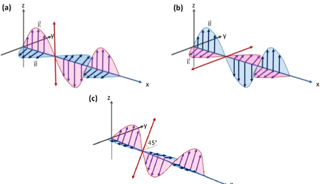
The plane wave is an optic transverse wave composed of electric and magnetic field that could oscillate randomly, but always perpendicular to each other and to the propagation path. This non-coherence characterizes the sun light, which is called non-polarized. Using special optical components, we can intervene on the natural light and fix the direction of its electric field rendering it polarized. The polarization of light often refers to the property of its electric field, which oscillates in only one direction: vertically, horizontally or even diagonally (Figure 1.17). All these three orientations can be attributed as linear polarization, which is the most commonly used.
Figure 1.17: Linear vertical (a), horizontal (b) and diagonal (c) polarization. The red arrow illustrates the direction of polarization and the x-axis the direction of propagation.
However, in addition to linear polarization there are also other types such as circular and elliptical.
Clockwise Polarization Counter- Clockwise Polarization
(a) (b)
Figure 1.18: Clockwise or right hand (a) and counter-clockwise or left hand (b) circular polarization observed from the source [92].
The elliptical polarization differs from the circular polarization in amplitude or in phase. The elliptical polarization consists of two perpendicular components with 90° phase difference but with unequal amplitudes or even with equal amplitudes but phase φ ≠ ±π/2+ mπ. This inequality makes the eccentricity less than 1 (e=1 for the circle) that attributes the form of ellipse to the extreme points of the electric field. There are also two orientations of the right and left hand for the propagation of the waves (Figure 1.19).
Despite the fact that the elliptical polarization can be considered as a special case, it is in reality the dominant category that includes the two previous polarizations, linear and circular.
(a) (b)
In our brief analysis, the polarization is described by the superposition of all the extreme points of electric field along time and space. However, if we examine the polarization at a given moment making a spatial cross-section of the beam we can distinguish additional categories [94]. Three types are typically mentioned, radial, azimuthal and spiral polarization (Figure 1.20) that are obtained with special optical vortex converters [95,96].
Figure 1.20: Local change of direction of polarization with red arrows on cylindrical vector beams [96].
As it will be discussed below, the polarization of light is a state that interacts with matter such as other properties like orientation and intensity. Fresnel Equations and Snell-Descartes law give a total overview of these interactions when light passes from one optical medium to another. Next, we will examine the light behavior when it impinges on corrugated surfaces such as diffraction gratings.
Diffraction grating dependence on light polarization
To form complex polarization states [97–99] or even use them to excite light in non-standard grating geometries (see Chapter 3) special diffraction elements are extremely useful. In other words, the relation between polarization and diffractive optical element is inextricably linked and will be discussed below.
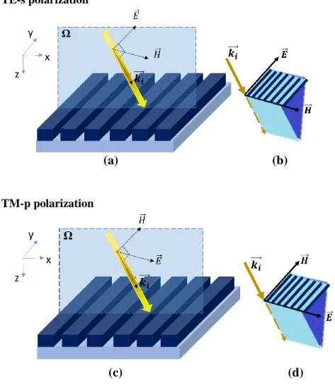
Initially, we consider the interaction of electromagnetic light with a simple rectangular diffraction grating on a substrate. When light impinges on a grating with collinear incidence, the field vectors form a trihedral with the wave vector that lies in the plane of incidence Ω (Ω defined by 𝑘⃗⃗⃗ and z direction). Transverse electric or transverse magnetic polarization is 𝑖
p-polarization, the vector of the magnetic field is normal to the plane of incidence or parallel to the lines of the grating and the electric field vector is in the plane of the incident wave. These configurations are illustrated in Figure 1.21.
TE-s polarization
(a) (b)
TM-p polarization
(c) (d)
Figure 1.21: Polarization of incident light in relation to grating lines. TE (a) and TM polarization (c) of the incident k⃗⃗⃗ light and representation of the vectors forming a trihedral (b), (d) respectively. i
1.5 Waveguide Resonant Grating
Structure of a Waveguide Resonant Grating (WRG)
The Waveguide Resonant Grating (WRG), also referred as Subwavelength Resonant Grating (SWG) or Guided Mode Resonant Grating (GMR) is a configuration usually consisting of a substrate, a high-index thin waveguide film in optical contact with an additional transparent layer in which a grating is etched.
Prior to the presentation of the resonance mechanism (Section 1.6), the planar waveguide under the diffraction grating and the propagation of the modes within the guide are studied in the following Section 1.5.2.
Figure 1.22: Geometrical structure of 1D Waveguide Resonant Grating.
Where:
ni, ng, nwg, ns are the refractive indices of superstrate, grating, waveguide and substrate
respectively.
𝑘𝑖
⃗⃗⃗ and 𝜃𝑖 are the wave vector and angle of the incident beam respectively.
𝑘𝑟
⃗⃗⃗⃗ and 𝜃𝑟 are the wave vector and angle of the reflected wave in the m=0 diffraction order.
d, w are grating height and waveguide thickness.
f, s are grating ridge and grating groove width respectively.
𝐹𝐹 =𝑓𝛬 , the Filing Factor or Duty Cycle: (For binary gratings, the FF corresponds to Duty cycle).
𝐴𝑅 =𝑑
Planar Waveguide
Dispersion EquationIn this Section, we decompose the waveguide resonant problem by initially focusing on the study of the planar waveguide-slab. As described above the insertion of light in a planar waveguide is realized by a grating or alternatively by a prism. After light insertion and mode propagation in the waveguide, a sharp resonance appears if only two specific conditions are fulfilled:
- the total reflection 𝑛𝑠< 𝑛𝑒𝑓𝑓< 𝑛𝑤𝑔 , with neff the effective index, which states a number that relates the velocity of a light beam in the waveguide, seen as a propagative mode in the waveguide (for a given polarization and considering ns > ni).
- the constructive interference in the planar waveguide, which follows the dispersion equation.
The figure below illustrates the optical path of light and the needed geometry for the second condition (Figure 1.23).
Figure 1.23: Representation of light propagation in a planar waveguide.
The plane wave in the medium of the waveguide is described by 𝑒𝑗(𝜔𝑡−𝑘⃗ 𝑤𝑔𝑟 ), where
|𝑘⃗ 𝑤𝑔|=𝑘0 𝑛𝑤𝑔= 2𝜋
𝜆0𝑛𝑤𝑔 expresses the wave vector k0 that is the free space wave vector and nwg
the refractive index of the waveguide. The propagation of the wave in the layer of the waveguide will take place if the wave interferes with itself constructively, i.e. if the phase difference between the two wave fronts is the same along their optical paths AB and CD and equal to 0 or 2mπ.
The phase shifts φ(wg-i) and φ(wg-s) are due to the total reflection at each interface i (cover (i) or
substrate (s)).
Following the geometry of the figure, we take:
CD = w
sin 𝛼𝑚 and AB = CB 𝑐𝑜𝑠𝛼𝑚
Therefore, the related phases become:
ΦAB= kwg
w (cos2𝛼𝑚−sin2𝛼𝑚)
sin 𝛼𝑚 and ΦCD = kwg w sin 𝛼𝑚
The phase differences at the interfaces are equal to:
𝜑𝑤𝑔−𝑗 = −2 arctan √cos2𝛼 𝑚−( 𝑛𝑗 𝑛𝑤𝑔 ⁄ )2 𝑠𝑖𝑛𝛼𝑚 (for TE polarization) 𝜑𝑤𝑔−𝑗 = −2 arctan ( 𝑛𝑤𝑔 𝑛𝑗) 2 √cos2𝛼𝑚−( 𝑛𝑗 𝑛𝑤𝑔 ⁄ )2 𝑠𝑖𝑛𝛼𝑚 (for TM polarization)
With 𝑛𝑗= 𝑛𝑖, 𝑛𝑠 the refractive indices for cover and substrate respectively.
We define the effective index as neff = nwg cos𝛼𝑚 and the constant propagation β of the guided
wave in the waveguide medium that is inseperably connected to the effective index by β = kwg cos𝛼𝑚= k0 neff.
The replacements of the above relations to the initial Equation 1.4 give:
ΔΦ (CD-AB) = 2mπ = 2𝑘0𝑤√𝑛𝑤𝑔2− 𝑛𝑒𝑓𝑓2 − 2arctan 𝜉𝑤𝑔,𝑠√ 𝑛𝑒𝑓𝑓2 −𝑛𝑠2 𝑛𝑤𝑔2 −𝑛 𝑒𝑓𝑓2 − 2arctan 𝜉𝑤𝑔,𝑖√ 𝑛𝑒𝑓𝑓2 −𝑛𝑖2 𝑛𝑤𝑔2 −𝑛 𝑒𝑓𝑓2 Equation 1.5 With m = 0, +1, +2… and 𝜉𝑤𝑔,𝑗= 𝑛𝑤𝑔2 𝑛𝑗2
⁄ for TM polarization and 𝜉𝑤𝑔,𝑗 = 1 for TE.
The above Equation 1.5 is known as dispersion equation and calculates the effective index of the waveguide according to the polarization TE or TM. The relation implies that every m order
Mode Cut-off
The thickness of the waveguide will determine the number of modes that will be propagated within it. Multimode or single mode behavior can be forecasted a priori through the frequency for which the propagation angle 𝛼𝑚 reaches its critical value 𝛼𝑐𝑟 or in other words when neff = ns.
For TE polarization the cut off frequency ωc and thus the cut-off wavelength λc is given by:
𝜔 𝑐|cut off = k0= 2𝜋/𝜆𝑐 = 1 𝑤√𝑛𝑤𝑔2 −𝑛 𝑠 2[𝑚𝜋 + arctan√ 𝑛𝑠2−𝑛 𝑖 2 𝑛𝑤𝑔2 −𝑛𝑠2] Equation 1.6
And for TM polarization:
𝜔 𝑐|cut off = k0= 2𝜋 𝜆𝑐 = 1 𝑤√𝑛𝑤𝑔2 −𝑛𝑠2 [𝑚𝜋 + arctan ( 𝑛𝑛𝑤𝑔2 𝑠 2 √ 𝑛𝑠2−𝑛𝑖2 𝑛𝑤𝑔2 −𝑛 𝑠2 )] Equation 1.7 With m = 0, +1, +2...
In the case of a multimode waveguide, the dispersion equation ( Equation 1.5) can be simplified considering that the “arctan” terms are small compared to 𝑘0𝑤√𝑛𝑤𝑔2 − 𝑛𝑒𝑓𝑓2 . Then,
neff varies with the square of its order: 𝑛𝑒𝑓𝑓 ≅ 𝑛𝑤𝑔− 1 2𝑛𝑤𝑔(
𝑚𝜋 𝑘0𝑤)
2
As mentioned before, the propagation constant β is dependent on the frequency 𝛽 =𝜔
𝑐𝑛𝑒𝑓𝑓= 𝑘0𝑛𝑒𝑓𝑓 = ( 2𝜋
𝜆0) 𝑛𝑒𝑓𝑓. If we solve the dispersion equation numerically for different
guided modes, we can plot the dispersion diagram that gives explicitly the region of the guided modes (Figure 1.24). This region is placed between two straight lines 𝛽 =𝜔
𝑐𝑛𝑠 and 𝛽 = 𝜔
𝑐𝑛𝑤𝑔
and describes the propagation of the plane waves in the homogeneous infinite media of index 𝑛𝑠 and 𝑛𝑤𝑔.
Propagated power of the modes
Every mode carries an energy, therefore a power along its optical path. This power can be expressed through the Poynting theorem according to:
𝑃 = ∫ 𝑆 𝑑𝑟⃗⃗⃗⃗ Equation 1.8 with 𝑆⃗⃗ =1 2𝑅𝑒(𝐸⃗ × 𝐻⃗⃗ ∗) and 𝑑𝑟⃗⃗⃗⃗ = 𝑎 𝑧 ⃗⃗⃗⃗ 𝑎⃗⃗⃗⃗ 𝑑𝑦𝑥 .
For a TE mode inside the waveguide parallel to the x-axis (perpendicular to the grating lines), the vertical transverse component y of magnetic field is 𝐻𝑦=
𝛽
𝜔𝜇0𝐸𝑥, and after the replacement
in (Equation 1.8), the carrying power of a mode is:
𝑃 = 𝛽 2𝜔𝜇0 ∫ |𝐸𝑥|2 ∞ −∞ 𝑑𝑦 Equation 1.9
For TM polarization, the relation becomes:
𝑃 = 𝛽 2𝜔𝑛𝑤𝑔2 𝜀0 ∫ |𝐻𝑥|2 ∞ −∞ 𝑑𝑦 Equation 1.10 with 𝐸𝑦= 𝛽 𝜔𝑛𝑤𝑔2 𝜀0𝐻𝑥
In the waveguide region, the power is related to the wave vectors in each medium (cover, substrate, waveguide) and results as follows:
𝑃 = 𝛽 4𝜔µ0 𝐵12𝑘𝑖 2+ 𝑘 𝑤𝑔2 𝑘𝑤𝑔2 [ 1 𝑘0𝑘𝑠 + 1 𝑘0𝑘𝑖 + 𝑤] Equation 1.11
With B1 a constant expressing the field amplitude in the interface cover-guide and
𝑘𝑠= √𝑛𝑒𝑓𝑓2− 𝑛𝑠2, 𝑘𝑤𝑔= √𝑛𝑤𝑔2− 𝑛𝑒𝑓𝑓2 and 𝑘𝑖 = √𝑛𝑒𝑓𝑓2− 𝑛𝑖2
The parenthesis can be seen as the effective width or the electromagnetic width of the waveguide and is expressed like:
𝑤𝑒𝑓𝑓= 1 𝑘0√𝑛𝑒𝑓𝑓2 − 𝑛𝑠2 + 1 𝑘0√𝑛𝑒𝑓𝑓2 − 𝑛𝑖2 + 𝑤 Equation 1.12
1.6 Resonance Study
Resonance Principle
When an incident beam impinges in a WRG structure (Figure 1.22), part of the beam is directly transmitted and part is diffracted and trapped in the waveguide layer as waveguide modes. During propagation, the guided light leaks out of the waveguide and interferes destructively with the transmitted beam while constructively with the reflected in the superstrate. This leads to complete interference of light yielding to zero transmission [18], [101] (Figure 1.25). Depending on the specific wavelength and angular orientation of the incident light, a very high reflection occurs, the so-called resonance. In normal incidence and for a monomode waveguide, the structure resonates with only one wavelength whereas in oblique incidence two resonating wavelengths appear (Figure 1.26). The oblique incidence causes the splitting of the resonance (Figure 1.27) followed by coupling of the +1 and −1 diffracted orders to the leaky modes of the waveguide appearing at two different wavelengths [102]. For a large range of angles the symmetrical gap starting from 0°, increases with the angle increment.
These resonances display a Fano or Lorentzian profile with linewidth as narrow as 0.1 nm [103]. The reflection coefficient or resonance is the contribution of the eigenmodes of the grating presented as perturbed area with strong scattering by ridges and grooves. The resonance can only be achieved by taking into account an infinite waveguide grating excited by means of a plane wave.
Thanks to the sharp resonance of WRG, filtering applications are highly recommended. In addition, the use of transparent dielectric-based configurations avoid thermal effects in contrast to metallic structures [104].
(a) (b)
Figure 1.25: Schematic representation of the resonance process through the mode coupling by a corrugated grating with normal incidence (a) and oblique incidence (b). The letter s marks the radiated
beam outward the cladding.
Figure 1.26: Efficient resonances in Reflectance and Transmittance as a function of wavelength λ for a monomode waveguide under normal (a), (c) and oblique incidence θi = 15° (b), (d).
Figure 1.27: Spectral distribution of a wide range of oblique angles.
Mode Coupling
The mode coupling description imperatively demands a geometrical representation to include all the simultaneous actions taking place in the structure; i.e. the impinging incident light (normal or oblique) to the grating, the mode excitation by the resonant wavelength and the propagating direction of the orders. All the three parameters can be designed in the Ewald sphere and simply calculated by the grating equation that fulfills the coupling synchronism and incorporates the effective index 𝑛𝑒𝑓𝑓 of the waveguide:
𝑘0𝑛𝑖sin 𝜃𝑖 + 𝑚𝐾𝑔 = 𝑘0𝑛𝑒𝑓𝑓 Equation 1.13 From which results:
𝑛𝑒𝑓𝑓= m𝜆0
𝛬 +𝑛𝑖sin 𝜃𝑖 Equation 1.14
The replacement of the orders 𝑚 in the formula sets the value of 𝑛𝑒𝑓𝑓, which in turn has to fulfill the total reflexion criterion 𝑛𝑠 < 𝑛𝑒𝑓𝑓 < 𝑛𝑤𝑔.
The mechanism of the Ewald Sphere will be below explained notably based on the most commonly encountered structure in this thesis (binary diffraction grating of positive photoresist (PR) on a TiO2 solgel waveguide and a glass substrate) (Figure 1.28). The technique can be
Figure 1.28: Binary structure of photoresist, TiO2 solgel and glass substrate with ng = 1.67 and k = 0,
nwg = 2.34 and ns = 1.511 respectively.
The study of the Ewald Sphere is analyzed extensively for two types of incidence; normal and oblique under TE polarization.
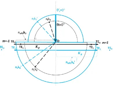
Normal Incidence
Considering a normal incidence and a monomode waveguide resonant grating, a coupling between the incident light beam and the fundamental mode occurs. The vertical line in the Ewald circle represents the incident beam and guarantees the existence of symmetry; two propagative (forward) and contra- propagative (backward) orders 𝑚 = ±1 excite the mode that lies at equal distance from the origin of axis O, represented by the distance corresponding to the vector norm of the propagative mode equal to 𝑘0𝑛𝑒𝑓𝑓 and equal to the vector 𝐾𝑔 in the case
of normal incidence, when synchronism phase and mode excitation occur. It should be noted that the mode is placed outside the substrate and in the proximity of the substrate semicircle (Figure 1.29). This is completely legitimate since the effective index of the mode is usually slight larger than the refractive index of the substrate. In the opposite case, no coupling would appear between incident beam and waveguide propagative mode. Finally, the coupling leads to a high resonance and the type of mode is depicted with the form of lobes in a 2D electric field (Figure 1.30) scan by Modal Collinear Programming (Section 1.7). Using the convention of axis orientation depicted in (Figure 1.12) for TE polarization. The lobes represent the propagation of standing waves in a single or more periods of the structure.
Figure 1.29: Ewald sphere representation for a monomode waveguide of effective index under normal incidence illumination for TE polarization.
(a) (b)
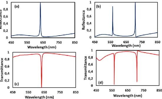
Figure 1.30: Resonance for TE polarization at λ = 636 nm (a) and TE0 mode electric field amplitude
distribution Ey scanned for a single period at the same resonant wavelength (b). The tested structure consists of d = 100 nm of photoresist grating, w = 102 nm of waveguide width, 340 nm of period and
DC = 0.5.
For bimodal guide and normal incidence, two modes are excited. Having already calculated the appropriate width of the waveguide for two mode-propagation in the TE polarization, we demonstrate that two distinct wavelengths yield to the excitation of the fundamental TE0 and
(a) (b)
Figure 1.31: The left resonant wavelength peak corresponds to λ′ = 586.5 nm and the right to λ = 726.75 nm exciting the TE1 and TE0 mode respectively (a), 2D electric field amplitude
distributions on λ′ and λ respectively scanned for a single period (b). The tested structure consists of a TiO2 waveguide of w = 250 nm and a subwavelength binary resist grating
of d = 100 nm, Λ = 340 nm and DC = 0.5.
Following the geometry of the configuration, each wavelength corresponds to separate Ewald circle with different circle radius for superstrate and substrate medium. The highest wavelength (λ = 726.75 nm) corresponds to the smaller Ewald circle and excites the fundamental mode TE0.
The 𝑛𝑒𝑓𝑓0 of the TE0 is calculated by the (Equation 1.14) and is equal to 2.13, therefore placed
outside the semicircle of its substrate. The smaller wavelength (λ′ = 586.5 nm) with bigger Ewald circle excites the TE1 of 𝑛𝑒𝑓𝑓1 = 1.725 and thus is placed in proximity to the substrate.
In this Ewald circle the fundamental mode is placed at the left of TE1 (𝑛𝑒𝑓𝑓1< 𝑛𝑒𝑓𝑓0) and
cannot be reached with the same Kg vector. As a fixed value imposed by the structural
proceeding, the Kg = 2π/Λ unit is the same for both wavelengths λ and λ′ and equal to 𝑘0𝑛𝑒𝑓𝑓0
Figure 1.32: Ewald sphere configuration for bimodal waveguide under normal incidence illumination for TE polarization for two wavelengths λ (black) and λ′ (blue).
For high multi-modal waveguide and normal incidence, the mechanism remains the same but becomes more and more cumbersome to represent. For TM polarization, the approach is identical but prior calculations need to be included for the waveguide width.
Oblique Incidence
In oblique incidence, the incident wave vector is tilted according to the incidence plane normal to the grating grooves, with an angle corresponding to the incident angle i.
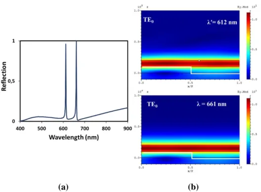
For a monomode waveguide and a tilted angle, the resonant reflection peak splits into two peaks with different amplitudes. Now, the 2D electrical field distribution for the mode identification appears as a homogeneous zone in the guide (Figure 1.33).
(a) (b)
Figure 1.33: The 612 nm resonance peak excites the TE0 mode (forward) and the 661 nm the TE0
mode (backward) (a). 2D electric amplitude field distribution for both excitation wavelengths (b). The current structure consists of a TiO2 waveguide of w = 102 nm and the incidence angle of study is 5°.
The other parameters are as previously (d = 100 nm, FF = 0.5, Λ = 340 nm).
Now, the 2D electric field distribution cannot clearly distinguish the TE mode propagation direction. Further 2D scanning of power flow is helpful for the order identification.
(a) (b)
Figure 1.34: 2D power flow scanning along x direction. The 612 nm resonance peak excites the TE0
is designed from the end of the incident’s beam projection and with a fixed period, 𝐾𝑔 can excite a mode through the positive or negative m = ±1 order. As seen schematically in the forward propagation direction, the distance of the mode is equal to 𝑘0′𝑛𝑒𝑓𝑓0= 𝑛𝑖𝑘0sin 𝜃𝑖 + 𝐾𝑔 while 𝑘0𝑛𝑒𝑓𝑓0 in the backward propagation. The TE0 mode is not placed symmetrically since the
𝑘0𝑛𝑒𝑓𝑓0 differentiates from each semicircle (Figure 1.35).
Figure 1.35: Ewald sphere for oblique incidence at 5° for a monomode waveguide for TE polarization for two wavelengths.
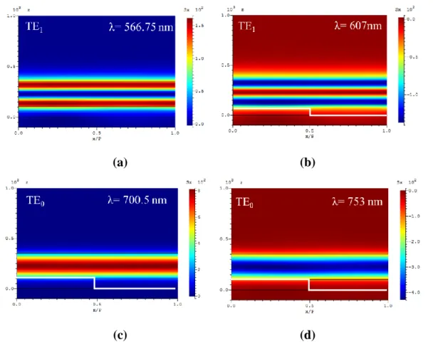
With a different configuration, it might be also possible to excite a mode other than the fundamental one, with a more elevated order, m = ±2 for instance (Figure 1.36). In such a case, two resonant wavelengths appear having different amplitudes but neither of them is at 100% since part of the energy is also carried by the modes excited by the ±1 orders.
For a waveguide supporting n modes and an oblique incidence, it is clear that the resonance peaks become 2n as well as the number of the Ewald configurations. Equivalently, the direction of propagation is calculated for each wavelength through the coupling synchronism and the mode identification is realized through the 2D electric field distribution and power flow (Figure 1.37).
(a) (b)
Figure 1.36: Bimodal waveguide with excitation mode resonances that correspond to λTE1=566.75 nm,
λTE1=607 nm, λTE0=700.5 nm and λTE0=753 nm (a) with the corresponding fields amplitude starting
from top left (b). The structure consists of d = 102 nm PR, w = 250 nm waveguide, Λ= 340 nm period, DC = 0.5 and θi = 5°.
(a) (b)
(c) (d)
Polarization dependence of the resonance response
In both cases TE or TM, the polarization can influence the resonance by shifting the position of the wavelength or even by broadening the linewidths of the peaks (Figure 1.38).
The primary reason for this is due to the effective index difference for TE and TM propagative modes in the waveguide.
Moreover, the resonance peak linewidth difference can be attributed to the radiation coefficient that is large for TE polarization, while very small for TM. The TE polarization has a short propagation length in the waveguide, therefore a high radiation coefficient (Lp=1/) (See also Section 1.6.4) that results in a wide spectral width. With another perspective, we could consider the material particles of the grating corrugation as small dipoles that can be excited differently by each polarization when illuminated under normal incidence. For TM polarization, the vibration of the electric field in the grating corrugation is normal to the waveguide plane. This vibration movement provokes a parallel to the grating lines radiation inducing simultaneously a damping radiation at the z-axis of our interest. In contrast, for TE polarization the vibration of the electric field is essentially parallel to the grating lines yielding a reinforced radiation at z-axis [105].
Figure 1.38: Position shift and spectral width difference between TE and TM polarization under normal incidence for a structure with d = 376 nm, w = 340 nm, Λ = 960 nm, s = 480 nm, ns = 1.45,
Dimensioning resonance with optogeometrical grating waveguide
parameters
To meet the filtering purposes of WRG structures, narrow spectral and angular bandwidths are required. Structural features strongly influence the resonance characteristics, so it is necessary to handle them properly for resonance shaping and tuning. The characteristics of waveguide grating coupling depend on a large number of optogeometrical parameters (wavelength, period, incidence angle, waveguide index and thickness, grating depth, duty cycle…).
Shin et al. demonstrated dependence of the linewidth (Δλ/λ) on the modulation of a grating Δε = nH2-nL2 and the duty cycle in both TE and TM polarizations in a single layer configuration
(Figure 1.39) [106]. It is shown, that maximum linewidth is achieved with DC = 0.5.
Figure 1.39: Filter linewidth dependence on the modulation index (a) and filling factor (b) for a single layer reflection grating [106].
Moreover, he pointed out that the profile of the grating can have an impact on the resonance. The rectangular grating presents wider resonance, which is excited at a shorter wavelength compared to that of the narrow trapezoidal (Figure 1.40).

![Figure 1.40: Grating form dependence on the resonance for a triple-layer WRG structure under TE polarization [106]](https://thumb-eu.123doks.com/thumbv2/123doknet/14561064.726405/60.892.282.612.100.387/figure-grating-dependence-resonance-triple-layer-structure-polarization.webp)
![Figure 1.41: Decomposition of a blazed grating in different layers leading to the staircase effect [113]](https://thumb-eu.123doks.com/thumbv2/123doknet/14561064.726405/63.892.172.755.109.419/figure-decomposition-blazed-grating-different-layers-leading-staircase.webp)
![Figure 2.1: Representation of integrated circuits on a semiconductor wafer [18] (a), lotus plant characterized by hydrophobicity and SEM images (A-D) for the corresponding replicated biomimetic](https://thumb-eu.123doks.com/thumbv2/123doknet/14561064.726405/74.892.244.655.403.667/representation-integrated-semiconductor-characterized-hydrophobicity-corresponding-replicated-biomimetic.webp)